

Abstract
This article reports the thermal conduction properties of Si/a-SiO2 heterostructure with two different interfaces: weak and strong coupling strength through molecular dynamics simulation. The size and temperature dependencies on the interfacial thermal resistance of the weak coupling interface are larger than those of the strong coupling interface. The thermal conduction in Si/a-SiO2 shows strong anisotropy. The thermal conductivity, interfacial thermal resistance, and enhancement of the anisotropy can be modulated by changing the strains applied to the heterostructures. This work provides an optional way to design the silicon-based heterostructures considering heat insulation and heat dissipation.
Export citation and abstract BibTeX RIS
1. Introduction
As the size of the devices continues to decrease, the interfacial heat transfer between different materials has a more important impact on the overall heat transfer performance. To achieve good thermal management, a solid-solid interface can dissipate the heat generated in the equipment [1]. Due to the interface and the different properties of the materials on both sides of the interface, it will form a thermal resistance in heat transfer [2]. The most common heterostructure in Micro-Electro-Mechanical-Systems (MEMS) is silicon on insulator (SOI). Many micro-devices are based on the SOI wafer. The a-SiO2 layer is a typical amorphous oxide layer. There is an interface between the a-SiO2 thin films and the bulk monocrystalline silicon in the SOI wafers [3]. The extremely low thermal conductivity of a-SiO2 will greatly affect the heat transfer of the devices [4]. Due to the unclear understanding of the interfacial thermal performance of SOI wafers, it is difficult to conduct thermal management of nano-devices.
Experiments and simulations are commonly used to study the thermal properties of the Si/SiO2 structure. The common simulation methods to understand the thermal conduction across the solid-solid interface are the acoustic mismatch model (AMM) and the diffuse mismatch model (DMM) [5]. Due to the shortcomings in these two methods, the molecular dynamics (MD) simulations are increasingly used at the atomic-level [2, 6–8]. Liang et al [9]. studied phonon transmission in Si/a-SiO2/Si. The results showed that structural disorder is the main reason inducing phonon attenuation. Chen et al [10]. found the interface coupling has a great influence on the Kapitza resistance between the amorphous silicon dioxide and crystalline silicon. Deng et al [11]. studied the anharmonic phonon scattering at the interface in a Si/SiO2/Si heterostructure. Lampin et al [12]. introduced a new method called 'approach-to-equilibrium' MD (AEMD) to extract thermal boundary resistance in Si/a-SiO2. Li et al [13]. found the defect between the SiO2 substrate and the h-BN mainly affects the heat conduction at the interface using the differential 3 ω method. Hurley et al [14]. measured the Kapitza resistance across the Si/SiO2 which is around 2.3 × 10⁻⁹ m2 K W−1. Other crystal/amorphous heterostructures have also attracted the author's attention. France-Lanord et al [15, 16]. constructed amorphous/crystalline silicon superlattices and nanowires. Our previous work [17] also discussed the size, temperature, and strain effect on the thermal conduction in amorphous/crystalline silicon superlattices. Bazrafshan et al [18]. studied the thermal conductivity of pristine/amorphous graphene.
Most of the previous works focused on the interface characteristics, Kapitza thermal resistance, and phonon conduction characteristics. Some studies were concerned with how to modulate the thermal conduction properties of the material to meet engineering requirements [19] Strain is an optional way to change the thermal conductivity of such materials without changing their composition [20–22]. Researchers have discussed the coupling properties of thermal conduction and strain. Bhowmick et al [23]. studied the effect of strain on the thermal conductivity of an insulating solid. The results showed that the thermal conductivity is related to temperature and strain. Li et al [24] proposed that the application of stress/strain on materials provides a mechanism to adjust the thermal conductivity of materials dynamically. Similar studies have revealed the dependence of thermal conductivity on the applied strain [4, 25–27]. According to different kinds of materials [28], the strain effect remains controversial. The effects of strain on superlattice and heterostructure were also reported [17, 29–31]. The internal strain in literature [31] was caused by interface mismatch during material preparation. Others were caused by external artificial strain to simulate the actual engineering situation. As we know, the strain may also affect the thermal conduction of the materials on both sides of the interface and the whole system. The comprehensive effects of the strain are worth studying. In the engineering applications, besides the interfacial thermal conduction, the heat conduction parameters of whole material are also needed.
In fact, up to now, there is no specific work about the effect of strain on the thermal properties of the Si/a-SiO2 heterostructures. It motivates us to study the effect of strain on the thermal properties of the Si/a-SiO2 heterostructures using MD simulations in this paper. This work and the results are helpful to accurately design the silicon-based nano-devices when considering heat insulation and heat dissipation.
2. Methodology
2.1. The simulation method
Large-scale Atomic/Molecular Massively Parallel Simulator (LAMMPS) MD package [32] is a classical MD code with a focus on materials modeling used in all our simulations. The Nonequilibrium molecular dynamics (NEMD) method can be realized through many variations, including different boundary conditions and different ways of generating the temperature gradient. According to the recent research [33] about the selection of calculation parameters on the NEMD method. The Langevin thermostat is the optimal method to control the temperature of the heat source and heat sink.
By the Langevin method, we can even calculate the temperature gradient directly from the temperature difference between the heat source and heat sink, instead of fitting the temperature distribution curve as before. However, for the extraction of interfacial thermal resistance, we still need to fit the temperature curve to obtain the temperature difference in the interface. The basic Langevin method for calculating the thermal conductivity is illustrated in figure 1(a). We set a fixed boundary layer at both ends of the material. Next to the boundary layer are the heat source and heat sink (HOT layer and COLD layer in figure 1). Then we can set the desired temperature in the heat source and heat sink. After forming a stable temperature distribution in the system, the thermal conductivity is based on the Fourier equation:
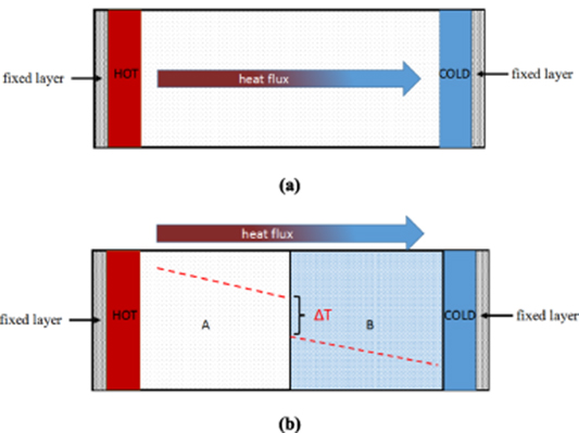
Figure 1. The Langevin NEMD.
Download figure:
Standard image High-resolution imageWhere J represents heat flux, dT/dx represents the temperature gradient. For the interfacial thermal resistance, the equation is:
Where J represents heat flux, ΔT represents the temperature drop in the interface shown in figures 1(b), A and (B) represent two different materials, the red dotted line represents the temperature distribution.
We should minimize energy and relax the structure at the beginning of the simulation. Then, we put the model into the isothermal-isobaric (NPT) ensemble with the desired temperature and pressure over 4 ns. After that, the Langevin method was performed along with a micro-canonical ensemble (NVE) over 4 ns. Then, according to equation (1) and equation (2), we can get relevant results.
2.2. The model of Si/a-SiO2
The generation of our model consists of two main steps: the formation of amorphous silica and the structure of Si/a-SiO2. The process will be described in detail below.
2.2.1. The amorphous silica.
Amorphous silicon dioxide is formed by high-temperature melting and annealing of the crystalline silicon dioxide. Two kinds of crystal materials are commonly used in the literatures: α-quartz and β-cristobalite [11, 12, 34]. As the final non-crystal, there should be no difference in the choices of origin crystal. The β-cristobalite is chosen in our work. For all of our models, first, we build the β-cristobalite structure. The initial lattice parameter: a = b = 4.9717 Å, c = 6.9223 Å [35]. Then we perform energy minimization on the model at room temperature. The model is then heated to melting state (T > 6000 K) for about 2 ns. Then keep the melting state for another 1 ns. Finally, the annealing process must be very slow to prevent re-crystallization of the disordered structure. Therefore, we should choose a very low annealing speed. In this simulation, the cooling rate is about 1 K ps−1. The Radial Distribution Functions (RDFs) are shown in figure 2. The structural parameters of the a-SiO2 are compared with the literatures in table 1. In order to verify the reliability of our material structure, we calculate the heat current autocorrelation function (HCACF) and we get convergent results of thermal conductivity by using BKS potential in equilibrium molecular dynamics (EMD). The results are 2.04 ± 0.03 (W/mK) as shown in figure 3. They are in agreement with the literature [4].

Figure 2. The RDFs of a-SiO2.
Download figure:
Standard image High-resolution image
Figure 3. The calculation results of EMD (a) Thermal conductivity. (b) Heat current autocorrelation function.
Download figure:
Standard image High-resolution imageTable 1. Parameters of amorphous silica.
| parameter | This work | Literatures [36, 37] |
|---|---|---|
| Density(g cm−3) | 2.26 | 2.28(simulation), 2.20(experiment) |
| Si-Si(Å) | 1.65 | 1.65(simulation),1.608(experiment) |
| O-O(Å) | 2.625 | 2.7 ± 0.2(simulation),2.626(experiment) |
| Si-Si(Å) | 3.175 | 3 ± 0.2(simulation),3.077(experiment) |
In the whole process, the choice of interatomic forces is Tersoff potential. Tersoff potential is a very suitable function for studying the thermal and mechanical properties of Si. In a-SiO2, Tersoff potential is also commonly used in previous literatures [9–12]. Compared with BKS potential, the Tersoff potential has a smaller difference compared to experimental value [4, 38] and higher computing efficiency.
2.3. Building the Si/a-SiO2
Figure 4 shows the complete process of material preparation. There is no direct periodic replication after each step of model generation to get a larger model. Because this will introduce artificial periodicity into the larger structure. Although it can eliminate the problem of artificial periodicity by heating, melting, and annealing the structure.

Figure 4. Modeling process.
Download figure:
Standard image High-resolution imageIn the preparation of a-SiO2, we fix the size of the cross-section and only control the pressure of the material perpendicular to the interface in the NPT ensemble (For more details, please refer to the supplementary file). Thus, Si and a-SiO2 will have the same cross-sectional area. In addition, in the combining process, we only fix the length perpendicular to the interface and control the pressure in the other two directions in the NPT ensemble. In the actual Si/a-SiO2 structure, the interface is not pure Si or a-SiO2 as shown in figure 5. We can observe the existence of the transition regions (red box).

Figure 5. Structure of the Si/a-SiO2.
Download figure:
Standard image High-resolution imageAfter simplification, the practical methods combine the crystalline silicon and amorphous silicon with different combination distances [10]. As shown in figure 4(e), we put two materials together. The placement distance will affect the bonding strengths of the interface. According to the spacing selection principle defined in reference [10], there are basically two types of interface combinations: strong combination and weak combination. They represent strong and weak bonding strength in the interface. Generally speaking, the initial distance between the two materials should not exceed 3 Å, which is usually related to the interaction potential. Here we consider two situations according to reference [10], the initial distance 0.3 Å is the strong combination and initial distance 2.7 Å is the weak combination. They are described in figure 6.

Figure 6. Structure of the Si/a-SiO2.(a) Strong combination (b) Weak combination.
Download figure:
Standard image High-resolution imageWhen we combine these two materials. First, energy minimization and structure relaxation are performed. After relaxation, the temperature of the system is slowly increased to 1000 K over 500 ps. The 1000 K is insufficient to melt silicon or amorphous silica [39], but high enough for atomic rearrangements in the Si-SiO2 interface region. The system is kept at 1000 K for 500 ps and then cooled to 300 K at a cooling rate of 1 K ps−1.
The interfacial heat transfer mechanism can also be further studied by the overlap factor of the material vibration spectrum, which can be better to understand the effect of interfacial interaction on thermal conductivity [40]. The phonon density of states (PDOS) can be calculated by the Fourier transform of velocity autocorrelation function:
Where D1 (ω) and D2 (ω) denote the PDOS of Si and a-SiO2 atoms at the interface at frequency ω. Overlap factor S denotes a matching degree in phonon spectrums [29].
3. Results and discussion
3.1. The interface thermal resistance and thermal conductivity of Si/SiO2
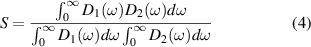
The size effect is considered in NEMD calculation. Generally, the two main factors that usually affect the thermal properties of a heterostructure material are interface size and length of the material. According to the previous literatures, it is not necessary to choose a large cross-section to ensure that the corresponding boundary effect can be eliminated. Therefore, the cross-sectional area of 4 a × 4 a (a represents the lattice constant of crystal silicon, a = 5.42 Å) is chosen in this paper. However, good consistency of cross-plane conductivity values obtained by both MD and NEMD was found [15]. This may be due to the extremely low thermal conductivity of the amorphous layer. The literature [41] shows that thermal conductivities of amorphous silicon dioxide and crystalline silicon dioxide, increase with the increase of thickness. However, amorphous silicon dioxide converges at a very low thickness (about 4 nm), which is much smaller than the mean free path (MFP) of crystalline silicon dioxide [42]. Therefore, with the size change, the main contribution of thermal conductivity may be provided by monocrystalline silicon. Figure 7 shows the temperature curve of the Si/a-SiO2 at room temperature. The ΔT is the temperature drop in the interface obtained by fitting the temperature curves.
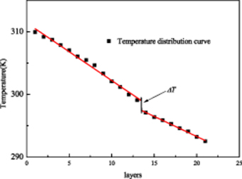
Figure 7. The temperature curve of the Si/a-SiO2 and the interfacial temperature difference ΔT.
Download figure:
Standard image High-resolution imageIn current applications, the thickness of the silicon film typically ranges from approximately 5 nm to 1.5 μm. The thickness of silica is usually from 10 nm to 5 μm [43, 44]. The SOI wafers can be adapted to most device structures, from ultra-thin CMOS to thick-film power transistors and sensors. Thus the proportion and thickness of these two materials are very different for different applications. Because it is difficult to simulate large-scale materials in MD simulations, different proportions of materials are selected in the study in the finite length calculation. In order to qualitatively analyze the influence of the proportions on the thermal properties of materials, we can study the thermal conductivity of Si/amorphous silicon dioxide in different proportions under the same system length. The total system length is around 220 Å. The section area is around 21.7 Å × 21.7 Å. For more details about the model size in our work, please refer to tables 1 in supplementary file. The calculation results are shown in figure 7.
As shown in figure 8(a), with the increase of amorphous silicon, the thermal conductivity decreases. The thermal conductivity of the bulk silicon is ∼150 W mK−1 [45], and that of the amorphous silica is 1.2 W mK−1(Tersoff potential) [4]. Even if the ratio of crystalline silicon is large, the calculated value is far lower than the thermal conductivity of crystalline silicon. We choose strong bonding materials for size effect calculation in figure 8(b). Due to the weak combination and strong combination materials have similar laws in figure 8(b), so it is not calculated here. The thermal conductivity increases with the length of the system. The final convergence value is about 3.73 ± 0.15 W mK−1. In figure 8, even if there are error bars, we can still see the difference clearly in thermal conductivity between strong combination materials and weak combination materials, which is caused by different interface characteristics.

Figure 8. Thermal conductivity vs. (a) different material proportions (b) different material lengths.
Download figure:
Standard image High-resolution imageAs shown in figure 9(a), the PDOS of Si and a-SiO2 are separately calculated. The computational regions of PDOS here is the whole material. It can be seen that the effective frequency range of these two materials are quite different, which indicates that there is a serious phonon mismatch in their frequency ranges. For monocrystalline silicon materials, the frequency is mainly about 0 ∼ 20 THz. However, for amorphous silica, the density of states still have a high frequency peak in the range of 20 THz ∼ 40 THz. The mismatch of the PDOS leads to the thermal resistance at the interface. Therefore, the size effect of materials, the low thermal conductivity of amorphous materials, and the barrier of heat conduction at the interface may be the main factors leading to the very low thermal conductivity of materials. There are two kinds of Si/a-SiO2 heterostructure materials with different interfaces as mentioned in section II. When the system length and amorphous ratio of the two materials remain the same for the two materials, the main reason for the difference in the calculation results should be the different bonding strengths of the interfaces, that is, the different characteristics of the interfaces. The PDOS of the structure of weak and strong combination are shown in figure 9(b). The computational regions of PDOS here is the whole material. The results show that in the low frequency, strong combination structure is obviously suppressed compared with weak combination structure, and in the peak of 16 THz, strong combination structure also has a very slight tendency to move to the high frequency compared with weak combination structure. These differences should be caused by the difference in the bond strength of the interface.

Figure 9. Thermal conductivity at different material proportions (a) PDOS of the two material. (b) PDOS of the structure in weak and strong combination.
Download figure:
Standard image High-resolution imageThe previous study [12] showed that the main reason for the decrease in thermal conductivity of the heterostructure material is not the interfacial thermal resistance. Although there are calculated fluctuations and errors, the calculated values of the two different interface materials are different in our simulation, indicating that these differences are attributed to the different bonding strength of the interface.
In order to discuss the difference in thermal resistance of different heterostructure materials, we calculate the variation of the interface thermal resistance with the length of the system. The cross-sectional area is 16a2 (For more information, please refer to figure S1 in supplementary file available online at stacks.iop.org/NANO/31/505703/mmedia). Unless otherwise specified, the ratio of amorphous materials in the models here and after is 50%. As shown in figure 10, Kapitza resistance changes with the length of the system. Different interface characteristics have a great influence on the interfacial thermal resistance of the heterostructures with the same material composition. The higher the interface quality, the closer the combination, and the more stable the interface thermal resistance. However, such results may also be related to the size effect in the NEMD algorithm. In the NEMD algorithm, compared with the material system length of 30 a, the distance between the two sides (heat sink and heat source) and the interface is relatively short in a short system of 10 a in figure 10, The interfacial thermal resistance is easy to interfere. The interfacial thermal resistance of strong combination is relatively stable. It means that the strong combination interface is less disturbed by the heat source at both ends than the weak combination interface. However, the results may still be affected by the heat at both ends. When the system length is 10 a, the obtained interfacial thermal resistance is slightly larger (around 10%) than that when the system length is 20 a. The results show that the difference in thermal conductivity between the two materials in figure 8 is due to the difference in interface thermal resistance.

Figure 10. Kapitza resistance vs. the system length.
Download figure:
Standard image High-resolution image3.2. The temperature effect
Figure 11 shows that the interfacial thermal resistance decreases with temperature. The system size is 4 a × 4 a × 20 a. In the considered temperature range, these results can be explained by the interfacial scattering mechanisms. The anharmonicity of atomic interaction increases, the inelastic scattering at the interface increases, and the heat transfer ability increases [46]. The PDOS of the atoms near the interface was calculated. The computational regions of PDOS used for the calculations are explicitly explained in the supplementary file. The thickness of the interfacial layers depends on the thickness of the transition layer. The results are shown in figure 12. We can see that the density of states in the direction out of the plane (perpendicular to the interface) is very different from the total density of states. If the materials are bulk materials, they should be identical. It can be seen that the contribution of heat flux to the interface mainly comes from high-frequency phonons. It is possible that the scattering of the interface blocks the low-frequency phonons. Meanwhile, in figure 12(b), with the increasing of temperature, the high-frequency phonons are enhanced, the thermal conduction of the interface is enhanced, and thermal resistance is decreased.
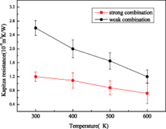
Figure 11. Kapitza resistance vs. the temperature.
Download figure:
Standard image High-resolution image
Figure 12. PDOS of the interfacial layer.
Download figure:
Standard image High-resolution imageThen the overlap factor of the material vibration spectrum is calculated. The calculation results are shown in figure 13. To avoid interference from the fixed layers, we chose the regions away from the fixed layers. The computational region of PDOS here is about 15 Å. We chose the structure with weak combination. Different from the interfacial transition layer, the low-frequency phonons account for the main heat transfer in monocrystalline silicon, while high-frequency phonons weaken with the increase of temperature. However, this indicates that the density of states of the materials on both sides are not only mismatch with each other, but also with the interfacial transition layer. The results show that with the increasing temperature, the overlap factor increases indicates that the heat transfer at the interface enhances, and the thermal resistance decreases, which is consistent with the previous discussion.
Figure 13. Out of plane PDOS of atoms at interface under different temperatures (a) 300 K (b)600 K.
Download figure:
Standard image High-resolution imageIn micro-nano devices, besides the normal thermal conduction perpendicular to the interface, the thermal conduction of composite materials parallel to the interface is also important to understanding the thermal conduction of the device. Researchers have paid attention to the anisotropy of Si/a-Si superlattices [15]. Such works can be the requirement of a new thermal management method (such as heat dissipation and insulation).
Figure 14 shows that the material has an obvious anisotropy. The system size is 20 a × 20 a × 20 a. The value of the anisotropy ratio is the in-plane thermal conductivity divided by out of plane thermal conductivity. The materials have different heat transfer capabilities out of plane and in-plane. It shows that the material has a certain heat insulation ability. Under the influence of the interface, the out-of-plane heat conduction is smaller than the in-plane heat conduction. With the increase in the proportion of amorphous silica, the anisotropy of the material will continue to increase. Although there is error interference, its overall trend does not change. However, due to the lower thermal conductivity of amorphous silicon dioxide, the increase of amorphous silica has little contribution to the total thermal conductivity. When it is parallel to the interface, single crystal silicon plays a major role in heat transfer, and the increase of amorphous ratio has little effect on the thermal conductivity of amorphous silica. In the in-plane heat transfer, the influence of interface on heat transfer is relatively small, and the main heat transfer still depends on crystalline materials. In practical applications, due to the existence of defects, especially the existence of the interface defects, the out-of-plane heat conduction may decrease, resulting in the increase of anisotropic ratio. It is suggested that the anisotropy can be changed by increasing interfacial thermal resistance.
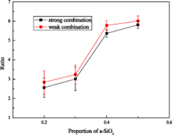
Figure 14. Thermal conductivity anisotropy of Si/a-SiO2.
Download figure:
Standard image High-resolution image3.3. The effect of strain on the thermal conduction
As mentioned in the first section, the strain can be used to adjust the thermal conductivity of materials at the micro/nano-scale. The strain application simulations of the two established models are carried out. Here all the strains are a cross-plane strain. All the engineering strains are performed under the deformation-control method with a strain rate of 0.001/ps [47, 48].
Figure 15 shows the effect of strain on the heat conduction of the material. It can be observed that the interfacial thermal resistance gradually increases from compression to tension. This is similar to the effect of strain on interface thermal resistance in the literature [48]. For the weak combination material, the strain effect is more obvious than that of the strong combination material, which indicates that it is easy to change the interface coupling strength when the coupling strength is weak. The main reason is the different characteristics of the interface. In the weak combination material, the range of the interface distance is obvious, and the interfacial thermal resistance depends on the interfacial distance greatly. Therefore, under the weak coupling strength, the thermal resistance changes significantly. At a certain tensile strain, the weak interface connection will fracture first, leading to material failure, which is not discussed here. When external strain, such as compressive strain, is applied, the relative decrease of interface thickness and the relative increase of the number of interfacial bonds are beneficial to phonon propagation. As a transition layer, the interface may enhance the thermal conduction of the interface, which is related to the density of the interface layer. Under compressive strain, the increase of interfacial density accords with the law in the literature [49], which is beneficial to the heat conduction. For the strong combination material, under compression strain, the compression degree of the interface spacing is smaller than that of weak combination material, so the results have no obvious change compared with those of weak combination material. Therefore, the enhancement of coupling strength is relatively weak and the enhancement of interface heat conduction is also weaker. As shown in figure 15(b), where the strain decreases, the thermal conductivity increases. The reason for the obvious change of weak combination material is similar to the interfacial thermal resistance under strain. From the error bars, the difference in compressive strain between the two materials will be reduced.
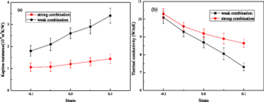
Figure 15. Strain effect on the thermal conduction of Si/a-SiO2 (a) Interfacial thermal resistance vs. strain (b) Thermal conductivity vs. strain.
Download figure:
Standard image High-resolution imageIt is not only the change of interfacial thermal resistance but also the materials on both sides of the interface that cause the change of thermal conductivity [17]. According to the literatures [4, 24], the changes of materials on both sides with strain are not consistent. Because the thermal conductivity of silicon makes the greatest contribution to the thermal conductivity of the whole material. The change of silicon from compressive strain to tensile strain is obvious. The change of overall thermal conductivity is reasonable in combination with the change of interface thermal resistance. Kinetic energy equation: is often used to analyze this phenomenon, where τph
represents phonon relaxation time and v represents phonon velocity. The variation of phonon relaxation time with strain in general solids was reported in the literature [23]. Due to the change of lattice vibration properties during stretching, the phonon velocity, and the phonon relaxation time of the material are reduced. This is consistent with our previous work [4].
is often used to analyze this phenomenon, where τph
represents phonon relaxation time and v represents phonon velocity. The variation of phonon relaxation time with strain in general solids was reported in the literature [23]. Due to the change of lattice vibration properties during stretching, the phonon velocity, and the phonon relaxation time of the material are reduced. This is consistent with our previous work [4].
The PDOS of the structure of compression and tension was calculated. The results are shown in figure 16. The computational regions of PDOS here is whole material. The material is strong combination material. The peak value of PDOS varies with different strains. In figure 16(c), through the partial enlargement drawing, the peak is around 15–16 THz. Compared with figure 9(a), this part is mainly contributed by single crystal silicon. The peak presents a red shift trend with increasing the tension. This means that the carrying energy of high-frequency phonons is reduced, and the heat transfer ability is reduced. On the contrary, the blue shift trend appears with the compression. The peak around 35 THz comes from the a-SiO2, which is similar to the phenomenon in monocrystalline silicon. In the low frequency of the whole vibration spectrum, there is no similar regular phenomenon. The results also show that strain has a great influence on high- frequency phonon, so it affects the heat transfer ability of the material.
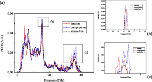
Figure 16. PDOS at compression and tension (a) Overall strain diagram of PDOS (b) and (c) Partial enlargement.
Download figure:
Standard image High-resolution imageThe overlap factors of the density of states under different strains are shown in figure 17. The computational regions of PDOS here are the same as in figure 13. The effect of strain may be reflected in increasing or decreasing the distance in the interface structure, thus reducing or increasing the strength of the interaction between the interfaces, that is, to reduce or to enhance the heat transfer performance. The other is that the compressive strain also enhances the shear interaction, thus increasing the contribution of phonons in the direction out-of-plane. The tensile effect is the opposite.
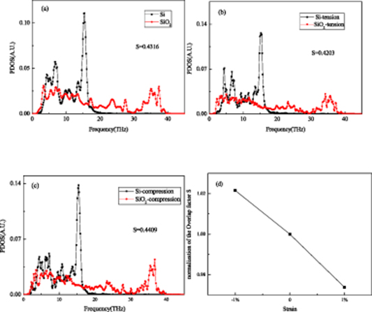
Figure 17. Out of plane PDOS of atoms at the side of interface under different strain (a) Strain-free (b) 1% tension (c) 1% compression (d) Normalization of overlap factors.
Download figure:
Standard image High-resolution imageChanging the applied strain is a method to way the heat conduction of heterostructure materials, which shows the anisotropy of thermal properties. Although there is error interference, its overall trend does not change. As shown in figure 18, the results show that the anisotropy increases with strain. The existence of strain not only affects the out-of-plane heat conduction but also affects the in-plane heat conduction. Therefore, under the action of external strain, the effects of strengthening and weakening in different directions are asynchronous. For example, tensile strain leads to a decrease in out-of-plane thermal conductivity. Based on similar laws, the in-plane thermal conductivity increases, and finally the the anisotropy of heat transfer increases. However, under the compressive strain, the anisotropy and the in-plane thermal conductivity also increases. It is speculated that the possible reason may be the size effect of the boundary. Although the interface coupling characteristics are different, the anisotropy is usually enhanced by strain.

Figure 18. Strain effect on thermal conductivity anisotropy.
Download figure:
Standard image High-resolution image
4. Conclusions
In this paper, we study the thermal conduction of Si/a-SiO2 with weak and strong combination in the interface using the MD simulation method. The existence and composition of the interface have a great influence on the thermal conductivity of the material. The interfacial thermal resistance is sensitive to system size and temperature and depends on interface strength. We can draw on the following conclusions:
- (a)The thermal resistance of the interface decreases with increasing temperature.
- (b)The structure shows great heat conduction anisotropy.
- (c)From compressive to tensile strain, the thermal resistance of the interface increases, the overall thermal conductivity of the material decreases, and the relative weak combination materials change more obviously. The applied strain changes the thermal conduction anisotropy of the Si/a-SiO2.
According to these conclusions, when considering thermal management and heat dissipation, we may design the silicon-based or any of silicon oxide micro/nano devices more precisely.
Acknowledgments
This work was supported by National Nature Science Foundation of China (Grant Number E51675420), Fundamental Research Funds for the Central Universities (Grant No. xzd012019020), Shaanxi Provincial Key Research and Development Program (Grants No. 2019GY-121).