
Abstract
Despite being known of for decades, the actual realization of memory devices based on the memristive effect is progressing slowly, due to processing requirements and the need for exotic materials which are not compatible with today's complementary-metal-oxide-semiconductor (CMOS) technology. Here, we report an experimental study on a Ge quantum wire device featuring distinct signatures of memristive behavior favorable for integration in CMOS platform technology. Embedding the quasi-1D Ge quantum wire into an electrostatically modulated back-gated field-effect transistor, we demonstrate that individual current transport channels can be addressed directly by controlling the surface trap assisted electrostatic gating. The resulting quantization of the current represents the ultimate limit of memristors with practically zero off-state current and low footprint. In addition, the proposed device has the advantage of non-destructive successive reading cycles capability. Importantly, our findings provide a framework towards fully CMOS compatible ultra-scaled Ge based memristors.
Export citation and abstract BibTeX RIS

Original content from this work may be used under the terms of the Creative Commons Attribution 4.0 license. Any further distribution of this work must maintain attribution to the author(s) and the title of the work, journal citation and DOI.
Information and communication technology has become ubiquitous in everyday life with ever growing potential in autonomous/self-learning (robotic) systems [1], Internet of Things [2], or artificial intelligence applications [3] to name just a few applications. However, upcoming, more sophisticated applications with high complexity will have demands beyond the capability of complementary-metal-oxide-semiconductor (CMOS) devices and require alternative information processing paradigms [4]. In this respect, neuromorphic computing is a rapidly growing area of computer science research that focuses on developing a computer built to mimic the human brain's neural networks. To implement such bio-inspired neuromorphic systems in hardware, numerous efforts have been made to realize scalable and power efficient artificial synapses [5], including resistive [6], magnet resistance [6, 7], phase-change [6, 8] or ferroelectric random access memories [9, 10].
More recently, attempts have also been made to develop non-CMOS based neuronal architectures using memristors, first reported by Chua et al [11–13]. These two-terminal devices can retain a state of internal resistance based on the history of applied voltage and current, emulating efficiently the synaptic functions [14] and sophisticated nanowire (NW) based devices have already been demonstrated [8, 15, 16]. NWs appeared to be attractive building blocks as the enhanced surface-to-volume ratio and confinement effects in these quasi-1D nanostructures can significantly alter their electrical properties with respect to bulk materials.
Aside from their physical advantages, NWs are also of particular interest to the semiconductor industry because their dimensions are of a technologically relevant scale and inroads have already been made towards incorporating them into mature Si platform technology [17–19]. NWs of various materials have already been integrated in memory devices making use of memristive behavior [20–23].
In this letter we demonstrate a memristive device, utilizing quantized charge carriers in ultra-scaled Ge NWs modulated by surface trap assisted electrostatic gating. The actual devices are about 2 µm long and comprise 18 nm thick single crystalline Ge NWs integrated in a back-gated field effect transistor (FET) architecture, as shown in figure 1. The notably thin Ge NWs used for this study have been synthesized by liquid injection chemical vapor deposition using diphenylgermane diluted in toluene at a growth temperature of 673 K [24]. Prior to NW growth, Ga growth promoters have been formed in situ by thermal decomposition of Ga(N(CH3)2)3 in toluene at 623 K. Applying this technique enables the growth of single crystalline, non-tapered Ge NWs of the required thickness below 20 nm. The high-resolution transmission electron microscopy (HRTEM) image in figure 1(b) reveals the perfect crystallinity of the NWs and a thin amorphous native Ge oxide shell. An additional HRTEM image of the Ge/GeOx interface is provided in figure S1 (https://stacks.iop.org/NANO/31/445204/mmedia). The fast Fourier transformation (FFT) pattern in the inset illustrates the growth along the  110
110 axis, which is the typical orientation for group IV NWs in this diameter regime [25]. For the actual devices, the Ge NWs are drop-casted onto a thermally oxidized highly p-doped Si substrate, which serves later as the common back-gate. Contacts to individual wires are fabricated by electron beam lithography, with removal of the native oxide shell by a 5 s dip in hydroiodic acid (14%) and subsequent 100 nm Al sputter deposition and lift-off processing as described previously [26].

Figure 1. (a) Schematic illustration of the Ge quantum wire device with false-color SEM image overlay of the Ge NW integrated in a back-gated FET architecture. The active channel length of the actual device is 1.8 µm. (b) HRTEM image and the corresponding FFT pattern of the about 18 nm thick NW revealing the excellent crystal quality and the  110
110 growth direction.
Download figure:
Standard image High-resolution imageFor basic electrical characterization, transfer characteristic measurements were performed in vacuum at 78 K using a liquid nitrogen flow cryostat. Figure 2 depicts the current response when the back-gate voltage VBG is swept from −30 V to + 30 V (red) and subsequently swept back to −30 V (blue) with a rather high bias voltage of VD = + 7 V. The intrinsic Ge NW exhibits ambipolor behavior with an ION/IOFF ratio of about 104 and distinct hysteresis effects. Thus, the current is not only dependent on VBG, but also the sweeping direction controlling the population of surface traps [27]. The thin native oxide layer at the Ge NW surface [28] with typical interface trap densities of 1012 to 1013 eV−1 cm−2 [29], provides a large number of such trapping states [30], which act as a highly efficient local gate [31] affecting the channel conductivity. Typical interface trap densities are in the range of 1012 to 1013 eV−1 cm−2, corresponding to roughly 0.1%–1% of the surface atoms [29]. Thus, for the actual devices with about 18 nm thick Ge NWs and a typical length of 1.8 μm about 1000 to 10 000 traps are involved determining the device behavior. The basic calculation of the number of traps can be found in the supplementary material.
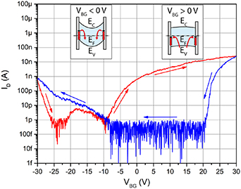
Figure 2. Typical transfer characteristic of the Ge quantum wire device measured for a bias voltage of VD = + 7 V in vacuum at a temperature of 78 K. The Ge quantum wire is 1.8 µm long and 18 nm thick. The insets visualize the trapping and de-trapping of surface traps as a function of the back-gate voltage.
Download figure:
Standard image High-resolution imageThe insets in figure 2 depict the trapping mechanism and the response with respect to the external electrostatic field. A high negative back-gate voltage (VBG = − 30 V) leads to a current of about 1 nA resulting from hole accumulation in the ambipolar NW. However, due to the imbalanced trap population with respect to the lowered Fermi level (figure 2, left inset), filled surface states begin to discharge over time to establish a new equilibrium resulting in lower band bending [32]. This de-trapping in combination with the less negative VBG results in a rapid decrease of the current by about three orders of magnitude. Continuous sweeping to positive gate voltages and discharged traps favors electron accumulation and induces a huge increase of the current, ultimately reaching 20 nA. However, again due to the imbalanced trap population (figure 2, right inset), now empty surface states are progressively refilled over time, repelling more and more electrons from the channel. Consequently, during the back sweep the current decreases and remains low, until the negative VBG induces again effective de-trapping accompanied with hole accumulation in the channel. Since this back-gate induced re-distribution of surface traps is kinetically controlled [33] a slower gate voltage sweeping rate would minimize the hysteresis effects [34]. However, as relaxation time constants for Ge NW devices are in the range from microseconds to several minutes for interface and oxide states [30, 35], one cannot completely avoid hysteresis effects for dynamic measurements within a reasonable time.
A further important and commendable feature is the overall low current for the notably high bias voltage of VD = + 7 V as a result of confinement effects in ultra-thin Ge NWs. For NWs with diameters about the Bohr radius, quantum confinement results in a band structure, composed of multiple 1D sub-bands each contributing a quantum unit of conductance of G0 = 2e2/h [36]. Due to the high carrier mobilities [37] and an exciton Bohr radius of aGe = 24.3 nm [38], Ge NWs represent a unique quasi-1D system, leveraging strong quantum confinement effects even at room temperature [27, 39]. For the actual 18 nm thick NWs, the current from the metallic Al contact-leads is re-distributed to a maximum of four sub-bands inside the Ge NW (see supplementary material) henceforth called quantum wire [40]. According to figure 2, we assume that for the maximum applicable back-gate voltage of VBG = + 30 V, under the given experimental conditions, we can only access one conductance channel [27]. Although the actual quantum wire is quasi-1D and thus shows confinement in two directions, its length is significantly exceeding the scattering mean free path of electrons in Ge [27, 41] and the conductivity is mainly determined by a parasitic series resistance related to scattering of charge carriers traversing the Ge channel.
The memristive behavior of the Ge quantum wire device shown in figure 3 is based on accessing conductance channels by controlling the trap population via electrostatic gating. To achieve a robust initial state, traps were completely discharged at room temperature by applying a back-gate voltage of VBG = − 30 V for 30 min and subsequently cooling the device to T = 78 K. Note that the device is always operated at a positive back-gate voltage of VBG = + 30 V, thus the current is predominantly driven by electrons as majority carriers.
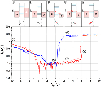
Figure 3. The main panel shows the memristive behavior of the Ge quantum wire, when sweeping the bias voltage forward and backward between −10 V and + 10 V for a fixed back-gate voltage of VBG = + 30 V at a temperature of 78 K. The upper panels show the conduction-band profiles of the Ge quantum wire and trap populations under characteristic biasing conditions. For simplicity the ensemble of traps is visualized by a single trap.
Download figure:
Standard image High-resolution imageThe conduction/sub-band profiles of the Ge quantum wire device and their relation to current-voltage characteristics and trap population under different bias voltages are shown in figure 3 and the respective insets. For clarity, the detailed Schottky barrier separating the sub-bands of the Ge quantum wire from the metallic Al contacts are not shown and only two sub-bands are indicated. Further, in analogy to FETs we will denote the left contact of the device as the source- and the right contact as the drain-electrode. Applying a negative bias of VD = − 10 V to the drain (point 1 in figure 3), a small reverse current flows due to leakage currents through surface states [42].
Notably, at this state the traps are empty due to the preceding de-trapping procedure. Sweeping VD towards 0 V, the drain level descends relative to the lowermost 1D sub-band and the leakage currents are reduced. For slightly positive bias, the current is in the opposite direction, remaining low as the drain level is still not resonant with the quantum wire sub-band. As thermionic emission over the barriers is strongly suppressed at 78 K, the OFF-state current of the device is practically zero (inset 2 of figure 3). If VD is increased above a threshold voltage of Vth = 5.5 V the drain level falls below the Ge quantum wire sub-band and electrons flow from the source into the sub-band and further into the drain (point 3 in figure 3) resulting in a steep increase of the current.
Simultaneously, electrons accelerated by the high electric field start now to fill up surface traps resulting in an effective negative gating of the quantum wire and thus a rise of the sub-bands.
This trap induced rise of the quantum wire's sub-bands leads to a persistent high current down to a bias voltage of about + 2 V during the voltage back sweep (point 4 in figure 3).
Finally, the current drops sharply when the drain's Fermi level rises above the lifted quantum wire sub-band (point 5 in figure 3). By the absence of hot electrons, the fast traps become discharged and the current at negative bias voltages is again limited by leakage currents through surface states.
Considering the application as a memory element, repeated reading cycles might alter the stored information due to the accumulative characteristic of a memristive device [43, 44]. For the Ge quantum wire a non-destructive reading process eliminates the need for a refreshment circuit [45]. For such non-destructive reading that can unambiguously distinguish resistive states, the bias voltage must be restricted to positive values. In this case the trap population is not affected during the reading process and the memristive state remains unaltered. Figure 4 demonstrates the readout for the OFF-state (empty traps—lower inset in figure 4). Independent of the sweeping direction only a few hundred femtoampere are flowing through the device if the bias voltage is kept below Vth. For the ON-state, the effective gating due to filled traps raises the sub-bands (upper inset in figure 4) and electrons flow from the source into the sub-band and further into the drain. If the voltage during the reading cycle is restricted to positive values the trapping remains unaffected and the ON-state conserved. Additional measurements regarding the cycle-to-cycle uniformity of the Ge quantum wire device can be found in the supplementary material (figures S2 and S3).
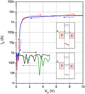
Figure 4. Memristive memory characteristic demonstrating non-destructive reading. I/V characteristic of the Ge quantum wire for positive VD for the ON- and OFF-state. The required charging of the traps to adjust the ON-state was achieved by a preceding writing cycle going once above Vth. The measurements were conducted with a positive back-gate voltage of VBG = + 30 V at a temperature of 78 K.
Download figure:
Standard image High-resolution imageThus, the Ge quantum wire device offers the feasibility of a memristive memory and introduces an adaptive read (0 < VD < Vth), write (VD > Vth) and erase (negative VD) method that may be used to realize a more resilient memory system.
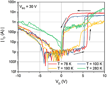
Finally, the impact of temperature on the resistive switching behavior of the Ge quantum wire device is elaborated. Figure 5 shows the I/V characteristics for a forward and reverse voltage sweep between −10 V and + 10 V at a back-gate voltage of VBG = + 30 V for various temperatures. Remarkably, up to about 190 K, the memristive behavior is retained. Changes of the performance with increasing temperatures manifest in a shift of Vth to lower voltages accompanied with a decrease of the ON/OFF ratio. At higher temperatures the Fermi and the sub-band levels are smeared out due to thermally enhanced electrons modifying Vth. Further, as trapping and de-trapping of electrons are kinetically limited processes [33], higher temperatures result in an increasingly faster transient re-distribution of surface charges. A detailed comparison of the transient device behavior at T = 80 K and T = 300 K can be found in the supplementary material (figure S4).
Figure 5. I/V characteristics of the quantum wire device at different temperatures between 78 K and 280 K for voltage sweeps from VD = − 10 V to + 10 V and back to −10 V.
Download figure:
Standard image High-resolution image
Notably, at room temperature, the memristive behavior disappears completely and the device remains in the ON-state. As shown in previous reports, at room temperature the surface traps of the Ge quantum wire are effectively filled up at positive gate voltages [27, 33] and remain permanently charged. For a negative VD, the reverse current increases as the permanently filled traps result in a lifting of the sub-band and to enhanced scattering.
Conclusions
In conclusion, we demonstrated a low footprint CMOS compatible Ge quantum wire device with memristive behavior and practically zero off-state current. Integrating the Ge quantum wire into a back-gated FET architecture, we demonstrated that individual current channels can be addressed directly by controlling the population of surface traps. By varying the bias voltage VD, the different modes of a classical memory system can be realized providing a platform which may pave the way for fully CMOS compatible neuromorphic computing.
Acknowledgments
The authors gratefully acknowledge financial support from the Austrian Science Fund (FWF): Project No. P29729-N27. The authors further thank the Center for Micro- and Nanostructures, TU Wien, for providing the cleanroom facilities. S.B. acknowledges funding in the Heisenberg Programme by the Deutsche Forschungsgemeinschaft (DFG, German Research Foundation) Grant BA 6595/1-1.
Author contributions
R.B. and M.S. contributed equally to this work. M.S. fabricated the samples. R.B. and M.S. conducted the electrical measurements. P.S. provided expertise on theoretical interpretations. S.B and M.S.S. synthesized the Ge quantum wires and performed the TEM experiments. A.L. conceived the project, contributed essentially to the experimental design. The manuscript was written through contributions of all authors. All authors have given approval to the final version of the manuscript.