

Abstract
In this study, random nanoscale rods (RNRs) with a double refractive index were fabricated via spin coating, dry etching, and sputtering, which are processes that are extensively applied in industry. With regard to optical properties, the RNRs with a double refractive index (RNRsD) exhibited a total transmittance that was >90% in the visible range and an optical haze in the range of 42%–50% at a wavelength of 520 nm. Organic light-emitting diodes (OLEDs) with RNRsD, where SiO2 was deposited on the RNRs via radiofrequency sputtering, exhibited an enhancement of 34.5% in the external quantum efficiency compared with OLEDs with the bare substrate. Furthermore, the color variation of the OLEDs with the optimal RNRsD with respect to a change in the viewing angle was improved from color coordinates of Δ(x, y) = (0.032, 0.034) to Δ(x, y) = (0.014, 0.014). Therefore, the proposed film can be used as a scattering layer for enhancing the light extraction and viewing angle of OLEDs by reducing the substrate mode light loss and changing the direction of light. In addition to using a low-temperature fabrication process that does not employ a photomask and a lithographic template, the proposed method is applicable to flexible devices because it uses a polymer and a thin inorganic film.
Export citation and abstract BibTeX RIS
1. Introduction
Organic light-emitting diodes (OLEDs) have been widely used for flat-panel displays and general lighting owing to their self-emitting characteristics, low power consumption, high response speed, high contrast ratio, excellent color gamut, and applicability to flexible devices [1, 2]. In spite of their internal quantum efficiency (IQE) of nearly 100% due to the use of phosphorescent materials [3–5], their external quantum efficiency (EQE) is ∼20% [6, 7]. The difference between the IQE and EQE is attributed to the light loss caused via the substrate, waveguide, and surface plasmon polariton modes, in addition to material self-absorption [8–10]. In the waveguide mode, traveling light is trapped owing to the different refractive indices of the constitutive layers, namely, indium tin oxide (ITO) (n = 2.0), organic layer (n = 1.7), and glass substrate (n = 1.5), of OLEDs. In the case of the surface plasmon polariton mode, emitted light is not reflected at the organic material/metal interface by the free electrons of the metal and propagates along the interface. It is essential to change the structure, shape, and thickness of the device for resolving this loss [11–14]. The substrate mode can be improved without changing the device, because the substrate mode is generated owing to the difference in refractive index between the substrate and the air. Therefore, researchers have attempted to find solutions for reducing the loss of the substrate mode and improving the optical properties of OLEDs.
Different approaches have been adopted with the aim of resolving the substrate loss, including microlens arrays (MLAs) [15–17], pyramids [18, 19], nanopillars [20], nanopatterns [21], a honeycomb structure [22], nanoparticles [23, 24], a high-index polymer with air voids [25], a porous polymer film [26], and self-catalytic-grown nanocones [27]. Among these textures, structures with the same pattern periodically, such as MLAs or pyramid structures, which are widely used for improving light extraction, can be fabricated via photolithography or lithographic templates. However, both of these methods are expensive and complex for mass production. Nanopillars and nanopatterns were fabricated via a simple method without masks or templates; furthermore, these exhibited random periodic structures. However, nanopillars had a small haze (as internal devices were inserted between the substrate and the anode), and it was difficult to apply nanopatterns to a glass substrate. Nanoparticles pose the risk of the aggregation of particles; in addition, the honeycomb and the rest of the structure were micro-sized, making it difficult to achieve optical effects such as diffraction and to apply a high resolution display with small pixel sizes. Even though nanocones are manufactured via a simple process without a photomask, the available substrates are limited, and multi-layer stacking problems are able to be caused by coefficient of thermal expansion owing to the high process temperature. In addition, the low total transmittance of nanocones in visible light is able to make an optical loss, and there is a disadvantage in external stress such as bending because nanocones was composed of only inorganic materials. In our previous work [28], we proposed a scattering layer using random nanoscale rods (RNRs) that was fabricated via spin coating and reactive-ion etching (RIE) at a low temperature; this layer was able to control the diffraction and scattering effects in the visible wavelength range owing to the distance between the closest rods, and the height of rods. However, this method had the limitation that the height and density were changed simultaneously; thus, new solutions were necessary to improve the scattering effects at a fixed density.
In this study, we further investigated the improvement of the optical properties of OLEDs using RNRs with a double refractive index (RNRsD) as a scattering layer. The RNRsD contained a dielectric layer, SiO2, and MgO or ZrO2 (deposited via magnetron sputtering) on the surface of the RNRs. The OLEDs with the optimal RNRsD exhibited an enhancement of 34.5% in the EQE and alleviation in the variation of the color coordinates with respect to changes in the viewing angle without spectral distortion which is observed in two-dimensional photonic crystal-based OLEDs [29, 30]. RNRsD can be widely utilized because they are fabricated using methods that have been already applied in a large scale in the display industry and because they involve low-temperature processes. Additionally, the pitch of hundreds-nanoscale, and thick polymer/thin oxide are compatible with a kind of solutions as a scattering layer for high-resolution and flexible displays.
2. Experiment
2.1. RNRsD fabrication
A schematic of the process flow for the fabrication of OLEDs with RNRsD is shown in figure 1. The glass substrate was cleaned via sequential sonication in acetone, methanol, and deionized water and was dried with a N2 gas gun. To achieve the target thickness, the polymer SU-8 (SU-8 2010, Micro-Chem.) and a thinner were mixed at a weight ratio of 1:1. The mixture was spin-coated onto a clean glass substrate at 2000 rpm. The coated substrate was baked on a hot-plate at 95 °C and exposed to conventional ultraviolet (UV) radiation (350–400 nm) at 130 mJ cm−2 for polymerization. The polymer film was transferred to an RIE chamber and was etched by O2 plasma at a radiofrequency (RF) power of 150 W, a working pressure of 70 mTorr, and O2 gas flow of 50 sccm for 10 min. The structure of the etched film was random columnar-like, with high aspect ratios and densities [31]. Without breaking the vacuum, the etched film was treated for 3 min with Ar plasma at an RF power of 200 W and a working pressure of 25 mTorr to obtain rods with the optimal density. The resulting RNRs exhibited a high total transmittance (>90%) in the visible range and an appropriate haze (∼40%) at a wavelength of 520 nm. For developing oxide thin films with various refractive indices, RNRs were subjected to RF magnetron sputtering. SiO2 (n = 1.46), MgO (n = 1.74), and ZrO2 (n = 2.21) thin films were deposited by using different sputtering targets. Because the deposition rate was different for each target, the process time was adjusted to standardize the deposition thickness. The deposition rates of SiO2, MgO, and ZrO2 were 3.74, 1.13, and 1.35 nm min−1, respectively, and different deposition times (16, 53, and 45 min) were applied to achieve identical target thicknesses. Finally, three types of scattering layers, i.e. 60 nm-thick SiO2, MgO, and ZrO2 on RNRs (denoted as RNRsD 1, RNRsD 2, and RNRsD 3, respectively), were obtained.

Figure 1. Process flow for fabricating OLEDs with RNRsD.
Download figure:
Standard image High-resolution image2.2. OLED fabrication
After the RNRsD were fabricated, ITO was deposited on the opposite side of the scattering layer via RF magnetron sputtering. The transparent ITO had a thickness of 180 nm and a sheet resistance of <10 Ω/□ as an anode for OLEDs. O2 plasma treatment of the ITO surface was conducted to remove organic contaminants and increase the work function. The prepared substrate was loaded in a thermal evaporator, and all the OLED components (organic materials and metals) were deposited under high-vacuum conditions (<2 × 10⁻⁶ Torr). The role and thickness of each of the layers of the OLEDs are as follows: a 40 nm-thick NPB (N,N'-bis(naphthalen-1-yl)-N,N'-bis(phenyl)-benzidine) layer and a 10 nm-thick TCTA (4,4',4''-tris(carbazol-9-yl)triphenylamine) layer for hole transport; a 30 nm-thick CBP (4,4'-bis(carbazol-9-yl)biphenyl) layer doped with 10 wt% Ir(ppy)3 (tris(2-phenylpyridine) iridium(III)) to function as the phosphorescent green emitting layer; 55 nm-thick B3PyMPM (bis-4,6-(3,5-di-3-pyridylph enyl)-2-methylpyrimidine) as the electron-transport layer; 0.7 nm-thick lithium fluoride as the electron-injection layer; and a 100 nm-thick Al layer as the cathode.
2.3. Numerical simulation
The optical effects of OLEDs with and without the scattering layer were simulated using commercial finite-difference time-domain (FDTD) software (Lumerical Solutions, Inc.). The simulation domain condition involved a perfectly matched layer on all sides to avoid the reflection of the electromagnetic waves at the edges of the structure, except for the metal cathode layer, where the metal boundary condition was used. The three dipoles (x-, y-, and z-polarized) were placed inside the emitting layer. The optical enhancement images of the OLEDs with RNRs and RNRsD relative to the reference structure were calculated as the ratio of the integrated electric-field intensities measured via a fixed far-field monitor. The height and width of the RNRs and RNRsD were set to the actual values considering the measured SEM images.
2.4. Measurements
The haze and total transmittance were measured via UV–visible–near-infrared spectroscopy (Cary 5000, Agilent Technologies Inc.). Cross-sectional and plane-view images of the RNRsD for determining the height and the density were obtained via scanning electron microscopy (S-4800, HITACHI High Technology Inc.). The densities of the rods were measured using an Image-Pro Plus 4.5. The refractive indices of the films were measured using a thin-film analyzer (F-20, Filmetrics, Inc.). The electrical characteristics (I–V) were measured using a Keithley 237 High Voltage Source-Measure Unit (Keithley Instruments, Inc.), and the electroluminescence (EL) intensity was measured in a dark box using a spectroradiometer (PR-670 Spectra Scan, Photo Research, Inc.).
3. Results and discussion
We investigated the use of RNRs as a scattering layer for improving the optical properties of OLEDs. The total transmittances of the RNR and RNRsD 1, 2, and 3 films were measured to be >90%, as shown in figure 2. Because of their high total transmittance, these films can be suitable as scattering layers without light loss arising from various phenomena such as backscattering or absorption. Their measured haze and specular transmittance were 42%–50% and 48%–55%, respectively, at a wavelength of 520 nm, and these values had the effect of escaping the waveguided light of the OLEDs in the substrate mode. The haze indirectly indicated the change in the optical path and was expressed by equation (1).

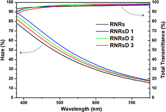
Figure 2. Haze and total transmittance with respect to the wavelength (visible range) for different RNRsD.
Download figure:
Standard image High-resolution imageAs shown in figure 2, the haze exhibited by RNRsD 1 was the largest in the scattering layer, even though the differences between the refractive indices of the RNRs and the dielectric layers were relatively small. This value means that the light whose optical path was changed by the SU-8 rod was emitted the most out using SiO2 thin film. In the case of flat thin films, the reflectance increases in proportion to the difference in refractive index under the same thickness and light absorption.
However, RNRsD 1, which was installed in the direction perpendicular to the substrate, exhibited a relatively facile movement of light between the rods and the air due to the gradient refractive indices [32].
Figure 3 shows the cross sections of the RNRs and RNRsD 1, 2, and 3, which had a random period and columnar structure with high aspect ratios. The average height was measured to be 1100 nm for the RNRs and 1200 nm for RNRsD 1, 2, and 3. The process conditions (deposition to a thickness of 60 nm on the flat substrate) increased the thickness of the rod-shaped structure because the angle between the substrate and the oxide target was 45° and the surface area at the top of the rods was increased. Scanning electron microscopy plane-view images of RNRsD 1 were analyzed using image-processing software. The density and average pitch of the rods were calculated to be 7.2 ea  and 420 nm, respectively (supplementary information figure S1 (available online at stacks.iop.org/Nano/31/335205/mmedia)). The average pitch of the rods was defined by the distance between the center of a certain rod and the center of the nearest rod and was derived from the density of the rods.
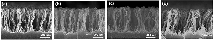
Figure 3. Cross-sectional scanning electron microscopy images of the scattering layers: (a) RNRs, (b) RNRsD 1, (c) RNRsD 2, and (d) RNRsD 3.
Download figure:
Standard image High-resolution imageThe optical enhancement and other phenomena of the OLEDs with RNRs and RNRsD 1, 2, and 3 were simulated using FDTD software. As shown in figure 4, the intensity of outcoupling light in the visible region with respect to the angles was obtained according to the scattering-layer conditions. Three orthogonal dipoles—parallel transverse-electric (TE) and parallel and perpendicular transverse magnetic (TM) dipoles [33]—were applied, and the simulation results reflected the sum of all the dipoles. The OLEDs fabricated in this study used an emitting layer that exhibited green phosphorescence in the primary wavelength range of 500–550 nm (supplementary information figure S2). As shown in figures 4(b)–(d), the outcoupling efficiencies of the OLEDs with RNRs and RNRsD 1 and 2 were higher than those of the reference devices in the green wavelength band. For RNRsD 3, the efficiency of the OLEDs in the green wavelength band was reduced. To identify the cause for the difference in the efficiency, the movement of light in the OLEDs and the scattering layer was analyzed by using the ability to observe over times in FDTD. The OLEDs with RNRsD 3 exhibited a larger amount of backscattered light in rods compared to all the other cases, including that of the reference OLEDs (supplementary information figure S3). This was presumably because of the increase in reflection or refraction when light was emitted from the rods into the air due to ZrO2 having a larger refractive index than the SU-8 materials [34]. In contrast, for RNRsD 1, the applied SiO2 (which had a smaller refractive index than SU-8), facilely propagated light between the rods and the air (supplementary information figure S4). This was attributed to the gradually decreasing refractive indices [35, 36]. In other words, the light of RNRsD 1 sequentially passed through 1.59, 1.46 and 1.0 refractive indices, while the light of RNRsD 3 passed through 1.59, 2.21 and 1.0. Figure 4(f) shows the numerical values of the light enhancement with respect to the wavelength for each scattering layer. In the green wavelength range of 500–550 nm, the average enhancement for the OLEDs with RNRsD 1, RNRs, RNRsD 2, and RNRsD 3 was 1.74, 1.62, 1.49, and 0.72, respectively. The simulation results indicate that to achieve an optimal light extraction of the OLEDs, it is advantageous to cover the rods with a thin film with a refractive index smaller than that of SU-8 (the rod material).

Figure 4. FDTD simulation results for OLEDs with different scattering layers: (a) reference (without scattering layer), (b) RNRs, (c) RNRsD 1, (d) RNRsD 2, and (e) RNRsD 3; (f) enhancement factor–emission wavelength graphs for the different scattering layers.
Download figure:
Standard image High-resolution imageFor five types of OLEDs—with RNRs, RNRsD 1, RNRsD 2, and RNR D 3 and without rods (Reference)—the changes in the optical characteristics with respect to the scattering layer were investigated. As shown in figure 5(a), the electrical characteristics of all the devices were almost identical, owing to the identical compositions and structures of the OLEDs and their simultaneous fabrication. However, the OLEDs with and without scattering layers exhibited different values for the luminance versus the applied voltage. Owing to the optical effect of the scattering layers, the luminance of the OLEDs with the scattering layers was higher than that of the reference OLEDs. Figure 5(b) shows the EQE with respect to the current density. The EQE of the OLEDs with RNRsD 1 (SiO2 thin film deposited on RNRs) was 8.2% at 50 mA cm−2. The OLEDs with RNRs, RNRsD 2 (MgO thin film deposited on RNRs), and RNRsD 3 (ZrO2 thin film deposited on RNRs) exhibited EQEs of 7.5%, 7.6%, and 7.6%, respectively. The OLEDs without a scattering layer exhibited an EQE of 7% at 50 mA cm−2. For the OLEDs with RNRsD 1, the enhancement of the EQE was 17.1% compared with the EQE of the reference devices in the normal direction. Because the scattering layers fabricated using RNRs and RNRsD 1, 2, and 3 also had the effect of reducing the substrate mode loss, the EQEs of the OLEDs with the scattering layers were increased in all four cases. However, the increase rate differed according to the scattering layer. This is because the light extraction of the OLEDs was affected by the haze values and refractive indices of the scattering layers. RNRsD 1 was considered to not only cause a larger scattering than the other layers owing to its high haze but also to facilitate light transmission owing to the small difference between the refractive indices of SiO2 and air. Figure 5(c) shows the current efficiency (CE) and power efficiency (PE) of the OLEDs with different scattering layers with respect to the luminance. The CEs of the OLEDs with RNRs, RNRsD 1, RNRsD 2, and RNRsD 3 were 24.0, 27.0, 24.4, and 24.4 cd A−1 respectively, and the CE of the OLED without a scattering layer was 22.3 cd A−1. The PE exhibited similar trends to the EQE and CE owing to the little difference in the electrical characteristics between the cases with and without the scattering layer.
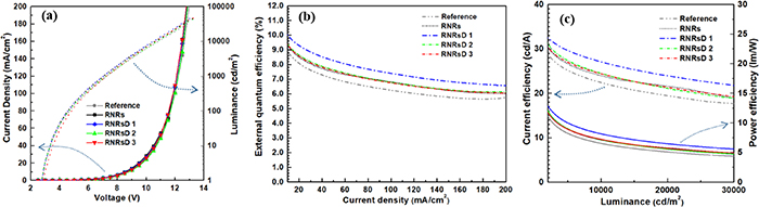
Figure 5. EL characteristics of OLEDs with different scattering layers: (a) J–V and L–V characteristics; (b) external quantum efficiency with respect to the current density; (c) CE and PE with respect to the luminance.
Download figure:
Standard image High-resolution imageFigure 6(a) shows the radiative intensity versus the viewing angle for OLEDs with and without scattering layers. For all the scattering-layer conditions, the luminance of the OLEDs was measured at a constant current of 1 mA and at intervals of 10° from 0° to 70°. The luminance of the reference OLEDs was 752 cd m−2 in the normal direction, and the OLEDs with scattering layers had different luminance values owing to the differences in the EQE. To compare the viewing-angle characteristics, the radiative intensity was normalized according to the luminance in the normal direction. Overall, the devices with a scattering layer exhibited a higher radiative intensity with respect to the viewing angle than the reference device which was similar to the Lambertian distribution. With regard to the measured radiative intensity at 40°, the OLEDs with RNRs, RNRsD 1, RNRsD 2, and RNRsD 3 exhibited improvements of 15.3%, 19.6%, 18.4%, and 16.5%, respectively, compared with the reference OLEDs. As shown in figures 5(a) and 2, the trends of the improvement of the radiative intensity and the haze value of the scattering layers were almost identical. Considering the variation of the radiative intensity with respect to the viewing angle, the OLED with RNRsD 1 exhibited a larger EQE enhancement (34.5%) than those with RNRs (18.6%), RNRsD 2 (23.5%), and RNRsD 3 (22.2%). The haze, total transmittance, and refractive indices, which were closely related to the EQE, are presented in table 1. Analyzing the variation of the CIE 1931 color coordinates for the viewing-angle range of 0° to 70° revealed that the difference between the maximum and minimum color coordinates for the OLEDs with RNRsD 1 was Δ(x, y) = (0.014, 0.014), while that for the reference OLED was Δ(x, y) = (0.032, 0.034), as shown in figures 6(b) and (c). Therefore, RNRsD 1 (with SiO2 deposited on RNRs), was an appropriate scattering layer for improving the optical properties of the OLEDs.

Figure 6. Optical characteristics of OLEDs according to the viewing angle for operation at 1 mA: (a) normalized angular luminance distribution; viewing-angle-dependent color coordinates in CIE 1931 (b) x and (c) y.
Download figure:
Standard image High-resolution image
Table 1. Haze, total transmittance, refractive index, the difference in the refractive indices of the scattering layers, and the enhancement in the EQE for different scattering layers.
| Haze (%) | Total transmittance (%) | R.I. at 520 nm | Δ R.I. | Enhancement in EQE (%) | |
|---|---|---|---|---|---|
| RNRs | 42.1 | 95.8 | 1.59 | — | 18.6 |
| RNRsD 1 | 50.4 | 96.7 | 1.59/1.46 | −0.13 | 34.5 |
| RNRsD 2 | 47.4 | 97.7 | 1.59/1.74 | 0.15 | 23.5 |
| RNRsD 3 | 45.1 | 96.4 | 1.59/2.21 | 0.62 | 22.2 |
4. Conclusion
We improved the optical properties of OLEDs using RNRsD as a scattering layer. The proposed fabrication method has many advantages; e.g. it involves a low-temperature process (<100°C), does not require photomasks, and is already widely used in industry. We investigated the effect of depositing thin films with different refractive indices on the surfaces of RNRs on the optical performance of the films. The optimal conditions yielded a 34.5% improvement in the EQE and an alleviation in the variation of the color coordinates and the luminance with respect to the viewing angle. Therefore, the RNRsD fabricated in this study can be used as a scattering layer for reducing the substrate mode loss. The proposed scattering layer is applicable not only to high-resolution displays, e.g. in virtual reality, owing to the nanosized rods, but also to flexible displays and lighting equipment owing to the rod-shaped structures of the organic and thin inorganic films.
Acknowledgments
This work was supported by a National Research Foundation of Korea (NRF) Grant funded by the Korean Government (MSIT) (No. 2019R1A2B5B01070286), the Ministry of Education (No. NRF-2017R1D1A1B03036520) and the Brain Korea 21 Plus Project in 2019.