
Abstract
Here we present a method to control the size of the openings in hexagonally organized BCP thin films of poly(styrene)-block-poly(4-vinylpyridine) (PS-b-P4VP) by using surface reconstruction. The surface reconstruction is based on selective swelling of the P4VP block in ethanol, and its extraction to the surface of the film, resulting in pores upon drying. We found that the BCP pore diameter increases with ethanol immersion temperature. In our case, the temperature range 18 to 60 °C allowed fine-tuning of the pore size between 14 and 22 nm. A conclusion is that even though the molecular weight of the respective polymer blocks is fixed, the PS-b-P4VP pore diameter can be tuned by controlling temperature during surface reconstruction. These results can be used for BCP-based nanofabrication in general, and for vertical nanowire growth in particular, where high pattern density and diameter control are of importance. Finally, we demonstrate successful growth of indium arsenide InAs vertical nanowires by selective-area metal-organic vapor phase epitaxy (MOVPE), using a silicon nitride mask patterned by the proposed PS-b-P4VP surface reconstruction lithography method.
Export citation and abstract BibTeX RIS

Original content from this work may be used under the terms of the Creative Commons Attribution 4.0 license. Any further distribution of this work must maintain attribution to the author(s) and the title of the work, journal citation and DOI.
1. Introduction
Block copolymer (BCP) lithography is one of several lithographic techniques which are top candidates for the next generation lithography with single-digit nanometer resolution and high throughput [1–6]. Block copolymers are suitable for formation of regular arrays of nanostructures and may even be used to achieve ultra-high density electronic devices, or other functional elements, on large areas at a relatively low cost. Unlike the 'top-down' high-resolution techniques, for example, extreme ultraviolet lithography, electron beam lithography or nanoimprint, BCP lithography is based on self-assembly of dissimilar polymer segments, that are covalently bonded to each other. The phenomenon of BCP self-assembly is a spontaneous organization of polymer molecules into well-defined regular features in the 5–100 nm range, driven by minimization of the free energy of the BCP-system.
In a block copolymer consisting of two different segments, the relative volume of the two, the length of the polymer chain, and the Flory-Huggins interaction parameter χ are the major factors influencing the type of self-assembly that could occur [7]. Furthermore, the relative volume of the segments, or blocks, can be controlled by introducing mixtures of solvent vapor [8], which are selective to the respective segments. By choosing a material system with a suitable, often high, χ, controlling the relative volume of the polymer segments, as well as the surface energy at the interfaces [9], and providing enough polymer chain mobility, it is possible to self-assemble the block copolymer into a regular pattern. The mobility is often provided using heat, as in thermal annealing [10], or using solvents, as in solvent vapor annealing (SVA) [8]. In BCP lithography, the most commonly used self-assembled pattern types are lamellae, horizontal cylinders, vertical cylinders in a hexagonal lattice, or spheres in a hexagonal lattice as one type of polymer block, all in a surrounding matrix of the other type of polymer block [5]. These periodically organized patterns can then be used in nanolithography applications.
A selective modification of one block in the BCP array would allow precise pattern transfer into a substrate. The modification could e.g. be removal of one block in dry etching [11], sequential infiltration synthesis [12], or so-called surface reconstruction utilizing a solvent selective to one of the blocks [13–15]. In BCP surface reconstruction, the self-assembled BCP is being exposed to a solvent selective to, most often, the minority block. This minority block will swell, whereas the majority block remains unchanged, as long as the temperature is kept below its glass transition temperature [13], i.e. the temperature where it begins to soften. As the minority block segments swell, the segments will migrate to the surface due to the confinement limited by the majority block [13]. When the solvent has evaporated, a BCP film with cavities will remain. Under such conditions, the minority block will wet the surface of the BCP layer [16], resulting in a topography suitable for lithography purposes. The solvent is commonly introduced by immersion into liquid, but can also be introduced as vapor [17].
The surface reconstruction of BCP has an advantage of being a simple, fully reversible process [13, 14] and can be combined with other process steps for pattern transfer, e.g. metal evaporation and dry etching [16]. It can also be used to improve the etching contrast between different blocks when one of the blocks is used as an etch mask [15]. Surface reconstruction has been demonstrated in other applications, such as formation of nano-composite membranes in poly(styrene)-block-poly(4-vinylpyridine) (PS-b-P4VP) films with pore sizes in the 30–50 nm range [18]. However, no systematic studies have been found to present the possibility to control the sizes of the openings after surface reconstruction and subsequent process steps. One exception is the latter study, which was briefly exploring the influence of surface reconstruction duration on pore size [18]. Thus, it is of a great interest to develop methods to control feature sizes of BCP films for a higher flexibility in the BCP lithographic patterning.
There are several advantages of using PS-b-P4VP, in BCP based nanofabrication, compared to other BCPs, such as poly(styrene)-block-poly(methylmethacrylate) (PS-b-PMMA). Firstly, it has a high χ [19], which enables patterns with small periodicities. Secondly, the P4VP easily interacts with metal or small molecules, forming possible routes for functionalization, inclusion of nanoparticles [20] or increased etch selectivity, and lastly, it is also possible to selectively infiltrate with alumina [21]. High χ BCPs are appropriate for high density pattern applications. One suitable application can be fabrication of templates for high-density III–V nanowire growth, to use in vertical nanowire transistors [22, 23]. Nanowire based devices could be advantageous in many different applications [24], and here BCP lithography could enable, not only an extremely high transistor density, but also a reduction of the nanowire diameter as compared to more commonly used lithography techniques, such as electron beam or UV lithography. The diameter reduction enables shorter gate lengths, which improves the performance of nanowire based field effect transistors (FETs) [25, 26]. Reducing the nanowire spacing will increase the transistor density, but also reduce parasitic capacitances allowing for high frequency operation.
In the present study, we report a method to control the size of the pore openings in a PS-b-P4VP film with hexagonally oriented vertical P4VP cylinders. The pores, with a diameter of 14–22 nm, are formed in a surface reconstruction process by immersion of the BCP into ethanol, which is a preferential solvent for P4VP. The size of the BCP openings increases with immersion temperature. To demonstrate the viability of our process for lithographic purposes, as well as for transistors, the reconstructed PS-b-P4VP was also used to pattern a silicon nitride template for indium arsenide vertical nanowire growth.
2. Experimental
We have identified the key steps in the processing to be surface reconstruction and polymer residue removal. The experimental part has therefore been divided into sample preparation, surface reconstruction, polymer residue removal and selective area metal-organic vapor phase epitaxy. A schematic overview of the fabrication process can be seen in figure 1.

Figure 1. Process scheme for block copolymer nanopatterning of a dielectric layer for selective area metal-organic vapor phase epitaxy.
Download figure:
Standard image High-resolution image2.1. Sample preparation
A 22 nm thick silicon nitride film was deposited on top of 1 × 1 cm2 Si substrates by plasma enhanced chemical vapor deposition (PECVD). The gases SiH4, N2 and Ar were used at 200 °C and 0.1 mbar. The deposition process took place in an inductively coupled plasma PECVD tool MicroSys 200 (Micro Systems GmbH, Germany). The sample surface was thereafter inspected in an optical microscope, and optionally in a scanning electron microscope (SEM). The substrate's contact angle to water was measured using Young-Laplace curve fit to a sessile drop, i.e. a droplet resting on a substrate.
Poly(styrene)-block-poly(4-vinylpyridine) (PS-b-P4VP), with a molecular weight of 50 k poly(styrene) and 17 k poly(4-vinylpyridine), and a polydispersity of 1.15 from Polymer Source Inc. (Canada), was then dissolved, to a 0.625 wt% solution, in a tetrahydrofuran (THF):toluene mixture in a 4:1 volume ratio. After annealing the substrates on a hotplate at 200 °C for 10 min for surface dehydration, and allowing them to cool down for 90 s, the polymer solution was spin-coated onto the substrates. The BCP coated substrates were thereafter baked on a hotplate at 120 °C for 3 min.
The polymer thickness, which was typically about 59 nm, was measured in a spectroscopic ellipsometer Wollam M2000VI or RC2 (Wollam inc. USA). Solvent vapor annealing was thereafter performed in a sealed beaker, containing a solvent vapor mixture from tetrahydrofuran:methanol in a liquid volume ratio of 9:1, for 4 h at room temperature. The samples were then left in ambient conditions for 10 min. The BCP films were also characterized, before SVA, using Bruker Dimension Icon (Bruker Inc. USA) atomic force microscope (AFM), operating in tapping mode, and analyzed using Gwyddion software (see figure 2(a)).
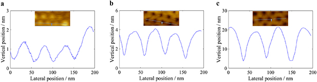
Figure 2. AFM height cross section profiles images and of PS-b-P4VP, (a) after spin-coating and baking, showing 1–2 nm protrusion of P4VP above the PS matrix, (b) after 60 min of surface reconstruction at 19 °C, showing 2–3 nm feature recess, and (c) after 60 min of surface reconstruction at 60 °C, showing 14–17 nm feature recess. Note that the AFM tip convolution effect result in smaller vertical dimensions than actual values.
Download figure:
Standard image High-resolution image2.2. Surface reconstruction
The surface reconstruction experiments in PS-b-P4VP films, were performed by immersing the samples into a beaker with ethanol. After immersion, the samples were blow dried in a nitrogen flow, and inspected in SEM Hitachi SU8010 (Hitachi, Japan) and/or AFM to measure the results of the surface reconstruction. To study the effect of time and temperature on PS-b-P4VP immersion in ethanol, we performed surface reconstruction for durations between 15 and 240 min at 18, 40 and 60 °C (see figure 3). The SEM data was later analyzed using the image analysis software ImageJ, and the mean pore diameter, mean pitch, size distribution, maximum and minimum values were calculated.
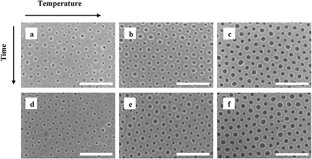
Figure 3. SEM top view images of PS-b-P4VP after surface reconstruction in ethanol at various temperatures and immersion durations: (a) at 18 °C for 15 min, (b) at 40 °C for 15 min, (c) at 60 °C for 15 min, (d) at 18 °C for 240 min, (e) at 40 °C for 240 min, and (f) at 60 °C for 240 min. The scale bar represents 200 nm.
Download figure:
Standard image High-resolution image2.3. Polymer residue removal
Remaining opening residues at the polymer-substrate interface were removed by an oxygen plasma ashing, performed in the inductively coupled plasma reactive ion etching (ICP-RIE) system Apex SLR (PlasmaTherm inc. USA). The tool operated at 3 mbar, an O2 flow of 30 sccm, 20 W RF, and 10 W ICP power for 90 s. The samples were thereafter inspected using SEM.
2.4. Selective area metal-organic vapor phase epitaxy
For the nanowire growth demonstration, we started with Si(111) substrates with epitaxially grown 270 nm thick tin (Sn) Sn doped indium arsenide (InAs) buffer layer [27]. A 22 nm silicon nitride layer was then deposited using PECVD. Prior to spin-coating of BCP films, the substrates were cleaned twice in acetone, thereafter in isopropanol using ultra-sonic treatment for three minutes each. After solvent vapor annealing and surface reconstruction of the PS-b-P4VP film in ethanol for 60 min at 60 °C, the opening residues were removed by ashing. To create a mask for epitaxy, the ICP-RIE system Apex SLR system was thereafter used to etch the silicon nitride layer with the BCP as an etch mask. This process used a working pressure of 10 mbar, a flow of CHF3 and N2, 20 and 80 sccm respectively, power levels of 14 W for RF bias, and 270 W for ICP, for 2 min. For the purpose of removing the polymer mask before epitaxial growth, the samples were processed in the Apex SLR ICP-RIE system at 3 mbar pressure, and an O2 flow of 30 sccm, 20 W RF power, and 10 W ICP power for 4 min. Prior to growth, the InAs native oxide removal was made by dipping the sample into 5% hydrofluoric acid solution for 15 s. Selective area metal-organic vapor phase epitaxy (MOVPE) of InAs nanowires was performed in a low-pressure close coupled showerhead (CCS) MOVPE (Aixtron GmbH, Germany) reactor, using precursors of trimethylindium (TMIn) and arsine (AsH3). First, 7 min of annealing in an arsine flow of 20 sccm at 600 °C was performed. The InAs nanowires were thereafter grown at a V/III precursor ratio of 5, during 4 min at 550 °C, and a pressure of 100 mbar, using hydrogen as a carrier gas. The structures were later characterized in SEM.
3. Results and discussion
The results and discussion section has been divided into BCP self-assembly, surface reconstruction, polymer residue removal, and selective area metal-organic vapor phase epitaxy, where the surface reconstruction and polymer residue removal are key processing steps.
3.1. BCP self-assembly
The spin-coating was performed from a solution of PS-b-P4VP in THF:toluene (4:1). It has previously been shown, that a THF content of 20–60 vol% in a PS-b-P4VP mixture microphase separate the BCP into vertical P4VP cylinders in a hexagonal pattern, when spin-coated onto silicon [28]. As THF has a higher evaporation pressure than toluene (see table 1), the evaporation from a solution of a higher percentage of THF should be faster, and a faster evaporation rate has earlier been simulated to promote vertical cylinders [29]. The chosen BCP mixture should therefore be appropriate for spin-coating. Our PS-b-P4VP initial layer thickness of about 59 nm was measured using ellipsometry, a value slightly larger than the bulk domain period length L0 of approximately 50 nm.
Table 1. Hildebrand's solubility parameters for polymers [30, 31] and solvents, and vapor pressures for solvents [32].
| Substance | Hildebrand's solubility parameter/(MPa1/2) | Vapor pressure/(mm/Hg) |
|---|---|---|
| Toluene | 18.3 | 21.9 |
| Tetrahydrofuran (THF) | 18.5 | 129 |
| Polystyrene | 18.3 | N/A |
| Poly-4-Vinylpyridine | 22.2 | N/A |
| Ethanol | 26.2 | 43.9 |
| Methanol | 29.7 | 97.3 |
Our AFM scans indicate that microphase separation occurs already after spin-coating, also on top of silicon nitride (see figure 2(a)). Self-assembly of PS-b-P4VP was possible on the silicon nitride substrate, without use of a surface energy modifying polymer brush layer. The surface energy of the substrate plays an important part in self-assembly of BCP thin films [9]. To illustrate the difference between a silicon wafer and the PECVD silicon nitride, contact angle measurements to water were made. A standard Si wafer had ∼37° contact angle to water, whereas the PECVD silicon nitride was more hydrophobic with a ∼51° contact angle to water. The BCP lithography process, without requirement of a brush layer, simplifies the whole processing scheme, as fewer steps are required.
Self-assembly of BCP occurs in grains, in neighboring regions having a pattern arranged (e.g. hexagonally) within each region [33]. This grain size can be enlarged, often referred to as improving the long-range order. A standard route to improve the long-range order is to extend the annealing time [34]. SVA in a mixture of toluene and THF have previously shown to enhance the long-range order of PS-b-P4VP pattern [16, 28]. We used THF and methanol for SVA, each selective to respective BCP block, and both have high vapor pressures, as can be seen in table 1. However, no obvious improvement of the long-range order was observed after 4 h of SVA. One plausible explanation for the poor improvement on the long-range order could be vapor leakage in the SVA system. Another possibility is a difficulty to overcome the polymer-surface interaction, as discussed by O'Driscoll et al [32]. We however suggest, that the long-range order could be improved further by implementing a SVA chamber using bubblers to introduce the vapor, and monitoring the BCP film swelling in-situ, as previously done by Gotrik et al [8]. It should thus be noted, that the surface reconstruction process can be performed also on non-equilibrium BCP structures, where the P4VP block sizes are irregular, and the ordering low. The irregularity and low ordering can be explained by the high polydispersity, the substrate-polymer interaction and the choice of annealing process.
3.2. Surface reconstruction
Our results demonstrate that ethanol immersion of PS-b-P4VP at 18 and 40 °C had no, or very limited, tendency for pore diameter to increase with time, within the four-hour immersion time (see figure 4(a)). We did observe a weak dependence of the PS-b-P4VP thin film pore diameter with time for 60 °C ethanol immersion temperature within the time frame 30 to 240 min, resulting in an increase from 22.2 to 24.3 nm on average (see figure 4(a)). Our conclusion is that the effect of surface reconstruction time on the pore diameter is fairly small. Our results do not necessarily contradict the results from Liu et al, who created pores in PS-b-P4VP in a higher molecular weight BCP, with a higher fraction of P4VP, by first spin-coating a solution of the BCP in toluene, which gave micellae with P4VP cores. They thereafter immersed the sample into 60 °C ethanol, a preferential solvent for P4VP. Their study concluded that the BCP membrane pore diameter increased with immersion time up until 2 h duration [18]. However, Liu et al did not report specific numbers of the increase in pore size with time, but instead referred to SEM images taken.

Figure 4. PS-b-P4VP pore diameter on SiNx/Si (a) to ethanol immersion time, (b) to ethanol immersion temperature, and (c) distribution after one-hour immersion, where the lines are to guide the eye (an approximation of a bell curve, adapted to measured mean and sigma values). The error bars represent ±σ, around the mean values of each point, and in (b) only the extreme values of each group are marked.
Download figure:
Standard image High-resolution imageThe average pore diameter increased with temperature, though, ranging from 13.9 nm at 18 °C immersion to 22.2 nm at 60 °C immersion, as shown in figure 4(b). When using 70 °C immersion temperature, the morphology shifted to a film without pores, which would be highly unfavorable for any subsequent pattern transfer. Furthermore, our data illustrate that the pore size distribution had a tendency to increase with temperature, as can be seen in figure 4(c). The pore size distribution should also be possible to lower by using a BCP with a lower polydispersity.
The mean pitch has a tendency to increase with temperature, although the data for 15 min immersion time deviates from this trend (see figure 5(a)). The pitch, or the pattern periodicity, is here defined as the distance between neighboring pore centers. At lower temperatures, the pitch decreases with time, whereas the pitch increases somewhat with time at higher temperatures, as seen in figure 5(b). It is likely that, with time, the self-assembly gets closer to its equilibrium state, although the mobility of the PS block should be very limited at lower temperatures. It should, however, be pointed out, that the main purpose of surface reconstruction is to open pores. Furthermore, the standard deviation, σ, shows a tendency to decrease slightly with time, e.g. from 4.9 nm at 15 min to 4.3 nm at 240 min and 60 °C (see distribution in figure 5(c)), but shows no clear dependency on temperature. It should be noted, that due to less contrast in the SEM images, both the pitch and pore size data analysis of samples from 15 min immersion time are less accurate. AFM measurements verified that surface reconstruction creates a topography of pores (see figures 2(b) and (c)). However, a thin polymer layer wets the entire substrate, which needs to be taken into consideration in subsequential lithography processing. Its existence is supported by SEM cross section images.

Figure 5. PS-b-P4VP pattern pitch on SiNx/Si (a) to ethanol immersion time, (b) to ethanol immersion temperature, and (c) distribution after immersion at 60 °C, where the lines are to guide the eye (an approximation of a bell curve, adapted to measured mean and sigma values). The error bars represent ±σ, around the mean values of each point, and in (b) only the extreme values of each group are marked.
Download figure:
Standard image High-resolution imageOur data show, that using a suitable ethanol immersion temperature can control the resulting PS-b-P4VP pore sizes, for BCP with a fixed molecular weight. Surface reconstruction can thus function as a method of tunable block copolymer lithography for nanofabrication. It should, furthermore, be noted that changes in the substrate's surface energy may alter the resulting pore sizes, likely due to the substrate-polymer and polymer-solvent interaction. The trend of increasing pore size with temperature do, however, remain, in line with earlier investigation [35]. Furthermore, has the repeatability of the surface reconstruction process has been verified, on silicon nitride coated silicon substrates (see supplementary data (available online at: stacks.iop.org/Nano/31/325303/mmedia)). Although our study did not focus on large area uniformity investigation, BCP lithography is easily applied over large areas, and the performed processes should not change significantly when moving to large area applications.
We have performed surface reconstruction of PS-b-P4VP in ethanol. Could alternative solvents be useful for surface reconstruction? O'Driscoll et al concluded that reversal of micellae in a film, spin-casted from PS-b-P4VP in toluene, occurs after exposure to ethanol, and that it could be explained by the Hildebrand solubility parameters [32], as P4VP is preferentially soluble, and swells in it (see also table 1). Selective swelling of one block will, furthermore, shift the relative volume of the two blocks [36, 37], which may affect the morphology. In contrast, non-preferential, neutral solvents would rather swell both blocks, and accumulate at the block-to-block interface [36]. Also relevant, is that a solvents selectivity will often change with temperature [38]. Several factors are, thus, of importance when discussing alternative solvents, and block selectivity is perhaps one of the more relevant.
The consequence of using a solvent selective to P4VP, is swelling of the block, effectively lowering its glass transition temperature, which should facilitate material transport of the P4VP. Using a higher surface reconstruction temperature, should further facilitate material transport, as the material then softens even more. This might explain why a higher surface reconstruction temperature gives larger BCP pore sizes. At 70 °C, the morphology shifted to a film without pores, why we suspect that also the PS block softened enough at this temperature to allow larger material transport. It can furthermore be noted, that an increased temperature corresponds a decrease in the interaction parameter χ [5].
In BCP in solution, it has previously been found that the lamellae domain spacing was highly dependent on the selectivity of the solvent [36], where an increasing dilution of a highly selective solvent increased the domain spacing, whereas a neutral solvent decreased it. It is possible, that the domain spacing of a spin-casted film also could be affected by solvent selectivity, provided sufficient chain mobility is added. Our experimental results of a slightly increasing pitch with increasing surface reconstruction temperature, could originate from several different mechanisms. It could potentially be a result of increasing BCP volume with temperature, an effect equivalent to a change in dilution with temperature, or possibly an effect of selectivity shift with temperature. Investigation of which of these mechanisms are responsible is, however, out of scope of this paper.
3.3. Polymer residue removal
To show how the BCP pattern can be used for lithography purposes, we performed ashing at a vertical etch rate of 18 nm PS-b-P4VP per minute to remove any remaining polymer residues at the bottom of the features. Figure 6(a) shows the pores after ashing. We have performed ashing of samples surface reconstructed at different temperatures for different durations, to investigate the resulting pore size (see figure 7). The duration of surface reconstruction was found to be of no significance to the pore size after ashing, resulting in a large process window. The pore size after ashing increased with surface reconstruction temperature, why we conclude that adjusting the BCP openings by surface reconstruction temperature is a viable lithography method.
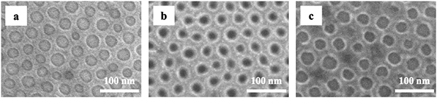
Figure 6. SEM images of PS-b-P4VP defined features, (a) after ashing, (b) after silicon nitride etching, and (c) after diluted hydrofluoric acid cleaning.
Download figure:
Standard image High-resolution image
Figure 7. PS-b-P4VP pore size on SiNx/Si to ethanol immersion temperature. Lower data set showing sizes after surface reconstruction at three different temperatures, for varying durations. The upper data set shows pore sizes after ashing. The error bars represent ±σ, around the mean values of each point, where only the extreme values of each group are marked.
Download figure:
Standard image High-resolution image3.4. Selective area metal-organic vapor phase epitaxy
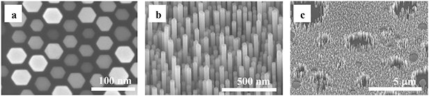
To demonstrate growth of vertical indium arsenide (InAs) nanowires from features defined by surface reconstructed BCP lithography, we created a template in silicon nitride. After ashing of the BCP, a dry etching of silicon nitride was performed at a vertical etch rate of 13 nm min−1, using the BCP as an etch mask, to create this template. The silicon nitride feature profile was then of a low wall angle (see figure 6(b), and supplementary data). After 15 s HF(5%) dip, the average diameter of the silicon nitride openings had increased by 2 nm from the surface reconstruction openings (see figure 6(c)). As InAs preferentially grows in <111> B directions [39], the openings in the amorphous silicon nitride down to the crystalline (111)B substrate should favor vertical growth for suitable process conditions. Furthermore, the nanowire lateral size should depend on the size of the opening in the amorphous mask [40]. Selective area MOVPE was successfully utilized to produce nanowires (see figure 8). The InAs nanowires were grown in a hexagonal pattern of approximately 50 nm pitch, on average sized 32 nm at the top, across the slowest growing facets, which is 7 nm larger than the openings in the created silicon nitride mask. A more detailed investigation on size change during pattern transfer and nanowire growth is underway. The nanowire length varied among the nucleated nanowires, but was in the order of hundreds of nanometers. The InAs growth occurred, both as larger island growth in specific areas, and as nanowires in the vertical direction in other areas, and the process steps were thus not yet fully optimized. Some of the island growth, which occurred in regions, might be originating from local variations in the silicon nitride layer, or from BCP thickness variations, which affects the BCP self-assembly, and therefore also the pattern transfer, negatively. Also, Huang et al have previously reported varying InAs nanowire length using GaAs substrates with a SiNx mask, and PS-b-PMMA patterning, with a nanowire growth yield of up to 32%. They also reported island growth areas, as well as areas without growth [41]. Increasing the vertical nanowire yield above e.g. three standard deviations, or 99.7%, for full area patterned wafers might be challenging due to defectivity issues, but if the growth is restricted to a smaller area, e.g. by lithographically masking out areas to be excluded in epitaxy, the yield will likely increase.
Figure 8. SEM images of selective area grown InAs nanowires using silicon nitride template, where (a) is top view, (b) is tilted view, and (c) is also showing island growth and areas without growth in tilted view.
Download figure:
Standard image High-resolution image
4. Conclusions
We demonstrate, for the first time, that the diameter of the pores in cylindrical hexagonally-organized block-copolymer thin films of poly(styrene)-block-poly(4-vinylpyridine) (PS-b-P4VP) on a SiNx/Si substrate can be controlled by altering the surface reconstruction temperature. A surface reconstruction process in ethanol results in an increase of BCP pore diameter from 13.9 to 22.2 nm as the temperature is raised from 18 to 60 °C. However, we found no significant changes in the pore diameter as a function of the surface reconstruction time. A subsequent ashing process confirmed this finding, demonstrating a large process window. Finally, we demonstrated epitaxial growth of III–V nanowires, by performing a high-resolution pattern transfer to create a template mask of SiNx, using surface reconstructed BCP lithography. The obtained results should be of use within BCP-based nanofabrication of high density features, and for applications such as III–V vertical nanowire transistors.
Acknowledgments
We acknowledge Björn Landeke-Wilsmark for his contributions on block copolymer processing in the initial stages of this work, Mariusz Graczyk for development of silicon nitride deposition, Mattias Borg and Harald Havir for their contribution on development of the silicon nitride etching, and Anders Kvennefors and Dmitry Suyatin for valuable discussions regarding reactive ion etching. This study was financially supported by the Swedish Foundation for Strategic Research, project SSF RIF14-0090, and from EU's H2020 Framework Program, in project Nanoscience Foundries and Fine Analysis—Europe (NFFA-Europe), project number 654360. We also acknowledge financial support from the Royal Physiographic Society of Lund, NanoLund at Lund University and MyFab.