
Abstract
Artificial intelligence (AI) has the ability of revolutionizing our lives and society in a radical way, by enabling machine learning in the industry, business, health, transportation, and many other fields. The ability to recognize objects, faces, and speech, requires, however, exceptional computational power and time, which is conflicting with the current difficulties in transistor scaling due to physical and architectural limitations. As a result, to accelerate the progress of AI, it is necessary to develop materials, devices, and systems that closely mimic the human brain. In this work, we review the current status and challenges on the emerging neuromorphic devices for brain-inspired computing. First, we provide an overview of the memory device technologies which have been proposed for synapse and neuron circuits in neuromorphic systems. Then, we describe the implementation of synaptic learning in the two main types of neural networks, namely the deep neural network and the spiking neural network (SNN). Bio-inspired learning, such as the spike-timing dependent plasticity scheme, is shown to enable unsupervised learning processes which are typical of the human brain. Hardware implementations of SNNs for the recognition of spatial and spatio-temporal patterns are also shown to support the cognitive computation in silico. Finally, we explore the recent advances in reproducing bio-neural processes via device physics, such as insulating-metal transitions, nanoionics drift/diffusion, and magnetization flipping in spintronic devices. By harnessing the device physics in emerging materials, neuromorphic engineering with advanced functionality, higher density and better energy efficiency can be developed.
Export citation and abstract BibTeX RIS

Original content from this work may be used under the terms of the Creative Commons Attribution 3.0 licence. Any further distribution of this work must maintain attribution to the author(s) and the title of the work, journal citation and DOI.
1. Introduction
After more than 50 years from its start, the evolution of the microelectronic industry can no longer be adequately described by the Moore's law of scaling the transistor size [1]. For years, making the transistor smaller has meant improving the density, performance and power consumption of a digital circuit. More recently, transistor miniaturization has been replaced by more advanced approaches, such as the introduction of high-k materials for the gate dielectric [2], the adoption of enhanced transistor layouts such as trigate structures [3], and possibly in the future the use of alternative switch concepts [4]. Most importantly, new computing methodologies such as quantum computing [5], stochastic computing [6], and analogue computing [7] are currently under scrutiny to overcome the main limitations of digital circuits.
Among the novel computing approaches under investigation, neuromorphic computing is probably the most promising. Neuromorphic engineering defines the development of systems that emulate the human brain to achieve high energy efficiency, parallelism, and ability in cognitive tasks, such as object recognition, association, adaptation, and learning. The concept of neuromorphic systems is not novel, being first introduced in the 1980s as a branch of analogue circuit engineering [8]. The original neuromorphic concept is based on analogue circuits with extensive use of subthreshold-biased transistors, as a means to minimize the energy consumption and exploit the similarity between carrier diffusion in the transistor and atomistic transport in the ionic channel of a biological synapse [9]. During the years, analogue circuits for neurons and synaptic functions have been proposed [10], and led to the development of general-purpose chip demonstrators [11]. Although the complementary metal-oxide semiconductor (CMOS) technology is essential to enable the integration of large-scale neuromorphic systems, it does not easily provide some of the inherent features of the neurobiological network, such as the long-term plasticity, the stochastic behavior, and the ability to update internal variable, such as synaptic weight and membrane potential, as a function of spike timing and frequency.
In the last 10 years, there has been a wide exploration of new devices as technology enablers of neuromorphic computing. The class of emerging memories is very promising for neuromorphic computation, thanks to the ability to store analogue values in nonvolatile way, combined with the extremely small device size [12, 13]. Also, emerging nonvolatile memories feature a unique device physics that can provide a broad portfolio of functions, such as time-dependent dynamics, low-voltage operation and stochastic switching. Most importantly, emerging memories naturally enable the so-called in-memory computing paradigm, where data are processed directly within the memory, thus with no need for any energy- and time-consuming transfer to/from the memory circuit [14]. Note, in fact, that our brain is essentially built on the concept of in-memory computing, where neurons and synapses serve the function of both memory and computing elements [15, 16]. Memory devices can also be organized with array architectures, such as the crosspoint array [17, 18] and the one-transistor/one-resistor (1T1R) array [19, 20], which strictly resemble the structure of a neural network, where each memory conductance plays the role of a synaptic weight [14, 21]. For all these reasons, emerging memories, also known as memristors, are considered a strong contender for the implementation of high-density, low energy neuromorphic circuits.
This work provides an overview on the emerging devices for neuromorphic computing with an emphasis on nonvolatile memories for synaptic and neuron applications. First, the emerging memory devices that are currently investigated for neuromorphic applications are reviewed in terms of the physical switching mechanisms and inherent performance in terms of speed, multilevel operation, and scaling. Then, the synaptic concepts based on emerging memories are described, referring to various types of neural networks and learning rules, aiming at either supervised or unsupervised training. Examples of neural networks implementing brain-inspired learning rules for pattern recognition are shown. Neuron circuits employing emerging devices are then reported, including various classes of oscillating, accumulating, and stochastic neurons. Finally, examples of neural networks combining emerging neuron and synaptic devices are presented. The open challenges and remaining gaps for the development of this field are finally summarized.
2. Neuromorphic networks
Neuromorphic engineering aims at developing circuits that compute as the human brain. An essential feature of any neuromorphic circuit is the neural network architecture, where data are sent by neuronal terminals through a highly-parallel net of synaptic paths. The concept of neural network can be traced back to the neuron model proposed by McCulloch and Pitts, who for the first time described the neuron as a mathematical function of the synaptic inputs [22]. The prototypical version of the neural network is the perceptron, which is capable of recognizing linearly separable classes of objects [23]. More advanced schemes of neural networks, generally referred under the term of deep learning, have been first proposed [24] and more recently led to an increased interest [25] for the outstanding performance in object and face recognition, even matching or surpassing the human capability [26]. More brain-inspired concepts have been developed, such as the concept of reinforcement learning which enables self-adaptation within a neural network as for the human brain. For instance, it has been shown that a neuromorphic platform can learn to play videogames [27] or the ancient game of Go [28] by iteratively playing games, and autonomously learning from successes and failures. Most of these achievements were however obtained by running software programs in digital computers, taking advantage of the outstanding performance of advanced central processing units (CPUs) and graphics processing units (GPUs) to expedite the supervised training for setting the synaptic weights within the network. The digital computation is extremely power hungry, while lacking any similarity with the brain architecture. To realize energy-efficient, scalable neuromorphic hardware systems, it is necessary to mimic the brain from its very fundamental architecture, communication and computation schemes.
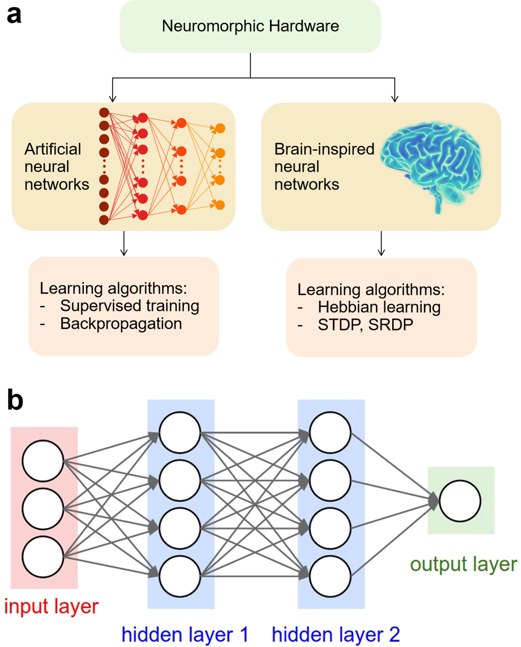
Figure 1(a) schematically illustrates the two basic types of neuromorphic hardware, namely artificial neural networks (ANNs) and brain-inspired networks. These types of hardware differ mainly from the methodology for training the network synapses, while sharing the general neural network architecture. In ANN, the deep structure with many layers can only be trained by supervised learning algorithms such as the backpropagation scheme [25]. On the other hand, brain-inspired networks adopt learning rules which are derived from the neurobiological systems, such as Hebbian learning and the spike-timing dependent plasticity (STDP) [29, 30]. Note that, although ANNs are also inspired by the brain, the training algorithms such as the backpropagation technique are not, which justifies the nomenclature in figure 1(a).

Figure 1. Illustrative sketch of neuromorphic hardware options. (a) Neuromorphic hardware can be implemented via both artificial neural networks (ANNs) and brain-inspired neural networks. These two approaches rely on a different set of algorithms and learning rules, e.g. the backpropagation algorithm in ANNs, or the spike-timing dependent plasticity (STDP) in brain-inspired concepts. (b) A generic neural network, organized as neuron layers where each neuron is connected by synapses to neurons in the previous layer, and the next layer. The number of layers defines the 'depth' of the neural network.
Download figure:
Standard image High-resolution imageBoth bio-inspired networks and ANNs in figure 1(a) rely on the fundamental neural network structure of figure 1(b). This shows a fully-connected multilayer perceptron (MLP), which is the prototypical network for deep learning for object, face, and image recognition. The network consists of layers of neurons, including (i) input neurons, providing the input pattern of information, (ii) output neurons, providing the solution to the classification problem, and (iii) a number of hidden layers, where the intermediate solutions from input to output variables are found. Each neuron in the network can execute a summation or integration of the input signals, followed by a nonlinear operation, such as logistic or sigmoidal function. The output of each neuron is then transmitted to neurons of the next layer via synaptic connections, which multiply the signal by a proper synaptic weight. The network can have a feedforward structure, meaning that the information is sent from the input layer to the output layer, or a recurrent structure, where a feedback connection is also present from a neuron layer back to another preceding layer. One example of recurrent network is the Hopfield network, where a layer of neurons sends information toward themselves through a single layer of synaptic connections [31]. Information among neurons is generally sent via synchronous or asynchronous spikes.
3. Emerging memory devices
To implement the neural network of figure 1(b) in hardware, it is necessary to identify the most suitable circuit to represent the neuron and synapse function. In this scenario, emerging memory devices play a major role, since they can provide added functionality to the conventional CMOS technology, such as the ability to implement analogue, nonvolatile memory within a nanoscale region on the chip. The emerging memory also enables the in-memory computing approach where data are processed in situ [14]. Emerging memory devices can be divided in two categories, namely 2-terminal devices and 3-terminal devices, as illustrated in the following.
3.1. 2-terminal devices
Figure 2 summarizes the 2-terminal devices that are currently studied for applications in neuromorphic computing circuits [14]. These include the resistive switching random access memory (RRAM), the phase change memory (PCM), the spin-transfer torque magnetic random access memory (STT-MRAM) and the ferroelectric random access memory (FeRAM). These memory devices all share the same basic structure, with an insulator and/or active material sandwiched between 2 metal electrode layers. The application of external voltage pulses to the device will induce a change in a characteristic property of the memory device, which can be sensed as a variation in the resistance, or the electric/magnetic polarization. As a result, one can program, erase and read the memory by electrical operations on the memory device, which can retain the written state for long time, e.g. 10 years at elevated temperature. This is similar to the conventional nonvolatile Flash technology, which has been a consolidated memory device with extremely high density for the last 30 years [32, 33]. However, Flash memory relies on the storage of charge within a floating gate of a MOS transistor, whereas all the emerging memory concepts in figure 2 are based on material properties which can be changed by electrical operations. Thanks to the charge-free material modification, the scalability of the emerging memory is generally superior to Flash memories.

Figure 2. Illustrative sketch of the memory devices that are considered for in-memory computing, including neuromorphic computing. (a) A resistive switching random access memory (RRAM), and (b) its representative current–voltage indicating bipolar switching between a low resistance state (LRS) and a high resistance state (HRS). The switching process originates from the ionic migration across a filamentary path within the metal-insulator-metal (MIM) stack of the RRAM. (c) A phase change memory (PCM), and (d) its resistance–voltage (R–V) characteristic, where the resistance drop at low voltage is due to the crystallization, and the resistance increase is due to melting and amorphization of the phase change material. (e) A spin-transfer torque magnetic random access memory (STT-MRAM), and (f) its R–V characteristic, where the transition between parallel (P) and antiparallel (AP) states dictates variations of the resistance. (g) Ferroelectric random access memory (FeRAM), and (h) its polarization–voltage characteristic, indicating the typical hysteresis of ferroelectric insulating layer in the MIM stack. Reprinted with permission from [14]. Copyright 2018 Springer Nature.
Download figure:
Standard image High-resolution imageThe RRAM device in figure 2(a) consists of a metal-insulator-metal (MIM) structure, where the insulating layer can change its resistance from relatively large, in the high resistance state (HRS), to relatively low, in the low resistance state (LRS) [34–36]. The resistance change generally takes place at a localized region within the insulating layer, referred to as conductive filament (CF). To form the CF, RRAM is subjected to a preliminary operation, called forming, consisting of a soft dielectric breakdown to induce a local decrease of resistance. The set process allows to operate the transition from the HRS to the LRS, whereas the reset process is responsible for the transition from the LRS to the HRS. The set and reset processes are both induced by the application of voltage pulses, which can have the same bias polarity, in the case of unipolar RRAM [37, 38], or, most typically, the opposite bias polarity, in the case of bipolar RRAM. Figure 2(b) shows a typical current–voltage characteristic for a bipolar RRAM, indicating the set transition as a steep increase of the current at the positive set voltage Vset and the reset transition to the HRS starting at the negative voltage Vreset. The set and reset transitions are generally explained in terms of defect migration within the CF: for instance, the application of a reset voltage across the CF leads to drift and diffusion of the ionized defects, such as oxygen vacancies and metallic impurities, resulting in a retraction of the CF toward the negatively-biased electrode [39]. The CF retraction causes the formation of a depleted gap with low concentration of defects, hence high resistivity, which is responsible for the increase in resistance in the reset transition. Applying an opposite voltage leads to the migration of defects back into the depleted gap, which can decrease the resistance to the LRS. Various materials have been adopted for the insulating layer, most typically being a metal or semiconductor oxide such as HfO2 [40], TaO2 [41], or SiO2 [42]. Other materials such as ternary oxides (LiSiOx [43]) and quaternary oxides (Pr0.7Ca0.3MnO3, or PCMO [44]) have also been recently proposed for RRAM. The RRAM resistance can be usually controlled with analogue precision between the HRS and the LRS, thus enabling multilevel cell (MLC) operation with storage of at least 3 bits [45, 46]. RRAM also shows excellent downscaling to the 10 nm size [47] and the capability for 3D integration [48], thus serving as a promising technology for high density storage class memory.
Figure 2(c) schematically illustrates a PCM structure, where the device resistance is changed upon a phase transformation of the active material [49–51]. The latter usually consists of a chalcogenide material, such as Ge2Sb2Te5 (GST) [52]. The active material is usually in a crystalline phase, with a doped-semiconductor band structure and a relatively large conductivity [53, 54]. The crystalline phase can be changed to amorphous by the application of an electrical pulse, called the reset pulse, which is large enough to locally induce melting in the chalcogenide material [55]. The amorphous phase has a high resistivity thanks to the pinning of the Fermi level at the midgap. The crystalline phase can then be obtained again by the application of a set pulse below the melting point, which causes the fast crystallization in the amorphous region thanks to the local Joule heating [55]. Figure 2(d) shows the resistance–voltage (R–V) characteristic of a PCM, indicating the resistance R measured after the application of a pulse of voltage V to a device initially prepared in the amorphous phase. At relatively low voltage, the device shows a transition from the high-resistivity amorphous phase to the crystalline phase. For voltage above the melting point Vm, the resistance increases because of the increasing amorphization within the active layer. The PCM is generally operated by unipolar set/reset pulses, although bipolar operation of the PCM has also been reported [56]. Various chalcogenide materials have been proposed to date, most typically to increase the crystallization temperature with respect to conventional GST, thus enhancing the retention capability of the device. High-temperature materials include GeSb [57], doped In-Ge-Te [58], and Ge-rich GST [59, 60]. Similar to the RRAM, analogue control of resistance and MLC operation have been reported [61].
Figure 2(e) shows the structure of a STT-MRAM device, consisting of a MIM stack with ferromagnetic (FM) metal electrodes, e.g. CoFeB, and a tunneling insulating layer, e.g. MgO. This structure is also known as a magnetic tunneling junction (MTJ), where the magnetic polarization in the two FM layers can be either parallel (P) or antiparallel (AP), resulting in a low or high resistance values, respectively. The different resistance is due to the coherent tunneling of spin polarized electrons, which has a high probability in the case where the FM polarization is parallel [62, 63]. Of the two FM layers in the MTJ, one is the pinned layer, which is stabilized by the presence of adjacent magnetic layers, such as a synthetic antiferromagnetic stack [64]. The other FM layer is instead free to change its polarization, which can be switched by the spin-transfer torque mechanism [65]. Figure 2(f) shows the typical R–V curve of a STT-MRAM device, indicating an AP-to-P transition at positive voltage and a P-to-AP transition at negative voltage. Note the V-dependent resistance of the AP state, which is due to the nonlinear transport across the tunneling layer. The abrupt transitions at the switching points indicate a binary behavior of the STT-MRAM, which therefore is hardly compatible with MLC operation and analogue-state storage. On the other hand, the FM polarization switching in the STT-MRAM is purely electronic, which enables a fast switching [66] and an extremely high cycling endurance [67].
Figure 2(g) shows a FeRAM, which consists of a MIM stack where the insulating layer is made with a ferroelectric (FE) material [68]. The electrical dipoles within the FE material can be oriented by applying an external bias, as shown in the hysteretic polarization–voltage (P–V) characteristic in figure 2(h). In particular, applying a positive voltage to the top electrode results in a residual positive polarization Pr in the FE layer, while a negative voltage leads to a negative residual polarization -Pr. The reversal of the dipole polarization occurs at voltages above the coercive voltage Vc. Note that the resistance is not sensitive to the FE polarization, thus the FeRAM in figure 2(g) cannot be used as a resistive memory. On the other hand, the displacement currents induced by the polarization switching can be sensed externally to probe the FE state, which provides the basic read operation of the FeRAM [68]. This read operation is, however, destructive of the pre-existing state, which makes the FeRAM readout relatively expensive in terms of time and energy. Typical FeRAM materials include PbZrTiO3 (PZT) [69], SrBi2Ta2O9 (SBT) [70] and doped HfO2 [71]. The discovery of FE properties of HfO2, which is a mainstream material in the front end of line of CMOS technology, has significantly revived the research on FeRAM in the last 5 years.
3.2. 3-terminal devices
Devices in figure 2 have a 2-terminal structure, which is practical in view of adopting a high density crosspoint architecture [14]. In many cases, however, memory devices can be associated with a transistor selector, which results in a 1T1R structure. The transistor gate thus introduces a third terminal, which may complicate the device structure and increase its footprint. However, the additional transistor improves the controllability of the memory state and prevents sneak paths in the array, which makes the 1T1R structure essential in most cases. Other device concepts or device structures show a 3-terminal architecture, as summarized in figure 3.

Figure 3. Three-terminal synaptic memory devices. (a) A ferroelectric field-effect transistor (FEFET), where the ferroelectric polarization of individual domains in the ferroelectric layer dictates the threshold voltage, thus serving as a nonvolatile memory and synaptic weight element. (b) Synaptic ionic transistor referred to as electro-chemical random access memory (ECRAM), where the application of a gate voltage signal induces migration of active ionic species (e.g. Li+) across the solid-state electrolyte, thus modifying the channel conductivity. (c) A spin–orbit torque magnetic random access memory device (SOT-MRAM), where the current flowing across the heavy metal induces a change in the magnetic polarization in the adjacent ferroelectric layer, hence a change of resistance across the MTJ. (d) A mem-transistor based on a 2D semiconductor, such as MoS2, where the application of a source-drain voltage causes dislocation drift, hence a change of the source-drain conductivity. Adapted with permission from [72–75]. Copyright 2017 IEEE, Copyright 2017 Wiley, Copyright 2014 AIP Publishing, Copyright 2018 Springer Nature.
Download figure:
Standard image High-resolution imageFigure 3(a) shows the ferroelectric field-effect transistor (FEFET) which consists of a MOS transistor where the gate dielectric is a FE layer [72, 76]. The polarization state of the FE layer can be controlled by the gate voltage and affects the threshold voltage VT of the FEFET, which provides a straightforward, non-destructive read methodology. Second, the FEFET improves the compactness of the typical one-transistor/one-capacitor (1T1C) structure of the FeRAM, and enables high-density memory architectures such as the NAND arrays [70] and vertical 3D concepts [77]. HfO2-based FEFET memory arrays have been recently demonstrated with 28 nm CMOS technology [78].
Figure 3(b) shows a solid-state electrolyte transistor, also known as electro-chemical random access memory (ECRAM), which consists of a transistor where the gate dielectric is made of a solid-state electrolyte for ion migration [73]. Typically, Li+ is used as migrating ion within a solid-state electrolyte, such as lithium phosphorous oxynitride (LiPON) [73]. The application of a positive gate voltage induces Li-ion migration toward the LiCoO2 channel, where Li reduction and intercalation cause the conductivity to decrease, thus resulting in a smaller drain current. A negative gate voltage, instead, induces Li-ion de-intercalation from the channel and a consequent increase in conductivity [73]. Thanks to the decoupling of the write and read paths, the device shows enhanced linearity of conductance update, which makes this device concept extremely promising as a synaptic connection in supervised neural networks. Organic electro-chemical transistors based on proton migration were also shown for flexible circuits [79]. Device scaling and ns-operation were demonstrated with Li+-based ECRAM with WO3 channel, thus supporting this technology for fast, energy-efficient circuits [80].
Figure 3(c) shows the spin–orbit torque magnetic random access memory (SOT-MRAM) [74, 81]. Similar to the STT-MRAM, the core concept in the SOT-MRAM is an MTJ, where the P or AP state of the FM layers dictates the resistance. To switch the magnetization state, instead, a current is fed across the bottom electrode, consisting of a heavy metal (HM) such as Pt [82] or Ta [83]. The horizontal current can induce an accumulation of spin-polarized electrons at the HM/FM interface, thus inducing the magnetization switching in the MTJ [82]. The current-induced spin accumulation is generally explained by the spin Hall or the Rashba effects [84]. Fast switching time of about 0.4 ns was demonstrated by using a large current density of about 300 MAcm−2 in the HM electrode [82]. However, the large current is not fed through the sensitive MTJ, thus considerably extending the cycling endurance of the SOT-MRAM with respect to the STT-MRAM.
Figure 3(d) shows the memristive transistor, or memtransistor, consisting of a polycrystalline 2D semiconductor, such as MoS2, acting as a channel in a MOS transistor [75, 85]. The application of a large source-drain voltage activates a resistance transition, which is explained by the migration of grain boundaries [85] or Li+ impurities [86] in the 2D semiconductor. As a result, the mem-transistor can be viewed as a transistor with a memory, depending on the previous history of pulses applied across the channel. Neuromorphic properties of spike accumulation and spike-timing plasticity have been experimentally evidenced [75].
4. Artificial synapses in ANNs
Neuromorphic computing in the neural network of figure 1(b) requires both synapses and neurons. In the human brain, there is a ratio of about 10 000 between synapses and neurons, thus the synaptic element should be extremely small and energy-efficient to enable a cognitive computation with brain-like connectivity. To meet this goal, the emerging devices in figures 2 and 3 have been considered as potential artificial synapses in neural networks, in both ANN and spiking neural network (SNN) computing approach.
In general, an artificial synapse serves as an electrical connection between a pre-synaptic neuron, or PRE, and a post-synaptic neuron, or POST. The conductance of the artificial synapse provides the synaptic weight that multiplies the PRE signal before it is fed to the POST, according to the formula [22]:

where yj is the input signal at the jth POST, xi is the signal of the ith PRE, and wij is the synaptic weight connecting the ith PRE with the jth POST. Such scheme naturally enables the implementation of algorithms requiring the summation of many individual contributions. Typically, resistive devices are organized in crossbar arrays [21], providing high integration density and high computational parallelism, which represent essential elements to efficiently implement deep learning algorithms.
An example of a modern ANN, called deep neural network (DNN), is shown in figure 4. A DNN is a large neural network, composed of many neuron layers connected by synaptic weights in different connection schemes. For instance, figure 4 shows a typical fully-connected DNN, where all the neurons in one layer are connected to all the neurons in the subsequent layer, also referred to as MLP. Other implementations, instead, adopt the convolutional neural network (CNN) structure, where small sets of synaptic weights, organized in 2D or 3D kernels, are iteratively used to process and propagate information. The synaptic weights can be either positive or negative and must be trained with proper algorithms to perform a certain specific task, such as recognition of a dataset of objects or patterns.

Figure 4. Backpropagation algorithm within a multilayer fully-connected neural network or deep neural network (DNN). The DNN is trained by the backpropagation algorithm to classify images of a specific dataset, such as the MNIST dataset of handwritten digits. Input patterns are forward propagated, then the output results yj are compared with the correct answers gj. The errors δj = yj − gj are backpropagated to previous layer and used to control the synaptic weight update in the network based on equation (2).
Download figure:
Standard image High-resolution imageDNNs typically adopt the backpropagation algorithm to train the synaptic weights for a wide variety of tasks, such as image recognition, speech processing and machine translation. The 4-layer MLP in figure 4, for instance, is trained on an image classification task, such as the recognition of handwritten digits from the Modified National Institute of Standards and Technology (MNIST) dataset [87]. The images from a training dataset are forward propagated through the network, providing an xi value for each neuron and a classification guess yj for the images. Such guess is represented by the output of the last-layer neurons and is compared to the expected, or correct answer gj, also known as the 'label'. By subtracting the two quantities, an error δj = yj − gj is obtained and backpropagated through the entire network, allowing for the calculation of the error δj for the neurons of any layer. Finally, the synaptic weights wij are updated according to the formula:

where η is the learning rate. This procedure is then repeated for every training image, and the entire training set is iteratively presented for many training cycles, called epochs. However, to evaluate the quality of such training, the network must be tested on previously unseen patterns, namely the test dataset [88].
Due to the large amount of weights typically involved in such networks, the training operation on CPUs and GPUs can become very expensive in terms of energy and time [89]. This is mainly because the multiple synaptic weights must be transferred between the memory and the processor, representing a major bottleneck (typically referred to as 'von-Neumann bottleneck') and preventing a fast and energy-efficient training process. To overcome this issue, several digital-custom implementations have been recently developed [90] to speed-up the training or forward inference of such networks [91]. However, the most promising approach in terms of density, speed and energy efficiency is the implementation of neural networks with crosspoint arrays, as shown in figure 5. The main advantage provided by crossbar arrays of nonvolatile memories is the efficient calculation of equation (1), enabling a strong acceleration of training and forward inference tasks.

Figure 5. Crosspoint array implementation of a neuromorphic circuit. (a) Synaptic weight is represented by a differential pair consisting of an array memory Gij and a reference memory Gr., which is preferred when the memory device exhibits analogue behavior in both increase and decrease conductance directions. In this case, updates are performed on the array device, while the other device is shared among array cells on the same row as a reference device. (b) Synaptic weight is represented by a differential pair consisting of two memory devices G+ij and G−ij, which is preferred when the memory device exhibits analogue behavior in one direction only.
Download figure:
Standard image High-resolution imageFigure 5 shows a typical fully-connected network implemented by a crosspoint array of nonvolatile memories. Here, the voltage neuron signals Vi applied at the array rows induce currents Ij given by the Kirchhoff's and Ohm's laws, namely:

which thus describes the neural network fundamental property of equation (1). Since the synaptic weight wij in equation (3) can have both positive and negative sign, two conductances are generally needed to implement a single weight in hardware. For instance, the conductance in figure 5(a) is obtained as the difference between a tunable conductance Gij and a fixed reference conductance Gr, and the overall synaptic weight is thus given by wij = Gij − Gr. Two tunable memory elements with conductances Gij+ and Gij− are instead used in figure 5(b), thus yielding wij = Gij+ − Gij− [21, 92]. The scheme of figure 5(a) is adopted when a single resistive device can be tuned in analogue fashion for both conductance increase and decrease, whereas the scheme of figure 5(b) is instead preferred when the resistive memory device shows analogue tuning capability in just one direction, e.g. the conductance increase for PCM [93] and the conductance decrease for filamentary RRAM [94]. Note that the architecture of figure 5(a) is more area efficient, since the reference device can be shared by all memory devices on the same row. This structure is feasible for devices capable of analogue potentiation and depression, e.g. PCMO-based RRAM [95] and ECRAM memory devices [80]. In both circuits shown in figure 5, PRE neurons forward propagate information from row to column lines, and the POST neurons integrate the aggregate currents and apply a nonlinear function f.
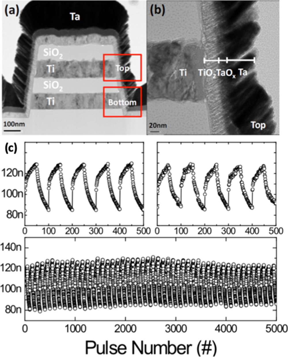
An efficient and accurate training can be obtained by adjusting the weight correction Δwij to be linearly dependent on the product of x and δ, as expressed in equation (2). For this purpose, a high degree of linearity is requested to the weight updates of the memory devices. Such highly linear update of the memory conductance can in principle be obtained with any analogue resistive device by a closed-loop scheme, such as a program-verify algorithm to accurately update the device conductance. However, the degradation of speed performance becomes unacceptable, thus steering the programming technique towards an open-loop tuning. In the recent years, there has been a clear progress in improving the linearity of synaptic devices by means of pulse-width modulation or material stack engineering [96]. For instance, figure 6 shows an example of a vertical RRAM (a) where the switching layer consists of a stacking of TaOx and TiO2, interposed between a horizontal Ti electrode and a vertical Ta top electrode (b) [96]. This type of vertical RRAM is particularly promising in view of the superior scaling with respect to the horizontal stacking of horizontal crosspoint arrays [97]. Figure 6(c) shows the corresponding weight update characteristics under open-loop application of pulses with a fixed voltage, indicating that a proper engineering of the RRAM stack enables good linearity and high repeatability of analogue update [98].

Figure 6. Vertical RRAM synapse. (a) Structure of the vertical array, where each cell is interposed between stacked horizontal Ti electrodes and vertical Ta electrodes deposited on the sidewall of a trench. (b) RRAM structure, including a TaOx/TiO2 stack as switching layer. (c) Characteristics of pulsed potentiation and depression, indicating repeatable conductance window of about 35% with gradual switching. Adapted with permission from [96, 98]. Copyright 2013 IEEE, Copyright 2016 IOP Publishing Ltd.
Download figure:
Standard image High-resolution imageFigure 7(a) shows the weight update characteristics for the TaOx/TiO2 bilayer stack of figure 6, where the depression characteristic is shown with reversed pulse count [96, 99]. The weight update characteristics are compared with other synaptic RRAM devices, namely (b)PCMO [95, 100], and (c) amorphous Si with an Ag top electrode [101]. Pulses with equal voltage were applied during both potentiation and depression. In general, RRAM synapses show some degree of nonlinearity in both potentiation and depression, which might result in inaccuracy for image and speech recognition [95].

Figure 7. Synaptic weight update characteristics for (a) TaOx/TiO2, (b) PCMO, and (c) Ag:a-Si synapses, indicating various degree of linearity, symmetry and window of the conductance change. Pulses of fixed positive/negative voltage were applied during potentiation and depression, respectively. Adapted with permission from [99]. Copyright 2015 IEEE.
Download figure:
Standard image High-resolution imageThe synaptic linearity can be improved by increasing the complexity of the synaptic structure. For instance, it has been shown that a one-transistor/2-resistor (1T2R) structure can improve the update linearity, despite the increased synapse area because of the additional transistor and resistance [102]. Alternatively, the update linearity is generally improved in synaptic transistors as in figure 3(b). These 3-terminal structures such as Li-based ECRAM devices [73, 80] or organic-based memories [79], can achieve a high linearity of potentiation/depression, despite a relatively small window of conductance. Figure 8(a) shows the update characteristics for a Li-based ECRAM device, indicating an almost linear behavior for both potentiation and depression across a relative window by a factor 3 [80]. From figure 8(a), a linearity factor can be defined as the coefficient ν in the potentiation formula G = Gmin + G0(1−e−νp), where Gmin is the minimum conductance, G0 is a reference conductance describing the synaptic window, and p is the normalized number of pulses [80, 103]. Figure 8(b) summarizes the linearity factor ν for various synaptic stacks, including PCMO [95, 100], TaOx/TiO2 RRAM [96], Ag/a-Si RRAM [101], AlOx/HfO2 RRAM [104] and capacitor-based structures [105]. PCM synapses are also included in the comparison, although they can provide weight update in one direction only, namely potentiation by gradual crystallization of the phase change material [21]. Among all materials reported in figure 8(b), ECRAM combines excellent linearity and symmetry of the potentiation/depression update. In addition, the update and read paths can be separated in the device, corresponding to the gate-channel and the source-drain terminals, respectively, thus enabling a good reliability and low energy operation. This is supported by figure 8(c), showing the energy per spike for weight update as a function of the synapse conductance, which describes the energy during the feedforward operation of the neural network. The figure compares various synaptic technologies including ECRAM [80], AlOx/HfO2 RRAM [104], TaOx/HfAlyOx RRAM [106], PCMO [107], HfOx/TiOx [108], HfO2 [109], and PCM [110]. ECRAM devices show a low conductance, enabling low current operation of the neural network in the inference mode, combined with a low energy per spike during weight update, thus offering a promising solution as a synaptic technology with high energy efficiency.

Figure 8. Characteristics of the ECRAM synaptic device. (a) The update characteristics indicate low nonlinearity with low coefficient ν. (b) Summary of nonlinearity coefficients comparing ECRAM with various RRAM and PCM. (c) Summary of the energy per spike during potentiation/depression, as a function of the device conductance, the latter providing a metric for the energy consumption during spike transmission. Adapted with permission from [80]. Copyright 2018 IEEE.
Download figure:
Standard image High-resolution imageIn addition to linearity, symmetry and energy efficiency, other key concerns for synaptic implementations are the granularity of conductance steps and the associated variability. To increase the available number of steps and reduce the stochastic variability, a novel weight structure combining multiple PCM devices in parallel was proposed [110]. The overall weight is obtained by the summation of all the parallel conductances. During training, the weight is updated by programming only one device each time. This implementation increases the overall dynamic range of the weight, since the maximum and minimum achievable weights are now N times larger, where N is the number of parallel memory devices in the synapse. The single conductance step is instead determined by a single device, thus reducing the impact of device variability [110].
Figure 9(a) shows an advanced weight structure consisting of a differential pair of PCM devices, with conductances G+ and G−, and a third conductance g of a capacitance-controlled transistor. These synaptic conductances have different significance within the overall synaptic weight W, which is given by the formula [111, 112]:

where F is a gain factor for the multiplication of the PCM weight. As a result, the PCM devices are used as the most significant pair (MSP), which is amplified by the gain factor F = 3, which thus increases the maximum and minimum implementable weights. The least significant pair (LSP) is instead given by g–gshared, where gshared is a reference conductance shared by all the synaptic elements on the same row. The LSP is implemented by using 3-transistor/1-capacitor (3T1C) CMOS structures. The weight update during training is performed on the LSP by increasing or decreasing the amount of charge on the capacitor. The latter capacitor drives the gate of a MOS transistor, which results in a tunable source conductance. The capacitor is charged by a p-MOS and discharged by an n-MOS, thus the conductance updates have similar amplitudes in either potentiation or depression. This enables the sharing of the reference 3T1C structure with conductance gshared among many weights, thus resulting in a high integration density [111]. Once every thousands of training epochs, the total weight W composed by the MSP and LSP is read and transferred into the PCM MSP, thus preserving the non-volatility of the overall weight. The LSP is then reset, enabling further training without the risk of capacitor saturation. Since the transfer operation is not frequent, the PCM devices can be programmed using a closed-loop procedure which ensures accurate weight programming [111]. The reduced number of PCM programming steps also allows to minimize any possible degradation due to potentiation/depression cycles.

Figure 9. Advanced synaptic structure to improve linearity. (a) The synaptic weight is implemented using two resistive devices, such as PCMs, and a 3-transistor/1-capacitor (3T1C) structure. The conductance g of the 3T1C structure represents the LSB, which is regularly updated, whereas the PCM represents the MSB, which is updated only once every thousand cycles. (b) A sample of the MNIST dataset for training and testing the accuracy of the neural network. (c) Accuracy for learning the MNIST dataset, indicating that testing results are equivalent to TensorFlow results. Adapted with permission from [111]. Copyright 2018 Springer Nature.
Download figure:
Standard image High-resolution imageThe weight structure in figure 9(a) allows to execute supervised training with conventional small and medium-size datasets such as MNIST (figure 9(b)), MNIST with noise, and CIFAR-10/100, and achieve software-equivalent training accuracy (figure 9(c)) [111]. A similar structure with multiple conductances of varying significance can be implemented with any pairs of nonvolatile memories, thus allowing to replace the relatively bulky 3T1C circuits. The introduction of different pairs of conductances diversifies the requests on resistive devices in LSP or MSP. For example, while high linearity and endurance are required for LSP devices, weak retention is acceptable since the transfer operation preserves the overall weight value. On the other hand, devices in MSP should show a good retention, while linearity is not necessary, due to the closed-loop programming procedure [111, 113].
5. Artificial synapses in SNNs
Most practical applications of neural networks have a typical ANN structure as shown in figure 4 and adopt a supervised technique for training the network on a specific dataset. However, this type of neural network is not similar to the brain, where learning does not take place with a supervised process such as the backpropagation algorithm. Brain-inspired learning typically occurs by unsupervised or semi-supervised processes, such as the spike-timing dependent plasticity (STDP) [29, 30, 114–118] or spike-rate dependent plasticity (SRDP) [119–122]. In these processes, the simultaneous spiking activity at two neurons can lead to a potentiation of the synapse connecting them. This can be referred to as a generalized Hebb's learning rule, where 'neurons that fire together wire together', meaning that two neurons which are active in response to the same event should be linked by a relatively strong synaptic connection [123, 124]. A similar concept is the associative memory, where the simultaneous spiking of two neurons within a recurrent neural network is awarded by synaptic potentiation to strengthen their respective synaptic links. Note that Hebbian and STDP rules are dictated by time, which is an essential variable describing the information within a SNN, as opposed to the synchronous timing in an ANN.
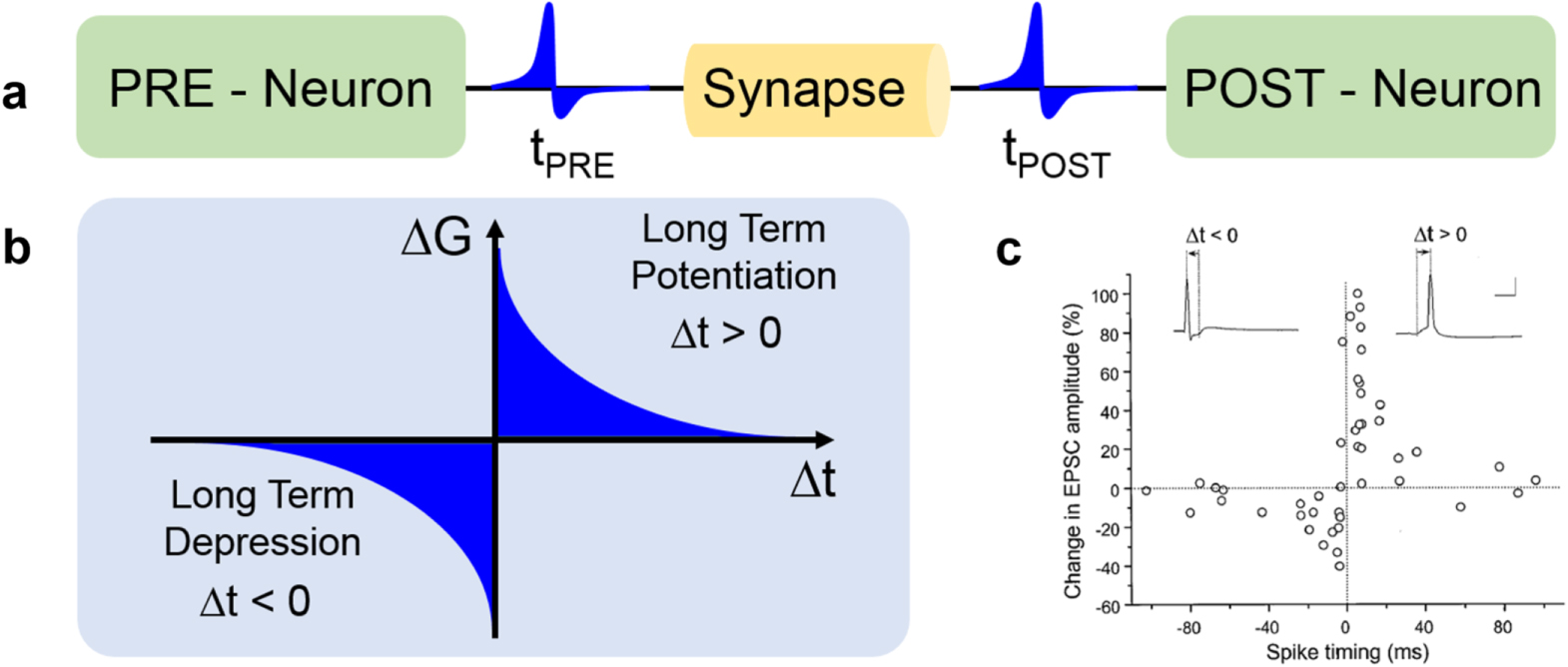
Figure 10(a) illustrates the STDP learning rule, where the synaptic weight of a synapse is dictated by the relationship between the PRE spike time tPRE and the POST spike time tPOST. In particular, if the POST fires after some time Δt = tPOST − tPRE > 0 from the PRE spike, then the synaptic weight increases, while if Δt is negative, i.e. the PRE spike follows the POST spike, then the synaptic weight decreases. This is summarized in figure 10(b), showing the change of synaptic conductance as a function of Δt: long-term potentiation (LTP) with an increase of conductance occurs for Δt > 0, whereas long-term depression (LTD) is seen for Δt < 0. For relatively long delays Δt, no synaptic change is observed. Figure 10(c) shows experimental characteristics of STDP from the hippocampus, supporting the relevance of STDP as a learning rule in biological neural networks [29].

Figure 10. Spike-timing dependent plasticity (STDP) rule. (a) STDP controls the weight update within a synapse based on the timing between the spikes of the pre-synaptic neuron (PRE) and the post-synaptic neuron (POST). (b) Typical STDP characteristic, where the conductance variation ΔG is positive (long-term potentiation) for positive delay (POST spike following the PRE spike), and it is negative (long-term depression) for negative delay (PRE spike following the POST spike). (c) Data from in vivo biological samples from the hippocampus provide direct confirmation of the STDP. Adapted with permission from [29]. Copyright 1998 Journal of Neuroscience.
Download figure:
Standard image High-resolution image5.1. Overlap STDP
There have been extensive efforts to implement STDP in hardware synapses adopting emerging memories. A synchronous protocol for STDP was proposed according to a time-division multiplexing (TDM) of neuronal signals passing through a synapse, the latter consisting of a bipolar switching resistive memory such as a RRAM [125]. The proposed scheme allows to separate the two major roles of the synapse, namely (i) transmission of neuron spikes with proper weight, and (ii) learning or plasticity, where the weight is adjusted in response to the timing of PRE and POST spikes. The adjustment occurred via overlap of pulses for either LTP or LTD using pulse width modulation (PWM) of spiking signals. For instance, overlapping pulses at the two terminals of the RRAM device can result in a positive voltage drop across the memory device exceeding the threshold for set transition, thus leading to LTP. A similar concept was later introduced to implement STDP in real RRAM devices with Ag as top electrode and amorphous Si as switching layer [101]. In this type of devices, which are generally referred to as conductive-bridge random access memory (CBRAM), the CF originated from migrating cations from the top electrode, such as Ag [126–130] or Cu [131–134].
Figure 11 shows a more straightforward approach to STDP implemented in a RRAM device with HfO2 switching layer [135]. Here, the shape of the neuron spikes is tailored to achieve a certain STDP response by overlap of pulses [13]. For instance, figure 11(a) shows that each spike consists of a train of 6 pulses, the first being negative, while the following 5 have decreasing positive amplitudes. Ideally, none of the pulses within each spike alone can result in a change of conductance, as the threshold voltage for set and reset transitions in the RRAM are larger than the spike amplitude. However, the application of 2 partially-overlapping spikes at the 2 terminals of the RRAM device results in a possible overlap exceeding the threshold for set and reset transitions. For instance, a large positive voltage arises from the spike overlap for Δt > 0, thus resulting in a set transition and consequent LTP. On the other hand, a large negative voltage exceeding the reset threshold occurs for Δt < 0, thus leading to a reset transition, or LTD. Figure 11(b) shows the measured conductance change ΔG for a HfO2 RRAM device, indicating LTP and LTD for positive and negative spike delay, respectively [135]. This type of overlap-based STDP has been applied to several device concepts, including metal-oxide RRAM [136, 137], PCM [92, 138, 139], STT-MRAM [140], FeRAM [141], and also Flash memories with a floating gate [142, 143] or a nanocrystal storage layer [144]. Both multiple pulse trains and single pulses were assumed for the spike in the STDP [118]. The pulse shape can be adapted to achieve the desired STDP function, where LTP and LTD are obtained for a certain range of Δt [13].

Figure 11. Scheme for an overlap STDP with a RRAM synapse. (a) Trains of spikes generated by the PRE and the POST result in a potential difference across the synapse with a large positive pulse for Δt > 0, or a large negative pulse for Δt < 0. (b) Measured conductance change as a function of the spike delay Δt, indicating potentiation for Δt > 0, and depression for Δt < 0. Adapted with permission from [135]. Copyright 2011 IEEE.
Download figure:
Standard image High-resolution imageDespite the overlap STDP scheme of figure 11 can be applied to a wide variety of synaptic devices capturing various pulse shapes and STDP characteristics, the 2-terminal device structure in the figure might have some drawbacks for RRAM synapses. For instance, typical filamentary switching requires a current limitation during set, which is typically achieved by adding a series transistor in a 1T1R structure [145]. The voltage-driven set transition responsible for synaptic potentiation might thus cause uncontrolled growth of the CF with detrimental impact on synapse reliability. To overcome the limitations of the 2-terminal resistive synapse described in figure 11, 1T1R synaptic circuits were proposed for implementing overlap STDP [93, 94, 146]. In a 1T1R structure, the larger number of terminals allows to independently control spike transmission and plasticity, while offering the capability of limiting the RRAM current during set/potentiation for improved reliability. The 1T1R array also allows for a better control of the synaptic array, thanks to the select transistor in series with the memory element, either a RRAM [94, 146] or a PCM [93].
Figure 12(a) shows a RRAM synapse with 1T1R structure [147]. The RRAM synapse has 3 terminals including (i) the transistor gate, connected to the input node of the PRE, (ii) the transistor source, connected to the input node of the POST, and (iii) the top electrode of RRAM device. The latter is connected to the POST for the control of transmission and plasticity phases of the RRAM synapse. The PRE spike of amplitude VG at the transistor gate induces a synaptic current, as the top electrode voltage VTE is normally biased to a relatively small value below the threshold for set/reset processes [146]. The synaptic current is proportional to the synaptic weight, namely the RRAM conductance, as the gate voltage is large enough to prevent any significant voltage drop across the transistor. The current flows across the transistor and enters the POST input node, which behaves as a current-summing virtual ground. The POST can thus integrate the synaptic current from several synapses, all connected to the same input node, and fires in correspondence of the internal potential reaching a given threshold [147]. At fire, the POST applies a feedback spike to the top electrodes of all synapses activating STDP process. Figure 12(b) shows the PRE spike (top) and the POST (feedback) spike (bottom) as a function of time, in the case of a small positive delay Δt between the spikes [147]. The feedback spike includes a positive pulse and a negative pulse, exceeding the threshold for set and reset transition of the RRAM device. For Δt > 0, there is an overlap between the PRE spike and the positive pulse of the POST spike, thus causing a set transition, or LTP. On the other hand, for Δt < 0, the overlap occurs at the negative top electrode voltage, which thus induces a reset transition, or LTD. Note that the transistor controls the current during set transition, thus setting a maximum limit to the RRAM conductance after LTP. On the other hand, LTD is self-limited by the highest resistance of the HRS, typically from one to two decades larger than LRS. Figure 12(c) shows the STDP characteristics, namely the conductance change η = log10(G/G0), where G is measured after the STDP event while G0 is measured before the STDP event, as a function of Δt and the initial resistance R0, which is the reciprocal of G0. The data generally indicate that the synapse is potentiated for Δt > 0 and depressed for Δt < 0, although the amount of LTP/LTD depends on the initial conductance. For instance, LTD is inhibited when the initial state is the HRS, since the conductance cannot be decreased below a certain minimum amount. Similarly, LTP is inhibited when the device is initiated in the LRS, thanks to the compliance current controlled by the transistor.

Figure 12. Scheme for an overlap STDP with a 1T1R structure. (a) Circuit scheme for the 1T1R synapse, where the PRE spike is applied to the transistor gate, while the POST spike is applied to the top electrode. The current spike is activated by the PRE spike and fed into the POST through the bottom electrode. As the integrated PRE spikes lead to fire, the POST spike is applied to the TE, thus inducing potentiation or depression depending on the spike delay Δt. (b) PRE and POST spike for Δt > 0, where the resulting overlap pulse is positive, thus inducing set transition, or potentiation. (c) Measured conductance ratio η = log10(G/G0) as a function of initial resistance R0 and spike delay Δt, indicating potentiation for Δt > 0, and depression for Δt < 0. Adapted from [147].
Download figure:
Standard image High-resolution imageThe 1T1R synapse can be generalized to other memory elements by changing the feedback spike shown in figure 12(b). For instance, the feedback spike includes 2 positive pulses in the 1T1R PCM synapse, the first being a relatively small set pulse below the melting voltage, whereas the second is above the melting voltage to induce a reset process [93]. A possible limitation of the STDP characteristics in figure 12(c) is the rectangular shape, instead of the exponential dependence on Δt [13]. For an improved control of the STDP characteristics, the two-transistor/1-resistor (2T1R) structure was proposed for RRAM [148] or PCM [149]. In the 2T1R synapse, the two gates activate the memory element for either transmission or plasticity, while the top electrode node is connected to the PRE. Applying a time-dependent gate voltage at the plasticity transistor from the POST, one can freely change the set transition current at the device, thus shaping the time dependence of the LTP. The time dependence of the LTD can be instead dictated by the top electrode voltage from the POST [148]. The 1T1R synapse of figure 12 was also adapted to SRDP, with the addition of few transistors resulting in a four-transistor/one-resistor (4T1R) structure [150, 151].
The STDP rule is an enabling algorithm for unsupervised learning of patterns in space [93, 146, 147, 150, 152–157] and space/time [158]. Figure 13(a) shows a prototypical neural network, namely a one-layer perceptron with 16 PREs and one POST, to test the ability to learn via STDP [147]. This network was implemented in hardware by using RRAM synapses with 1T1R structure, as the one described in figure 12. PRE spiking signals were applied to the transistor gate electrodes, while all synaptic currents were summed in real time and integrated by a microcontroller Arduino due serving as the POST. At fire, POST feedback spikes were applied to all the synaptic array, thus resulting in LTP and LTD, depending on the relative delay between PRE and POST spikes according to STDP rule. Figure 13(b) shows the applied spikes, consisting of a space 4 × 4 pattern which was changed in time during three sequential phases of training of the network. Unsupervised learning is inherently stochastic, meaning that noise patterns must also be submitted randomly to the network to induce LTD as a result of uncorrelated PRE noise spikes following the POST fire. Figure 13(c) shows the synaptic conductance before the training session, and after each of the three training phases, always indicating the correct learning of the input pattern with no remaining traces of the previous pattern. The ability to 'forget' the pattern from the previous phases can be attributed to the LTD at the background positions within submitted pattern, where only random noise is presented, thus inducing LTD [147]. Figure 13(d) summarizes the submitted spikes, including both pattern and noise spikes, and figure 13(e) shows the time evolution of all the measured synaptic weights. The ability for unsupervised learning can be extended to larger networks, e.g. to enable learning of realistic input patterns such as the handwritten digit images from the MNIST dataset [93, 159, 160]. The STDP rule in 1T1R synaptic RRAM was also shown to support spatio-temporal learning [158] and associative memory behavior within a Hopfield recurrent neural network [161].

Figure 13. Unsupervised learning in a one-layer perceptron with RRAM synapses. (a) Illustration of the one-layer perceptron, where a pattern is presented at the input neuron layer (PRE) via spikes, while the single POST integrates the spiking currents across each synapse. (b) Examples of 4 × 4 visual patterns and typical noise presented at the PRE layer. (c) Initial and final synaptic weights after sequential presentation of three patterns. (d) Summary of the presented patterns during three sequential phases. (e) Time evolution of the synaptic weights for pattern synapses, i.e. those belonging to the pattern, and background synapses, i.e. those not belonging to the pattern. Pattern and background synapses display potentiation and depression thanks to unsupervised learning. Adapted from [147].
Download figure:
Standard image High-resolution image5.2. Non-overlap STDP
The STDP learning rule by overlapping spikes is generally robust and reliable, however it also has drawbacks in terms of energy consumption and pulse-width. In fact, the PRE spike pulse-width must be at least the same as the scale of delay time of the STDP characteristics in figure 12(c), because there is no memory effect taking place in the RRAM element after the end of the PRE spike. The long spike pulse-width results in a large energy consumption during the spike, as well as an excessive occupation of interconnect lines in address-event-representation architectures which are typical for multicore SNNs [162].
To overcome the limitations of the overlap learning scheme and enable the development of non-overlap neuromorphic devices, the inherent memory properties of emerging memories can be considered. Figure 14(a) shows a schematic of an atom-switch RRAM, consisting of a stack of a metal top electrode, an Ag bottom electrode, and an Ag2S film as solid-state electrolyte [163]. Differently from the CBRAM device, a vacuum nanogap is interposed between the top electrode and the solid electrolyte. The application of voltage pulses to the top electrode can lead to the formation of an Ag atomic bridge across the nanogap [164]. In addition, figure 14(a) evidences that the atomic switch can act as an artificial synapse since repeated pulses can lead to the gradual formation of an atomic bridge, according to a sequence of a first phase of short-term potentiation (STP), followed by a second phase of LTP [163]. This dynamic behavior can also lead to SRDP, where STP or LTP behaviors are observed depending on the spiking frequency. In particular, the application of spikes with relatively low frequency results in STP, where the RRAM conductance increases temporarily, then decays within the period before the next spike is applied (figure 14(b)). On the other hand, the application of spikes at higher frequency induces LTP, as each spike contributes causing an additional increase in conductance reaching a maximum value of about 80 μS after just 5 spikes (figure 14(c)).
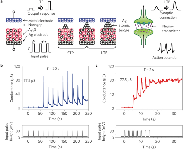
Figure 14. Scheme for a non-overlap synapse based on an atomic switch. (a) Schematic of the atomic switch consisting of a RRAM device where the applied pulses induce the migration of Ag cations within a nanogap leading to the formation of an atomic bridge. The pulse frequency dictates the transition from STP to LTP, similar to the biological synapse. (b) Measured conductance (top) in response to a low-frequency stimulation (bottom) indicating STP with fast decay after each pulse. (c) Measured conductance (top) in response to a high-frequency stimulation (bottom) indicating LTP reaching permanent increase in conductance. Reprinted with permission from [163]. Copyright 2011 Springer Nature.
Download figure:
Standard image High-resolution imageSimilar dynamic effects have been reported in RRAM devices. Figure 15(a) schematically illustrates the concept of second-order memristor, namely a RRAM synapse which can learn depending not only on the pulse amplitude, but also on the time delay between two successive spikes [165]. As illustrated in figure 15(b), if the time delay Δt between two pulses with relatively low amplitude is long, no conductance change is observed, whereas the conductance increases if the second pulse is applied at short time delay from the first one. This second-order dynamic behavior has been explained by the role of the local temperature within the device: when the second pulse is applied at short delay after the first one, the device local temperature is still relatively high, due to the limited thermal time constant which was estimated around 500 ns [165]. The high local temperature thus assists the ionic migration at the origin of the conductance change, which could lead to non-overlap STDP and SRDP processes in a Pd/Ta2O5−x/TaOy/Pd RRAM synapse [165].

Figure 15. Non-overlap synapse based on a second-order memristor. (a) Schematic of the second-order memristor where the application of a first stimulus causes a temporary increase in conductance, followed by a spontaneous decay. The application of a subsequent stimulus can induce a permanent conductance change. (b) Illustration of the second-order memristor dynamics, where the application of a sequence of two spikes can lead to synaptic potentiation only if the spike delay Δt is sufficiently short, otherwise no conductance change takes place. Adapted with permission from [165]. Copyright 2015 American Chemical Society.
Download figure:
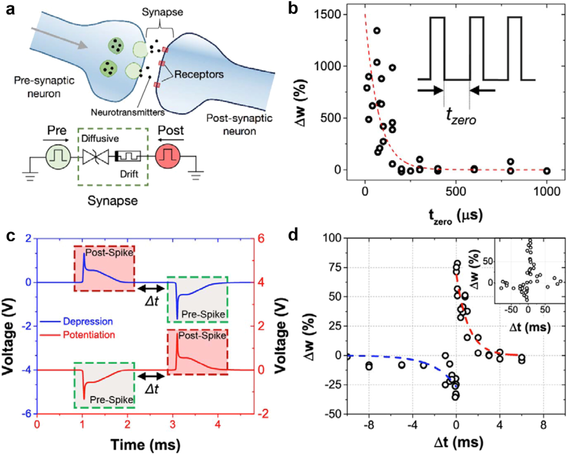
Standard image High-resolution imageFigure 16(a) shows a similar concept for a non-overlap synapse based on a one-selector/one-resistor (1S1R) structure, where the resistor device is a nonvolatile RRAM, while the selector device is a volatile RRAM [166]. The volatile RRAM, also referred to as diffusive memristor, consists of a stack of Ag top electrode and an oxide solid electrolyte, such as SiOxNy [166], SiOx [167] and HfOx [168]. In these devices, similar to the atomic switch in figure 14, the CF formed by the application of a positive voltage pulse to the top electrode spontaneously disconnects after a characteristic retention time in a variable timescale from few ns [168] to the μs or ms range [169]. This volatile behavior has been explained in terms of the impact of the mechanical stress surrounding the CF [130] and the surface tension aiming at minimizing the surface-to-volume ratio of the metallic filament [166, 170].

Figure 16. Non-overlap synapse based on volatile RRAM, also called diffusive memristor. (a) Schematic of the 1S1R synapse, consisting of a volatile RRAM (1S) and a nonvolatile RRAM (1R), where PRE and POST spikes are applied, similar to a biological synapse with neurotransmitters and receptors. (b) Conductance change Δw as a function of the spike delay for a train of spikes. Potentiation decreases with increasing delay between spikes, thus mimicking the SRDP of biological synapses. (c) Illustration of the sequence of POST spike followed by PRE spike (top), or the sequence of PRE spike followed by POST spike (bottom), with a delay Δt between the spikes. (d) Conductance change as a function of the delay between PRE and POST spikes, showing STDP dynamics similar to the biological synapse. Reprinted with permission from [166]. Copyright 2016 Springer Nature.
Download figure:
Standard image High-resolution imageThe combination of volatile and nonvolatile RRAM devices in the synapse of figure 16(a) enables SRDP as summarized by the weight change Δw as a function of time separation between spikes tzero in figure 16(b). The dependence on spiking frequency can be explained by the competition between synaptic potentiation induced by the electric field during the spike, and synaptic relaxation induced by surface diffusion during the waiting time tzero [171]. Similarly, a non-overlap concept for STDP was demonstrated, as summarized in figures 16(c) and (d) [166]. These and other artificial synapses based on the rich physics of emerging memory devices might spur the development of novel neuromorphic systems which can parallel the energy efficiency and parallelism of the human brain.
6. Neuron circuits
The synapse is generally assumed to serve as passive element to store the weight, while the neuron plays the role of active element executing current summation, integration and threshold firing. Due to the large area occupation and power consumption that CMOS circuits require for neuron implementation, it is desirable to follow a different approach where portions of neuron functionalities could be realized with compact and low-power resistive devices. As an example, the integration of spikes in a spike-based network, which is typically performed with large capacitors receiving current contributions, has been recently demonstrated via emerging memory devices [172]. A similar type of accumulating neuron has been proposed by using RRAM devices based on PCMO [173] and Ag/SiOxNy stack [174].
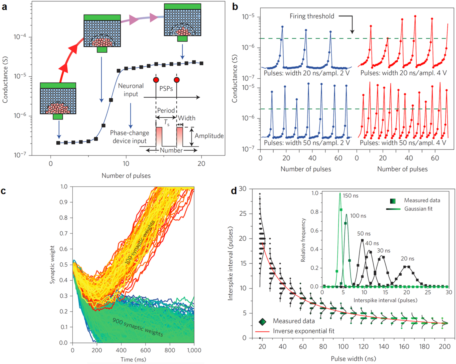
Figure 17 shows a possible implementation of an integrating neuron using a PCM device [172]. While conventional CMOS integrators rely on capacitive elements to accumulate charge induced by voltage or current spikes, this type of memory-based neuron integrates the voltage spikes by inducing a partial crystallization within the amorphous volume, as shown in figure 17(a). Here, each voltage pulse leads to a local Joule heating within the memory device, thus resulting in an increasing crystallization by nucleation and/or growth of the crystalline phase. Since the crystalline phase has a lower resistivity than the amorphous phase, the PCM conductance increases at each step, thus serving as the internal membrane potential of the biological neuron. When the conductance reaches a threshold, a fire event is triggered, corresponding to an output voltage spike generated by the neuron circuit. In addition, the PCM device is reset back to the amorphous phase, as shown in figure 17(b), thus allowing to operate the spike integration in the next cycle. The modulation of the voltage pulse in terms of voltage amplitude and pulse-width leads then to different and controllable firing rates.

Figure 17. Phase change neuron. (a) PCM conductance as a function of the number of applied spikes, indicating a gradual increase due to the growth of the crystalline phase within the active region of the phase change material. (b) Conductance change as a function of the number of spikes, or various pulse width (top: 20 ns, bottom: 50 ns) and amplitude (left: 2 V, right: 4 V). The conductance increases until it exceeds a certain threshold, then the low conductance is restored by a reset operation. (c) Synaptic weight for two distinct sets of PCMs, corresponding to active synapses where the applied spikes induce potentiation, or inactive spikes leading to depression. (d) Number of spikes to reach the threshold as a function of the pulse width. Adapted with permission from [172]. Copyright 2016 Springer Nature.
Download figure:
Standard image High-resolution imageNote that the PCM device is only suitable for integration, while an additional CMOS circuit is needed to provide the spike generation and the optional refractory period. Based on this concept, the authors demonstrated a single layer perceptron specialization with STDP algorithm and one PCM neuron. This is illustrated in figure 17(c), showing the conductance of two distinct families of synapses, corresponding to synapses being active within the pattern, thus receiving potentiation, and synapses being non-active because not involved in the pattern channels, thus receiving depression [172]. Another crucial feature for brain-inspired artificial neurons is the intrinsic stochasticity of integration and fire. To this purpose, the PCM firing pulses were shown to feature a natural stochastic behavior, as every reset operation results in a statistically different atomic structure within the amorphous phase, thus causing variable conductance paths and crystallization times during integration, hence random neuron fire events. Figure 17(d) reports the distribution of times between successive fire events as a function of the input voltage pulse-width, which supports the ability to control the amount of stochasticity by changing the programming conditions [172].
Many learning schemes in SNNs, such as STDP, require neurons with leaky integrate-and-fire functionality, to elaborate the incoming spike and provide signals to the next neuron layers. Other computing schemes instead rely on neurons emitting a train of spikes with controllable rate. According to the neuron model of Hodgkin and Huxley [175], the cell membrane releases an action potential with a specific shape and a refractory period. Volatile memory devices enable the implementation of such neuron by their switching and recovery processes [176]. Figure 18(a) shows an example of neuron circuit implemented with a couple of RRAM devices based on NbO2, described by the I–V curves in figure 18(b) [176]. NbO2-based RRAM devices are characterized by a typical threshold switching behavior, where the device shows a transition from the off-state to the on-state, followed by a transition back to the off-state [177–179]. Combining one or more threshold switches with a parallel capacitor as in the circuit of figure 18(a) thus results in controlled relaxation oscillations which can be adopted to generate spike trains with various shapes. The neuron circuit of figure 18(a) is in fact able to generate a time-oscillating dynamics thanks to a constant input current. Figure 18(c) provides a comparison of experimental and simulated results, where a neuron biased at a constant current I = 20 μA delivers spike trains with tunable inter-spike intervals depending on the capacitance values C1 and C2 [176].

Figure 18. Mott insulator neuron. (a) Schematic of the neuron circuit including two coupled relaxation oscillators based on NbOx RRAM. (b) I–V characteristics of the NbOx RRAM with crosspoint structure (inset). The curve indicates threshold switching from the off-state to the on-state, followed by a return back to the off-state at the characteristic holding voltage of about 1.3 V. (c) Oscillating dynamics of the neuron. As the DC bias voltage increases, the fire rate increases as a result of the relaxation oscillator dynamics. Adapted with permission from [176]. Copyright 2013 Springer Nature.
Download figure:
Standard image High-resolution imageAlthough the NbOx-based oscillating neuron shows excellent agreement with biological neurons, the need for integrated capacitors prevents easy scalability toward very high density. For this reason, achieving a neuron with oscillating functionalities inherently in a single device is desirable. Figure 19(a) shows an example of a single nanodevice oscillator [180]. The device structure consists of two FM layers separated by a non-ferromagnetic material, such as a MgO tunneling barrier. The applied current flows across the bottom layer which shows a fixed in-plane magnetization. The bottom layer causes the spin-polarization of the flowing electrons, which eventually cause the rotation of the magnetic polarization of the top FM layer. The rotation of the magnetization leads to a variation in the device electrical resistance due to the tunneling magneto-resistance (TMR) effect [62], with a consequent oscillation of the voltage drop across the device, as shown in figure 19(b). Figure 19(c) shows the amplitude of the voltage oscillations as a function of the bias current, indicating that the oscillation amplitude increases with the applied current [180]. This nanomagnet oscillator thus provides a remarkable scheme for controllable spiking neurons with extremely small area and high density.

Figure 19. Magneto-resistive neuron. (a) Schematic of a superparamagnetic junction, where a bias current IDC induces an oscillating dynamics due to magnetic precession. (b) Oscillating output voltage as a result of the resistance change due to the MTJ effect. (c) Amplitude of the voltage oscillation as a function of IDC. (d) Neuron circuit combining a DC bias and an external stimulation. (e) Typical input/output voltage, where a constant voltage input results in an oscillating output voltage with variable amplitude. Reprinted with permission from [180]. Copyright 2017 Springer Nature.
Download figure:
Standard image High-resolution image
Based on this principle, the input information can be sent to the oscillator by superposing a signal VIN to a constant current IDC. The input signal thus causes a modulation of the oscillation amplitude, as shown in figures 19(d) and (e). Interestingly, the envelope curve  (t) in figure 19(e) shows a relaxation time on the scale of tenths of nanoseconds providing a memory effect which can be used to perform computation [180]. In fact, the state of downstream neurons in a trained neural network depends on the state of neurons in the previous layer. Similarly, the same concept can be translated in time, where the state of a neuron in the future depends on the state of the same neuron in the past [180]. Based on this concept, a neural network adopting a single oscillating nanomagnet neuron allows to recognize audio waveforms of single spoken digits pronounced by five female speakers [180]. A similar concept of oscillating nanodevice was proposed by harnessing random telegraph signal within a single RRAM device [181]. These results support memory devices as a very promising approach for small-area neuron circuits, where computation takes place via the inherent device physics.
7. Comparison of device technologies for neuromorphic computing
Several devices based on radically different physical concepts have been previously presented, which provides a variety of useful features for neuromorphic computing. Table 1 shows a summary of the various device concepts, comparing RRAM, PCM, MRAM, FeRAM and Li-ion devices in terms of performance, reliability (drift, endurance, retention), and most importantly their ability to fulfill the requirements for neuromorphic computing, such as the linearity for weight update, the density of the synaptic array, and their energy consumption. Based on these properties, each device shows a different suitability for DNNs and SNNs, which is discussed in the table.
Table 1. Summary and comparison of neuromorphic device technologies in terms of performance, reliability, and their suitability for DNN training, DNN inference, and SNNs.
| RRAM | PCM | MRAM | FeRAM | Li-ion | |
|---|---|---|---|---|---|
| ON/OFF Ratio | 20–50 | 102–104 | 1.5–2 | 102–103 | 40–103 |
| Endurance | 105–108 | 106–109 | > 1012 | 1010 | >105 |
| Retention | Medium | Large | Medium | Large | — |
| Drift | Weak | Yes | No | No | No |
| Linearity | Low | Low | None | None | High |
| Integration density | High | High | High | Low | Low |
| Energy efficiency | 0.1–1 pJ/bit | 10 pJ/bit | 100 fJ/bit | 100 fJ/bit | 100 fJ/bit |
| Switching speed | <10 ns | 10–100 ns | <10 ns | 30 ns | <10 ns |
| Suitability for DNN training | No | No | No | No | Yes |
| Suitability for DNN inference | Moderate | Yes | No | No | Yes |
| Suitability for SNN algorithms | Yes | Yes | Moderate | Yes | Moderate |
While all the proposed devices generally show a promising behavior in terms of speed and energy efficiency, their large-scale integration in real hardware neural networks still represents a challenge. In particular, a clear distinction between hardware for DNN training, DNN inference and SNNs must be made. For DNN training, the logic surrounding the synaptic memory core needs to efficiently implement forward propagation, backpropagation and weight update. As a result, a DNN with on-line training capability should adopt chip architectures that enable high throughput, i.e. a large number of trained images per second, combined with a reduced power consumption to enable the implementation in embedded systems. Training also requires a high linearity of weight update, which typically represents an issue due to the nonlinear switching characteristics of memory devices. In this framework, Li-ion devices have demonstrated a relatively high degree of linearity, although this technology is not yet mature enough and high integration density has not yet been achieved. While using a pair of devices to implement a synaptic weight leads to extremely high requirements of linearity [182], more complex structures involving multiple pairs of devices for each weight can reduce that requirement [113]. Although this novel architecture has lower integration density, it may improve the opportunities of nonlinear synaptic devices such as RRAM and PCM for DNN training circuits.
Hardware for DNN inference should be characterized by an extremely low latency, namely a short time for the classification of the original input, combined with low power operation to enable embedded systems in smartphones, cars, smart sensors, and so on. In this case, the logic circuit controlling the synaptic memory core is relatively simple, as no backpropagation and weight update schemes are involved. On the other hand, the memory should display a high retention of analogue states, also in terms of conductance drift and noise which result in a slow degradation of the stored weight. Linearity is no longer a strict requirement, since training is executed off-line and the programming operation can be performed just once with a write-and-verify technique [113]. Here, RRAM and PCM provide the most promising results thanks to the analogue conductance tuning enabling weight encoding. From this standpoint, high-density 3D crosspoint architectures where multiple memory arrays are stacked thanks to back-end select diodes seem the most promising technology [17, 18, 183, 184].
SNNs may find their application in sensors or embedded systems, thus requiring low-power consumption. In such cases, extremely high accuracy and speed are not strictly required, since real-world sensors usually just provide an initial image or video pre-processing and do not update information faster than 100 or 1000 times per second. Energy consumption should be as low as possible to preserve the functionality for long times even in battery-operated systems. In addition to that, spiking neurons and synapses should display a relatively high endurance, since spiking algorithms typically rely on a continuous learning procedure, and stochastic neurons need for continuous reset after each integrate and fire cycle. A high resistance window ensures a suitable ratio between the weights of potentiated and depressed synapses, which is beneficial for continual learning [185]. Analogue weight storage might not be essential for implementation of SNNs, which opens opportunities to adopt devices with relatively narrow memory window, such as STT-MRAM.
Finally, a major challenge for all these hardware implementations consists of the flexibility and reconfigurability of the network. Today, the advancement of software algorithms and network topologies is extremely fast, with new architectures generated every year. To become industrially relevant, neuromorphic chips based on resistive devices should be able to account for network reconfigurability, providing as many design degrees of freedom as conventional CPUs and GPUs [186].
8. Conclusions and outlook
Neuromorphic circuits are gaining momentum as an alternative computing paradigm complementing the conventional digital circuits at the end of Moore's law. By taking inspiration from the architecture and processing scheme in the brain, the neuromorphic circuits offer the possibility to perform advanced tasks, such as recognizing objects in an image frame, or translating a speech to a different language. In carrying out such important tasks, however, it is essential that the minimum energy is consumed in the least computing time within the smallest possible circuit.
In this scenario, memory devices show a very attractive wealth of physical processes, combined with an extreme scalability thanks to material switching, which makes this class of devices the most promising technology for future neuromorphic circuits.
Despite the very strong opportunities of memory devices in neuromorphic computing, there are indeed several steps to be taken to fully support a memory-centric neuromorphic technology. First, it clearly appears that DNNs and SNNs rely on different computing concepts, thus the synapse/neuron devices should have correspondingly different properties. For instance, it appears that analogue or multilevel switching is essential for DNN synapses, whereas SNNs might rely on stochastic, binary synapses. Also, SNNs make large use of integrate-and-fire neurons, whereas a nonlinear amplifier is needed as neuronal element in DNNs. In addition, artificial synapses and neurons are usually implemented with various type of nanodevices, e.g. a nanomagnetic spiking neuron and a hybrid CMOS/RRAM synapse. Finally, 3D integration technology might be needed to achieve the necessary neuron/synapse density to reproduce a brain-like cognitive function. As a result, a full neuromorphic hardware might result in a complicated system combining various types of devices with 3D process integration.
The stochastic variation and lack of repeatability might still be an issue toward the development of DNNs, where the recognition accuracy is subject to a careful, extensive training of the synaptic weights. Reliability issues such as the resistance drift in PCM [187] or the stochastic fluctuation of resistive states in RRAM [188] might represent serious threats toward achieving a high recognition accuracy matching the software implementations of the neural network. A solution to these issues might require careful engineering of the device from the materials, geometry, and algorithm points of view, which are all subject to a better understanding of the switching mechanisms and the associated reliability issues. A deeper insight into the switching processes in the memory devices might also set the stage for improved numerical and compact models for the design of neuromorphic circuits and a better device-circuit co-design of the integrated system.
In addition to device-specific challenges, understanding the scope of neuromorphic hardware is still a general point of debate. DNNs find natural application in image and speech recognition, where the development of neuromorphic devices enabling a higher density, a faster training and a lower energy consumption will further spur the transition of AI from cloud computing to edge computing, e.g. the ability to recognize and translate a speech on a smartphone. On the other hand, the potential applications for brain-inspired SNNs are not clear yet. While unsupervised learning and spiking operation are clearly attractive features for a neuromorphic system aiming at replicating the human brain, there has not been any compelling evidence that a SNN can even barely get close to the capability of a full cognitive system. A strong barrier toward achieving a brain-like neuromorphic computer on a chip is the lack of our understanding about how information is processed within the human brain. Solving this mystery would spur the development of SNNs and drive the demand for neuromorphic devices, where memory devices might offer unprecedented advantages in terms of scaling and functionality thanks to their unique physical properties.
Acknowledgments
We acknowledge Valerio Milo for critical reading of the manuscript. This article has received funding from the European Research Council (ERC) under the European Union's Horizon 2020 research and innovation programme (grant agreement No. 648635).