

Abstract
The development of neuromorphic computing architectures based on two terminal filamentary resistance switching devices is limited in part by the high degree of variability in resistance states and switching voltages. Because of the large role filament shape plays in directing thermal and electric fields around the filament (and thus switching parameters), unambiguous knowledge of filament morphology resulting from direct characterization of filament shape is essential to solve critical ongoing challenges of device switching variability. Here, we have utilized a conductive atomic force microscopy scalpel technique to simultaneously scribe through a polycrystalline dielectric layer in formed Cu/HfO2/p+Si electrochemical metallization cell devices. Filament tomograms reveal that when conductive filaments are formed at typical bias conditions (4 V, 100 μA), a variety of filament shapes result, which deviate from the inverse conical shape predicted by the phenomenological electrochemical model. Furthermore, the observation of an increasing spectrum of damage which scales with forming voltage (associated with compliance current overshoot), and which is uncorrelated with electric field or oxide microstructure, supports the role of thermal pulses in expanding filaments, leading to irreversible dielectric breakdown structures at the extreme. Overall, these findings suggest that the original conductive filament shape can be highly varied as a result of thermally driven expansion from joule heating during the forming step, which is not explicitly accounted for in the widely accepted electrochemical model.
Export citation and abstract BibTeX RIS
1. Introduction
Despite promising performance in areas of cycle endurance [1, 2], scaling [3], and power use [4], the possible technological integration of electrochemical metallization cells in neuromorphic computing has been curtailed by high levels of variability in their electrical switching parameters between cycles and between devices [5]. Fundamentally, this variability stems from the non-uniformity in the shape, volume, and composition of the conducting filaments that determine the device's non-volatile resistance state, as well as their continuing evolution over numerous set and reset cycles. These filaments are formed as the result of high electric fields (>1 MV cm−1) which are believed to drive migration of positively charged ions from the redox active metal electrode across the dielectric layer to the inert bottom electrode, shorting the dielectric layer while current is limited at a set compliance value (Icc) [6]. As an additional complication, this process of 'arrested dielectric breakdown' exists on a continuum of field driven and thermally driven dielectric breakdown, and high thermal gradients exist due to joule heating in nm scale cross-sections within ns time-scales (i.e. near adiabatic conditions) [5–8]. In the extreme, this thermal pulse can result in irreversible broadening of the filament, hard-dielectric breakdown and thus device failure [1].
Taken together, this involvement of several driving forces and their interaction with defects both in the dielectric layer as well as the electrode materials presents a complicated practical problem to identify the major determinant of filament variability or critical interface/device layer to engineer. Practically, this has resulted in a wide variety of experimental approaches to improve device performance, including the alteration of electric field distributions by the addition of nano-crystals in the dielectric layer [9] and by engineering of electrode roughness [10]. From a modeling approach, several studies have made use of analytical solutions [11–14] or finite element modeling [15] in order to understand the complicated interplay of electrical field, thermal joule heating, redox reactions, and materials defects in determining the kinetics and variability of resistance switching. In particular, the RESET operation in which the filament is dissolved has presented large degrees of device variability and challenge to model [16–18]. For many of these models, the explicit shape of the filament, whether conical, cylindrical, or hour-glass must be assumed at some step [19]. In the framework of the widely accepted phenomenological model [20], both lateral and transverse ion migration is limited in oxides, and as ions travel from anode to cathode, the electric field concentrates around the tip of the growing filament and drives increased ion flux in that area, forming a conical shape with its base at the anode. However, a growing body of experimental work concerning direct imaging of formed filaments show that while there are several reports of the predicted cone shaped filaments [21–25], hourglasses [26], branched filaments [27], and larger more cylindrical shapes [28] have also been reported. Overall, the number of studies concerning direct imaging of filament area are relatively few when compared against the vast body of work on device level characterization. This dearth stems from the fact that basic characterization of conductive filament shape is non-trivial, principally due to the challenging nature of studying nanometer scaled conductive defects within the several layer device matrix.
In order to characterize these challenging structures, studies have relied on two of the most accessible nanoscale techniques, transmission electron microscopy (TEM) and conductive atomic force microscopy (c-AFM). Studies utilizing both in-situ TEM and TEM cross-sections following device programming have revealed that conductive filaments in electrochemical metallization systems are indeed composed of metal (although the ionization state is unknown), and the conductive area seems to be enriched in metal as the device approaches failure [1, 29]. However, in the in-situ studies, the exposure of the device area may introduce artificial electric field distributions as well as artificial defect concentrations associated with the exposed surface. Likewise, moisture has been shown to be an important element in resistive switching [30], and is by nature excluded from TEM experiments. A particularly interesting aspect of filament growth has been generated by high-resolution TEM work that shows build-up of metallic clusters nucleated within the dielectric layer [31]. The first observation of these Ag or Cu clusters, and the associated growth mode in which the filament grows from anode to cathode, opposes the theoretical frame-work of field-drive ion migration followed by electro-chemical reduction at the device cathode [29]. This work has generated some debate as to whether metal ions can in fact be reduced within the bulk of the dielectric, versus nucleating and growing a filament only once reaching the cathode [32]. Although TEM has been used to reveal previously unpredicted growth modes of conductive filaments as well as show a build-up of metal within failed filaments, only a 2D slice of the filament is generated in these experiments, and the true 3D shape remains an open question.
Instead, conductive atomic force microscopy (c-AFM) studies have proven to be especially promising by virtue of combining a high sensitivity circuit and the capability of tracking topographic features with nanometer scale resolution. These studies include work in which the top electrode of a device has been removed post programming, and a 2D scan of the surface used to reveal conductive pathways (composed of either oxygen vacancies or metal atoms) through the insulating oxide matrix [33–37]. Testing between amorphous and polycrystalline materials shows that conductive spots are preferentially localized at grain boundaries, and are indeed more readily set/reset than their larger, randomly dispersed filaments in amorphous films [35, 38]. While these studies yield compelling information, they present only a snap shot after each programming step has been executed. To gain an understanding of the evolution over operation sequence, the tip has been used as a mobile 100 nm2 electrode, to which a voltage is applied as it scans over the surface of the oxide [27, 39–42]. However, these experiments often involve artificially concentrated electric fields around the sharp AFM tip, as well as read voltages high enough to influence filament forming/rupturing and program voltages >4 V.
An especially innovative alternative applies c-AFM with a doped diamond tip used both as a scalpel and a traditional conductive AFM tip [24, 43]. This technique yields the ability to create a 3D tomogram of conductive filaments with nm scale vertical and lateral resolution. Using this technique, both inverted cones [24] and hourglass filament shapes [26] have been demonstrated. Additionally, it has been determined that reset resistance states are correlated to exceedingly narrow (<10 nm radius) tunneling gaps between the filament end and the top electrode [44]. Therefore, a full analysis of filament shape in devices formed under less artificial conditions is possible using this 3D 'scalpel' technique. As yet, this promising technique has been applied in only a small subset of dielectric films out of the vast possibilities for oxide chemistry and microstructure [45]. Moreover, because of the time consuming nature of these experiments, it is difficult to establish inter-device variability in filament shape.
In this work, the 3D scalpel technique is used to investigate conductive filament shape in three p+Si/HfO2/Cu devices based on polycrystalline HfO2 layers formed under identical electrical stress conditions. Additionally, the filament shape in thick (30 nm) and thin (10 nm) HfO2 films is obtained and shows a high degree of variability between branched, inverse conical, and conical shapes. Here, a low forming voltage/electric field attainable only in polycrystalline HfO2 films is used to reduce overshoot of the set compliance current, as forming at higher voltages demonstrates an increasing spectrum of thermal damage to both dielectric and top electrode layers. The relative impacts of forming voltage (Vform), electric field, and dielectric microstructure on thermal damage mechanisms was explored using a 2D device deconstruction experiment, and demonstrated that Vform is the principal determinant of compliance current (Icc) overshoot and therefore thermal damage area, while oxide microstructure can control damage location. Notably, electrical bias conditions were chosen as representative of the forming conditions commonly employed in device scale variability studies, and the impact of those conditions on the material integrity of the device (which may normally be hidden under thick top electrodes) is revealed. These results combined with the observed variability in shape (instead of merely volume) suggests that even in oxide systems in which ion migration is kinetically limited, thermal contributions to lateral ion diffusion as well as oxide defects may play a larger role than earlier surmised in determining conductive filament shape under the given electrical bias conditions.
2. Methods
2.1. Device fabrication
p+Si/HfO2/Cu devices were fabricated on highly doped 〈100〉 p+Si substrates purchased from NovaElectronics (0.001 Ω m). Substrates were first cleaned in a buffered oxide etch solution (5:1 HF) for 30 s before loading in a Cambridge Nanotech Fiji atomic layer deposition (ALD) chamber. TMAHf was used as the Hf precursor and an O2 plasma (300 W) was used as the oxidant. Fifty-six growth cycles consisting of a 25 ms TMAHf pulse, 20 s Ar(g) purge, 20 s O2 plasma pulse, and 5 s Ar(g) purge were carried out at either 100 °C or 250 °C to deposit 30 nm of HfO2 uniformly on the p + Si substrate. HfO2 films of 5, 10, and 15 nm thickness were also grown by decreasing growth cycle numbers proportionally. Wafers were post-deposition annealed at 400 °C or 600 °C for one hour to induce crystallization in the HfO2 films. XRD characterization was performed on a Rigaku Smart-lab diffractometer to assess crystal structure of the films. Ellipsometry and XRR characterization on a Rigaku Smart-lab diffractometer were carried out to confirm film thickness.
Resistance switching devices were defined photo-lithographically (figure 1) after cleaning the HfO2 surface in acetone, methanol, isopropyl alcohol, and DI H2O. To provide an isolation layer, a SiO2 film (70 nm) was sputtered from a SiO2 target (99.99% purity) in an Ar(g) plasma with 4% O2 at a total pressure of 3 × 10⁻³ Torr at 500 W. Base pressure in the deposition system was below 5.0 × 10⁻⁶ Torr and the target was cleaned for 20 min prior to deposition. The resulting deposition rate was ∼0.2 Å s−1. A Cr film (10 nm) was subsequently deposited as an adhesion layer by e-beam evaporation. After lift-off in acetone and photoresist stripper, patterns for the copper electrodes were photo-lithographically defined. Copper was e-beam deposited (25 nm) across the edge of the SiO2 pads to create 20 × 20 μm devices connected by a thin (5 μm wide) line to 400 × 400 μm probe pads, so that electrical testing of devices with W micro-probes could be achieved without directly contacting the device top electrode. Such contact was previously observed to introduce mechanical tears in the copper top electrode which might obfuscate electric field or current induced damage, as well as influence the filament forming process. Copper electrodes were intentionally thin (25 nm) in order to facilitate further experiments in which the copper electrode might be physically removed.

Figure 1. (a) Side view of p+Si/HfO2/Cu devices, with top electrode deposited on a blanket HfO2 layer and continuous p+Si bottom electrode. Yellow layers indicate HfO2, orange layers Cu, light blue layers SiO2, gray layers a Cr adhesion layer, and dark blue layers p+Si substrates. (b) Top view of p+Si/HfO2/Cu devices demonstrating separated probe pads and device pads. The thicker SiO2 layer serves to isolate the probe pad so that filaments are formed exclusively under the device pad.
Download figure:
Standard image High-resolution image2.2. Electrical characterization
Devices were formed at a range of 3–15 V under constant bias stress using a Keithley 4200 SCS parameter analyzer. A positive bias was applied to copper top electrode using a W probe tip (1 μm radius) applied to the contact pad and the bottom p+Si electrode was grounded in order to drive copper migration into the HfO2 film. A compliance current of 100 μA was employed to limit destructive breakdown of the HfO2 film. However, an overshoot current did flow through the cell for at least several 100 μs due to the time lag of the 4200 SCS internal circuitry.
2.3. Atomic force microscopy
Following electrical characterization, atomic force microscopic (AFM) imaging was used to characterize damage morphologies both before and after a wet chemical etch of the copper top electrode. First, tapping mode images were taken of the device top electrode using a Bruker Icon AFM with a scan rate of 0.5 Hz, and resolution of 384 pts/line. Any visible defects were imaged at higher magnification. The top electrode was then chemically etched away in a dilute 0.5% FeCl3 (CE-100 Transene Electronic Chemicals) solution for 20 s. Post-etch, the area of bare HfO2 where the top electrode had previously been located was imaged in conductive atomic force microscopy (c-AFM) mode using a conductive Pt-Ir AFM tip (MikroMasch HQ: NSC18/Pt, fo = 75 kHz, k = 2.8 N m−1, coated tip radius < 30 nm) to obtain conductivity maps. A −5.0 mV bias was applied at the stage to which the sample was electrically connected via Ag paste, and the sensitivity range was 1 nA V−1 with signal saturation at 12 nA. With these settings, the noise floor of the measurement circuit was approximately 5.0 pA.
Once filaments were located, continuous scanning of 2.5 μm × 625 nm areas using doped diamond coated tips (Bruker DDESP-V2, fo = 400 kHz, k = 80 N m−1) with a set-point of (0.4–0.6) V allowed for serial removal of HfO2 layers. Periodic 'wide scan' areas of 5 μm × 1.25 μm with a lower imaging set-point of 0.2 V were taken to measure the progressive depth of the resulting etch-well. AFM data was corrected for planar offsets using Gwyddion software package. Compilation of 2D scans into a 3D tomogram was accomplished using a cross-correlation function in MATLAB to sequentially align scans correcting for thermal drift, as well as including the topography data in the conductive signal of each scan.
2.4. Wet etch
We used a selective wet etch process to remove the Cu top electrode, revealing the dilectric layer, as well as damage in that layer. A solution of 35 wt% FeCl3 and 6 wt% HCl (CE-100 Transene Chemicals) was serially diluted to 0.1 wt% FeCl3 and the devices, with alignment marks protected with photoresist, were immersed in solution for 20 s until Cu was no longer optically visible. To verify the selectivity of the Cu etchant, AFM topography scans were performed on a region of patterned material that was partially protected by photolithography during wet etching. We investigated regions that (1) were protected by photoresist and therefore not exposed to Cu etchant, (2) bare HfO2 films that were exposed to Cu etchant, and (3) HfO2 films underlying Cu top electrodes which were exposed by the etching procedure. A comparison of these regions illustrated nearly complete removal of Cu electrode in the protected region coupled with no discernible difference in HfO2 film thickness (to the sub-nm resolution) or average surface roughness. No occurrence of localized etch pits in the underlying HfO2 films was observed.
3. Results
3.1. Film microstructure
Suites of HfO2 films varying in thickness (5 nm, 10 nm, 15 nm, and 30 nm) and growth conditions were created to test effects of electric field and film microstructure. Thickness as fit from XRR data (S-figure 1 is available online at stacks.iop.org/NANO/31/075706/mmedia) and ellipsometry data (S-table 1) collected from 5, 10, and 15 nm as-deposited HfO2 films were within 6 Å of nominal thicknesses. Growth conditions used to control film microstructure were varied between two ALD deposition temperatures (100 °C or 250 °C) and three post-deposition annealing conditions (no anneal, 400 °C, and 600 °C). Detailed microstructural results of these thermal processing conditions in 30 nm HfO2 films are reported elsewhere [46], but in general resulted in a range of microstructure from amorphous to polycrystalline films with varying degrees of ( ) orientation with increasing thermal budget.
Table 1. Summary of microstructural properties resulting from thermal deposition and post-deposition annealing conditions.
| HfO2 thickness | Growth temp. (°C) | Anneal temp. (°C) | Sq (nm) | Grain size (nm) | Crystallinity |
|---|---|---|---|---|---|
| 5 | 250 | — | 0.27 ± 0.03 | 19 ± 2 | a |
| 5 | 250 | 400 | 0.32 ± 0.01 | 23 ± 3 | a |
| 10 | 250 | — | 0.23 ± 0.05 | 23 ± 3 | a |
| 10 | 250 | 400 | 0.20 ± 0.01 | 20 ± 3 | a |
| 10 | 250 | 600 | 0.34 ± 0.06 | — | a |
| 15 | 250 | — | 0.31 | 18 ± 4 | Amorphous |
| 15 | 250 | 400 | 0.31 | 19 ± 2 | Polycrystalline |
| 30 | 100 | 400 | 0.15 ± 0.02 | — | Amorphous |
| 30 | 100 | 600 | 0.31 ± 0.02 | 24 ± 2 | Polycrystalline |
| 30 | 250 | — | 1.32 ± 0.03 | 35 ± 2 | Polycrystalline |
| 30 | 250 | 400 | 1.23 ± 0.09 | 37 ± 3 | Polycrystalline |
| 30 | 250 | 600 | 1.2 ± 0.1 | 36 ± 4 | Polycrystalline |
aDenotes that peaks could not be clearly identified above background.
Degree of HfO2 crystallinity and texture was observed to vary as a function of ALD growth temperature, post-deposition annealing temperatures, and film thickness (table 1). In all cases, crystalline HfO2 was observed in the stable low-temperature monoclinic Baddelyite structure (P21/c, #14). 30 nm thick films grown at 100 °C and annealed at 400 °C show no diffraction peaks in XRD, suggesting an amorphous film. Films grown at 100 °C crystallized upon annealing at 600 °C. Conversely, ALD deposition at higher temperature (250 °C) resulted in polycrystalline films with some dependence on film thickness. Powder XRD characterization showed polycrystalline structure in 30 nm films, but no discernible peaks could be found in 15 nm thick films grown under identical conditions. Instead, 15 nm films grown at 250 °C crystallized only upon post-deposition annealing at 400 °C. This crystallization at a lower annealing temperature than their lower temperature growth counterparts (400 °C versus 600 °C) indicates that some nuclei may have formed with a volume below the detection limits of the instrument. Therefore, HfO2 film growth at 250 °C may result in nano-crystallites within an amorphous matrix which lead to full crystallization at a critical thickness between (15 and 30 nm). No meaningful peak intensity could be obtained in 5 nm and 10 nm films due to the limited volume of the films. Therefore, the crystallinity of these thinner film suites is inferred from results in 30 nm thick HfO2 films. For clarity, films are referred to by their inferred crystallinity and growth conditions (growth temperature/post-deposition anneal temperature).
AFM characterization shows that areal root mean square surface roughness (Sq) of the HfO2 films depends strongly on the roughness of the p + Si substrate (Sq < 0.2 nm), as well as on the deposition temperature, but very little on the post-deposition annealing temperature. In 30 nm films, an increased roughness is observed in subsets of films between initial growth temperatures, with films grown at 100 °C having similar roughness to the polished p+Si (Sq = 0.4 nm), and films grown at 250 °C showing increased roughness (1.2 nm < Sq < 1.32 nm; table 1). Interestingly, in thinner films (5–15 nm thick) grown at 250 °C, surface roughness is much smoother, again similar to the roughness of the substrate (0.21 < Sq < 0.31 nm). Post-deposition annealing temperature has little influence on the surface roughness of HfO2 films in these thickness suites as well. Therefore, the roughness of the HfO2 surface is primarily inherited from the roughness of the polished p + Si electrode, with the higher growth temperature (250 °C) causing increased roughness only once a critical film thickness has been reached (15–30 nm). Finally, because the surface roughness of the film is independent of film crystallinity and is relatively smooth, any changes in forming kinetics or conductive filament shape are ascribed to factors other electrode roughness.
3.2. Electrical characterization
Because the behavior of subsequent cycles is determined largely by the properties of the initial filament, this study focuses only on the morphology of the initially formed filament. Forming of conductive filaments was accomplished using a constant bias (Vform) applied to the top electrode and the time at which current rose precipitously to the compliance current taken as the forming time (tform). As previously observed [46], forming times in HfO2 films showed an exponential dependence on applied bias and were much shorter in polycrystalline layers than in amorphous layers due to the existence of fast migration paths along grain boundaries (figure 2(a)). However, a common forming voltage of 8 V was preserved in order to make direct comparison between polycrystalline and amorphous layers formed under identical bias conditions. Between HfO2 films of different thickness, results in 10 nm thick HfO2 films show similar trends with voltage and between processing conditions, albeit with a shift toward lower voltages, as expected from the scaling of the electric field with film thickness (S-figure 2). In fact, when the slope of forming time versus electric field is extracted, significant difference between slopes are obtained between microstructural suites, but not between different thicknesses of HfO2 films with identical thermal treatments. In 5 nm thick films, significant differences in tform are not observed between amorphous HfO2 films (250 °C/400 °C) and polycrystalline films (250 °C/---). Because of the limited thickness of the film, lab XRD results could not confirm a difference in crystallinity between heat treatments. It is possible that at such limited thickness, the roughness of the bottom electrode and top surface serve to drastically reduce the migration distance in both cases.
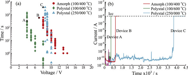
Figure 2. (a) Forming time (tform) as a function of applied voltage bias (Vform) for devices based on 30 nm HfO2 films with varying heat treatments and microstructures. (b) Current-time traces for selected devices (A, B, and C) from each microstructural category/heat treatment.
Download figure:
Standard image High-resolution imageCurrent-time traces of devices selected for AFM imaging are representative of I–t curves obtained for the majority of devices formed, and show similar characteristics, regardless of the crystallinity of the HfO2 layer (figure 2(b)). An initial decay in current associated with charging of the capacitance of the dielectric layer proceeds, followed by either an abrupt or step-like increase in current, until a final breakdown is achieved with current limited at 100 μA. We interpret these intermediate current jumps as the beginning of filament formation as ionic migration of Cu+ into the HfO2 film creates additional sites for electronic Poole–Frenkel hopping conduction or trap assisted tunneling to occur. In some cases, sharp decreases in current are observed as in device C (figure 2(b)). In this case, these fluctuations are attributed to fluctuations in charge trapping and de-trapping. I–t curves in 10 nm films show similar characteristics. Both abrupt and gradual forming traces are observed (figure 2(b)) which may have implications for the initial shape and size of the conductive region.
Resistance of formed devices was measured after the forming operation and results show that as Vform decreases, the resistance of the formed device increases. Here, when devices are formed above 4 V, the resistance of the 'on-state', Ron does not scale with the set compliance current by ohm's law as expected, indicating some overshoot of the compliance current due to charge storage in parasitic elements of the test circuit [47]. Notably, Ron decreases as Vform increases both within and between HfO2 films of differing microstructure (S-figure 3), so that resistance of the conductive filament is primarily controlled by the compliance current overshoot and indirectly, Vform, rather than the electric field across the dielectric or microstructure of the dielectric. Finally, the variability in Ron is uniform across all forming conditions and HfO2 dielectric microstructure groups (σ ∼ 15 kΩ). Therefore, although the principal determinant of resistance state is Icc overshoot, the source of variability could still have several sources: (i) changing capacitance of the test circuits between runs (ii) materials properties that limit ion migration (iii) materials properties that limit heat transfer.

Figure 3. Deconstruction series of a conductive filament formed in 30 nm thick polycrystalline HfO2 (100 °C/600 °C) at 4 V. (a) AFM topographic imaging of the device top electrode post-forming demonstrates 3 topographic 'hillocks' which are potential conductive filament sites. (b) Schematic of the experimental set-up. (c) Imaging of the area post-etching removal of the top electrode shows that not all hillocks previously observed were below the top electrode, accompanied by (d) a schematic of the device status. Only a single location (e) showed both a topographic hillock associated with (f) a strong conductive signal saturating the amplification circuit, which is smaller in area (0.003 μm2) than the topographic feature (0.025 μm2). (g) A schematic of the potential forming mechanism showing that as Cu ions migrate toward the bottom electrode, the HfO2 matrix is displaced upwards, while a high current density flowing from grounded bottom electrode to positively biased top electrode causes some electro-migration of the p + Si bottom electrode upwards. Simultaneously, the high electron current density causes a large increase in temperature in the region of the filament, which in turn drives lateral growth of the filament.
Download figure:
Standard image High-resolution image3.3. Device deconstruction and 3D tomography of conductive filaments
3.3.1. Device deconstruction
In order to observe the relative impacts of electric field, Vform, and film microstructure on conductive filament size and shape, a dedicated AFM workflow was developed to deconstruct the formed device layer by layer, and ultimately obtain 3D shape by scratching through the HfO2 matrix in selected devices. Device deconstruction was accompanied by optical microscopy and atomic force microscopy (1) on the top electrode of the device before forming, (2) from the top electrode of the device post-forming, and (3) conductive and topographic AFM imaging of the HfO2 surface post removal of the top electrode. At the Cu top electrode, several topographic features were present in AFM images of the copper top electrode, but were later found not continuous from the HfO2 surface through to the copper top electrode and were therefore interpreted as debris (figure 3(a)). Following removal of the top electrode, conductivity was exclusively used to identify and locate a conductive filament. Notably, all conductive signals were accompanied by some deformation of the HfO2 layers of varying extents, with an oblong 'hillock' ranging from (2 nm to 20 nm) in height found under the lowest Vform conditions (4 V). This observation demonstrates that conductive filament forming is accompanied by physical disruption and localized uplift of the oxide layer, which similarly deforms the Cu layer above it.
A major limitation of AFM techniques is an inability to sample the chemical composition of the structure under study. The composition of these central hillocks is a matter for further investigation, but most likely involves some mixture of copper ions and defective, vacancy rich oxide. As the positive electric field drives metal migration into the oxide layer (as has been evidenced in several TEM-EELS studies [1, 48, 49]), volume expansion of the HfO2 matrix must occur. At such high levels of current density and in the presence of large thermal gradients, it is not inconceivable that Cu downward migration forces some mass extrusion to the free surface (figure 3(e)). This mixed (Hf–Cu–O) composition would then explain the inability of the FeCl3 solution to remove the conductive 'hillock' and completely planarize the bare HfO2 surface. Moreover, expected resistance values calculated from the resistivity of bulk Cu using a simple cylindrical model (area is the minimum measured conductive area and the height is equal to film thickness) yields values six orders of magnitude lower than measured device Ron values (table 2). This discrepancy points to a filament composition that is not purely copper. Finally, the results of TEM studies of gate oxide breakdown suggest that the identified conductive 'hillocks' might in some part be formed by the electro-migration of Si from the bottom electrode [50]. Electrons flowing from the bottom electrode toward the positively biased top electrode at a current density of (J ∼ 1 × 10⁸ A cm−2) could produce an 'electron wind' that causes Si atoms to migrate into and across the oxide layer. Such migration, termed dielectric breakdown induced epitaxy (DBIE), has been found to be the major microstructural defect in cases of hard dielectric breakdown in a wide variety of gate oxides (Si3N, SiO2, HfO2) [51–53]. In these oxide layers (3–5 nm thick), DBIE defects are observed using voltages as low as 2.5 V and compliance currents as low as 10 μA–50 μA. In these voltage ranges, the metallic spiking desirable for resistance switching cannot be isolated from DBIE [53]. Thus, the chemical nature of the observed deformation of the oxide layer and conductive filament is proposed to be some mixture of Hf, O, Cu, and Si, although a uniform composition throughout is not necessarily supported. Further TEM-EELS sample preparation and characterization would be required to definitively establish the composition of the region.
Table 2. Electrical forming characteristics for devices used in 3D scratch-through experiments.
| Filament | HfO2 thickness | Vform | tform (s) | Ron (kΩ) |
|---|---|---|---|---|
| A | 10 | 4 | 102 | 23.8 |
| B | 10 | 4 | 10 | 83.4 |
| C | 10 | 4 | 76 | 44.4 |
| D | 30 | 4 | 1408 | 6.7 |
3.3.2. 3D Tomograms
Following this initial deconstruction, selected devices were chosen for further investigation to establish the 3D shape of the formed conductive filaments. While 2D scans can give insight into area scaling at the top of the filament and filament location, subsequent switching parameters (Vreset, Vset, and the resistance states) are determined by the narrowest diameter and shape of a filament which could be buried within the matrix of the dielectric layer. In 10 nm thick and 30 nm thick polycrystalline HfO2 films with devices formed at 4 V and compliance current of 100 μA, no macroscopic damage to the Cu top electrode or to the underlying HfO2 films was observed by optical microscopy. Instead, the filament location corresponds to a topographic hillock (2–17 nm) above the plane of the HfO2 film. Devices formed under these conditions were therefore chosen to study conductive filaments in the absence of catastrophic dielectric breakdown mechanisms.
Etch-wells were created over the course of more than 100 scans until the bottom electrode was reached and identified by the appearance of weak conductive signal across the bottom of the well. Etch removal rates were variant over both space and time. As the diamond AFM tip removed material from the initial hillock during the first several scans, the overall height of the scan area was increased by 1 nm, rather than decreased, indicative of the redistribution of material from the original hillock position. Following this process, the depth of the scratch through well increased at a decreasing rate, related to the progressive dulling of the conductive AFM tip. A removal rate of approximately 0.1–0.3 nm scan−1 was achieved with AFM set-point of 0.4 V, extracted by linear interpolation between the etch-well depth measured by periodic wide scans. In later cases, the contact force was gradually increased between wide scans in order to maintain a near constant etch rate. In all cases, the conductive signal saturates the AFM circuit (12 nA) and is contiguous throughout the scan area. Although drift of the conductive area is noticeable as an artifact of unavoidable thermal sample drift during AFM imaging over a period of several hours, the boundaries of the conductive region do not change drastically between individual scans—indicating a small spatial uncertainty. Because an excessive contact force is employed to remove HfO2 during scanning, it unlikely that filament area is underestimated due to poor tip-sample contact.
Conductive filament shape was studied in three conductive filaments in 10 nm thick polycrystalline HfO2 layers (250/400 °C). Reconstructed tomograms show a wide degree of variability in shape, but also show that the filaments are similar in size and share a few common features. Topography maps initially showed oblong conductive regions associated with hillocks with dimensions lengths (100–300 nm) and width (50–75 nm). As the diamond tip begins to etch into the HfO2 surface, conductivity narrows and expands non-uniformly approaching the bottom electrode (figure 4). Moreover, the location of the conductive spot seems to be more readily removed with the progression of the initial hillock into a shallow pit at the location of the conductive region, indicative of material mechanically weaker and more defect filled than that of the surrounding matrix. In all cases, the overall dimensions of the conductive signal is smaller than the topographic features it is associated with, indicating that not all of the deformed and defect rich region is highly conductive. Topographic data simultaneously collected was used to correct the conductive signal of the scans, so that reinterpreted 2D bisection of the conductive volume yields the true shape of the filament (figure 4(d)). The final dimensions of the filaments is relatively similar with an overall oblong shape and maximum dimensions of (∼100 nm × ∼50 nm). Here, the largest dimensions of these 'filaments' far exceed the median grain size (∼25 nm) for these films, with even the narrowest points approaching the width of a single grain. Clearly, whatever route along a grain boundary ionic migration may have initially taken, this route was subsumed in the expansion of the filament laterally and vertically during forming. Here, the large temperature gradients caused by high current densities flowing through the nascent filament serve to broaden conductive filaments laterally and become the principal determinants of the maximum filament radii.
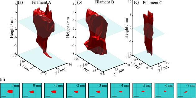
Figure 4. Three separate filaments in 10 nm thick polycrystalline (250 °C/400 °C) HfO2 films formed under nominally the same conditions (4 V, Icc = 100 μA). Distinct morphologies include, (a) an inverse conical shape, (b) a cylindrical shape, and (c) a branched shape intersecting the surface. (d) Topography corrected 2D conductivity maps for filament A, sampled at 1 nm intervals along the height of the filament, with 0 nm referencing the bare HfO2 surface. The inset scale bar corresponds to 32.5 nm.
Download figure:
Standard image High-resolution imageDespite these similarities, a comparison in shape between three filaments formed under identical conditions shows the wide degree of variation in shape expected from measured device Ron values (table 2). In filament A, an inverted cone shape is apparent as conductivity narrows from the HfO2 surface (0 nm) to the bottom electrode reaching ∼20 nm in diameter at its narrowest point, as can be seen in the tomogram (figures 4(a), (d)). Filament B is more cylindrical in nature, albeit with some regions narrowing around −3 nm. Filament C is the most distinctively different in shape from the others, with a narrow cylindrical shape which branches above the HfO2 surface (figure 4(c)). At least one of the filaments (Filament A) demonstrates the inverse cone shape expected from the accepted electrochemical metallization model [6, 8], where the broad base of the cone is associated with the electro-active filament (in this case, Cu). This same structure has been observed previously in a conductive filament in an amorphous HfO2 dielectric layer, where in this case, the electro-active electrode was metallic Hf [54]. Interestingly, in this study, observations of multiple conductive filaments results in other geometries which deviate strongly from this expected shape. This observation of deviation from the accepted model may stem from thermally driven filament broadening, while the wide range of shapes encountered in filament formed under identical electrical stress conditions could stem from (i) differences in initial ionic migration routes, due in part to the structure of the dielectric layer (ii) differences in heat transfer and thermal gradients through the oxide layer or electrodes [55], or (iii) differences in stored parasitic capacitances. Here, the final size and shape of the filament formed under the present electrical bias conditions (representative of device testing conditions in many other studies [56–58]) is likely determined by potent thermal driving forces during the broadening phase of the filament, which are themselves susceptible to several sources of variability.
The conductive filament shape formed under equivalent bias (Vform = 4 V) within a 30 nm thick oxide layer was also examined and compared with results obtained in 10 nm films. At lower electric field (1.3 MV cm−1) in the 30 nm thick randomly oriented polycrystalline HfO2 film (100 °C/600 °C), the conductive filament (figure 5) is larger in area as compared with the filaments in 10 nm films (figure 4), corresponding to the lower measured resistance of the device (table 2). The initial height of the hillock was 17.8 nm tall and required several scans itself to remove. The dimensions of the filament at its' largest point near the HfO2 interface and at the bottom electrode are on the order of 150 nm × 50 nm. The filament's narrowest point (20 nm in radius) corresponds to the intersection of the HfO2 surface, and rather than being the true shape of the filament, it is likely that redistribution of the material from the scribed away hillock limits the conductive signal area in this region. In contrast to the shape of the filaments in the thinner films, the area of the filament does not decrease progressing toward the bottom electrode, but instead remains fairly constant until splitting into several branches intersecting the bottom electrode (figure 5). Although the entire thickness of the film was not able to be removed before dulling of the diamond tip precluded further scratching (final depth of the well was 28 nm), it is likely that a continuation of the branches would be observed penetrating into the p + Si bottom electrode. As in the 10 nm thick films, the shape of the conductive filament deviates strongly from the expected inverse conical shape under the given electroforming conditions. However, given the variability observed between different filament shapes in 10 nm films (despite forming under identical conditions), it is important not to over-interpret distinctions between filaments observed in 10 nm films versus those observed in 30 nm films.
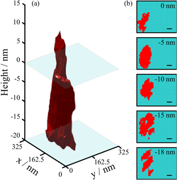
Figure 5. (a) 3D reconstruction of a filament formed in 30 nm polycrystalline HfO2 film (100 °C/600 °C) at 4 V, Icc = 100 μA, and (b) accompanying 2D scans extracted at given height intervals. The scale bar corresponds to 32.5 nm.
Download figure:
Standard image High-resolution image3.4. Extent of deformation: from filament structures to catastrophic breakdown
In order to determine the relative impacts of Vform, electric field, and HfO2 film microstructure on the deformation caused by uncontrolled mass flux during device forming, a combination of optical microscopy and atomic force microscopy was used to observe first the copper top electrode and then the uncovered dielectric layer. The extent of deformation lies along a spectrum from nm scale uplift of the Cu top electrode and HfO2 layer deformation to micron scale catastrophic disruption and melting away of the top electrode, implicating thermal dielectric breakdown mechanisms. Importantly, the area of the damage scales with Vform and the scaling is relatively unaffected by HfO2 layer microstructure or film thickness i.e. electric field (figure 6; S-figures 4–6).

Figure 6. Mean area of dielectric breakdown calculated from optical microscopy images at 100X magnification at each applied forming bias. Outliers in each series are plotted as an 'X'. Inset: a characteristic device from 30 nm polycrystalline (250/--- °C) films showing disruption of the thin (25 nm) copper top contact.
Download figure:
Standard image High-resolution imageIn all devices formed above 5 V, the copper top electrode appears to have melted in a ridge surrounding a depression in the HfO2 layer (figure 6 inset). Optical Microscopy and AFM topographic imaging of device top electrodes revealed linearly increasing melt area as forming voltage increased within each oxide microstructure series in 30 nm HfO2 films (figure 6). Between oxide microstructure series, and over the full range of forming voltages, a few common features were observable in dielectric breakdown spots. In amorphous oxides (100/400 °C), as the forming bias increases between 7 V and 14 V, the oxide breakdown observed on the edges of devices grows in area from ∼1 μm2 at 7 V to ∼10 μm2 at 14 V (figure 6). In oriented polycrystalline HfO2 films (250/--- °C), damage areas range from (∼0.2 to 2) μm2 at 8 V and 10 V, respectively. In the more randomly oriented polycrystalline film (100/600 °C) cumulative damage area scales from 500 nm2 at 4 V to 2 μm2 at 8 V. In many cases, devices in this film formed at (4–5) V showed no penetration of the copper top electrode optically. However, AFM imaging of the top electrode later revealed the presence of (10–30) nm hillocks which deformed, but did not penetrate the 25 nm thick copper top electrode.
The morphology of the breakdown in the HfO2 dielectric layer is similar to breakdown morphologies observed in capacitance failure and gate oxide failures in MOS-caps. A small hillock (3–50 nm in height and 50–500 nm in width) is observed before and after the removal of the copper electrode in all samples (figure 3) and over all forming voltages. It is likely that this hillock represents the initial site of breakdown with damage irradiating outward from this site. In devices formed above 5 V, this hillock is surrounded by a pit, which in some cases penetrates into the p+Si substrate. The area and depth of this pit also scales with forming voltage, ranging from (∼1 to 3) μm2 (figure 7; S-figures 4–6). Within each oxide microstructure series, the area of the damage scales with Vform (figure 7; S-figures 4–6), with the most dramatic breakdown structures observed in 30 nm amorphous HfO2 films (Vform = 14 V) and minimized in polycrystalline films at 4 V with 'hillocks' 2 nm–30 nm tall. Thus, damage in the HfO2 dielectric layer shows the same trends in scaling with Vform as top electrode melting and is indicative of redistribution of the dielectric layer along a spectrum, from simple expansion/extrusion at 4 V to increasing mass loss at 14 V.
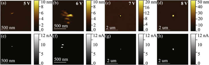
Figure 7. AFM Characterization of the bare HfO2 surface in deconstructed devices based on a 10 nm thick polycrystalline HfO2 layer (250 °C/400 °C) formed at a range of Vform. AFM topographic images demonstrate increasing areas of mass redistribution as a function of increasing Vform from (a) 5 V, (b) 6 V, (c) 7 V, and (d) 8 V. Topographic images are accompanied by (e)–(h) their corresponding c-AFM images.
Download figure:
Standard image High-resolution image
The primary mechanism for the massive damage of the HfO2 layer and Cu top electrode observed optically and by AFM is frequently encountered in studies of capacitor breakdown and gate oxide breakdown, as well as during electrostatic discharge (ESD) events [49, 53, 59–61]. As the resistance of the device under test transitions from the initial high resistance state to the final low resistance state within hundreds of ns, parasitic capacitance in the testing equipment and the contact pad of the device (estimated around ∼1 nF), discharges a large current into the device. Measurement of discharge currents at ns time scales has shown that this overshoot can range from 10 to 100 times the compliance current [47, 62, 63]. The solution widely adopted includes integration of a transistor or diode lithographically connected to the device on chip, so that the area which accumulates stray capacitance is minimized. However, it has also been shown that parasitic currents can be limited via reduction of applied forming voltage indirectly by increasing the discharge time and reducing the amplitude of the discharge peak [64]. The magnitude of this current was not measured as in other studies, but can be estimated from the reset current (Ireset) obtained in the subsequent cycle by the relationship Iset ≈ Ireset. In tested devices, Ireset ranged between 1 mA and 10 mA, indicating that the parasitic current overshoot was at least 10 times greater than the set Icc of 100 μA when Vform > 4 V. At it is lowest levels, this uncontrolled current discharge then causes local heating via joule heating, driving ion diffusion leading to broadening of the conductive filament. At the other extreme, temperatures reached are high enough to participate in a feedback loop of catastrophic dielectric breakdown. As electrons release heat passing through the dielectric layer, more defects are thermally created, which in turn allow even more electrons to flow through the breakdown location, eventually leading to the observed catastrophic breakdown structures.
Between HfO2 films with different initial microstructure tested at an identical Vform (8 V), the morphology of the breakdown differs in shape and in location (S-figure 7). In amorphous HfO2 films, damage occurs only at the edge of devices so that the central hillock is surrounded by a semicircle of missing HfO2 material, penetrating down to 30 nm through the p + Si bottom electrode. In more oriented polycrystalline film, the site is within the interior of the device electrode, and encompasses a hillock surrounded by a bowl, again penetrating through the depth of the bottom electrode. Finally, in more randomly oriented polycrystalline films, several shallow sites are identified with a central hillock. The randomly oriented grain structure of the polycrystalline (100/600 °C) film provides for significantly different damage morphology than that observed in the amorphous (100/400 °C) and more oriented polycrystalline (250/--- °C) films. Copper migration is energetically favored along several different grain boundary pathways, leading to the observation of multiple breakdown spots. Moreover, the total device current is divided and reduced in each separate parallel branch in the case of multiple filaments, resulting in a smaller damage extent at each location. Therefore, while Vform is the principal determinant of damage area and depth, the microstructure of the oxide layer determines the location and multiplicity of disruption.
Although these observations of top electrode melting and oxide disruption dependence on Vform have already been extensively explored in the context of the wide body of dielectric breakdown literature, the implications for resistance switching device based studies are not inconsequential. While it has been demonstrated that parasitic discharges and Iset/Ireset can be controlled below 10 μA with lithographically integrated transistors or diodes [65], some amount of thermal energy dissipation is still required during reset operations or even during the initial filament forming operation. Many groups report relatively large compliance currents (Icc ≥ 100 μA) in order to achieve stable Ron states and Ron/Roff > 103 [24, 57, 66–69], suggesting that thermal dielectric breakdown mechanisms observed in this work might also be observed in studies in which large on/off ratios are reported with limited device cycles. As shown, these mechanisms are highly destructive to the oxide layer and contribute a large degree of variability in physical size/shape of damage spots, possibly occluding the impact of tested variables.
4. Conclusion
In conclusion, the 3D shape of conductive filaments formed in p+Si/HfO2/Cu ECM devices based on a polycrystalline HfO2 layer has been explored with a scalpel c-AFM tomography technique. Results for filaments formed under identical conditions show a range of shapes including conical, cylindrical, and branched, which deviate from the exclusively inverted-cone shape predicted by the phenomenological electrochemical model [6]. Thermal broadening of the filament caused by compliance current overshoot is strongly implicated in this shape deviation by the observation of an increasing spectrum of HfO2 film damage with increasing forming voltage (and not electric field). Here, the amplitude and duration of compliance current overshoot scales with Vform, and thus the thermal energy released into the confined filament region scales with Vform. At the lowest voltage (4 V), filament formation is accompanied by minimal uplift of the HfO2 dielectric film and Cu top electrode, while at the highest voltage (14 V) catastrophic mass removal is observed. Finally, the role of microstructure is shown to be to direct the location of filament forming sites, while Vform directs the ultimate size of the filaments or damage. Thus, we demonstrate that the original shape of the conductive filaments is strongly impacted by joule heating during the forming step under common forming conditions, so that the simple geometry assumed in many conductive filament modeling studies may no longer be an acceptable assumption in many cases.
Acknowledgments
The authors gratefully acknowledge the use of AFRL cleanroom facilities and the aid of Dr. Kevin Leedy in ALD of HfO2 thin films. This work has been supported by AFOSR LRIR 14RX13COR. The authors also wish to acknowledge Sarah Hammock for aid in early device electrical characterization and atomic force microscopy characterization.