

Abstract
Semiconducting metal oxide gas sensors typically operate at a high temperature and consume hundreds of milliwatts of power. Therefore there is great demand for the development of a low-power gas-sensing technology that can sensitively and selectively detect the gas analytes present in the atmosphere. We report an ultralow-power nanosensor array platform, integrated with an independently controlled nanoheater of size 4 μm × 100 nm, which consumes ∼1.8 mW power when operated continuously at 300 °C. The heaters exhibit a fast thermal response time of less than 1 μs, and can be utilized to operate in duty cycle mode, leading to power saving. The active area of the nanosensor is 1 μm × 200 nm, defined by sensing electrodes with a nanogap of ∼200nm, leading to small form factor. As a proof of concept, each of the sensing elements in the array is functionalized with different sensing materials to demonstrate a low-power, sensitive and selective multiplexed gas-sensing technology for the simultaneous detection of CO (∼93.2% for 3 ppm at 300 °C), CO2 (∼76.3% for 1000 ppm at 265 °C), NO2 (∼2301% for 3 ppm at 150 °C) and SO2 (∼94% for 3 ppm at 265 °C). The technology described here uses scalable crossbar architecture for sensor elements, thus enabling the integration of additional sensing materials and making it customizable for specific applications.
Export citation and abstract BibTeX RIS
1. Introduction
Metal oxide gas sensors based on microelectromechanical systems (MEMS) are very promising due to their low cost, miniaturization and ease of fabrication, and can be compatible with CMOS integrated circuits. These devices show well-known limitations such as poor selectivity and sensor signal drift. Another issue is associated with the relatively high power consumption of the microheaters (in the range of a few tens of milliwatts) as metal oxide sensors require a high temperature for operation [1–3]. The selectivity issue can be resolved by integrating the sensors in an array form with the provision for operating each sensor independently. The issue of high power consumption can be solved by integrating on a sensor chip a miniaturized and thermally isolated heater underneath the sensing material to control the operating temperature. Two approaches have been widely used to thermally isolate the heater from bulk silicon, i.e. surface and bulk-micromachining processes [4, 5]. In general, surface micromachined released MEMS structures are often said to be less fragile than bulk micromachined released MEMS structures, which are challenging to package [1]. This helps to reduce the power consumption of the heater, but tens of milliwatts are still required to drive the heater to about 300 °C [2, 6]. Dai et al [7] have reported that a Pt-based microheater, surface wet (KOH) etch released, consumes ∼34 mW power to heat the sensor chip to 368 °C. Moon et al [8] have fabricated a CO microgas sensor based on SnO2 nanopowders and the power consumed by the microheater, bulk micromachined released with KOH, is ∼14 mW to attain a working temperature of 400 °C. Zhou et al [9] have developed a semiconductor metal oxide sensor integrated with a surface micromachined KOH released microheater which consumes ∼34 mW at 950 °C. So there is a need to develop a gas sensor array with low-power consumption, independent control of sensor temperature, high sensitivity and selectivity, the lowest possible limit of detection, fast response time and high response stability.
Here, we present an integrated 2 × 2 nanosensor array on a single chip with four independent nanoheaters based on Pt/Ti for individual temperature control of four sensing elements; ZnO, WO3, BaTiO3–CuO doped with 1% Ag and V2O5 for selective detection of CO, NO2, CO2 and SO2 gases, respectively. The optimum film thickness of the sensing materials is realized through a RF-sputtering process. Nanoheaters are isotropically released in their localized heating zone to minimize power consumption. The integration of sensor arrays and nanoheaters is realized using a simple crossbar architecture. The specific scientific and technological advances include: (i) miniaturization to achieve low thermal mass sensors, that are extremely power efficient; (ii) a simple scalable busbar architecture analogous to high-density semiconductor memories; (iii) a surface micromachining process to achieve high manufacturing yield, in contrast to the conventional bulk-micromachining approach; and (iv) fast response and recovery time for the sensors, enabling a pulsed mode of sensor operation.
2. Device design and fabrication
A sensor array device with four nanosensors has been designed and fabricated. Four identical nanoheaters of dimensions 4 μm × 100 nm are integrated with each sensor in an array on a chip size of 1 mm × 1 mm to minimize the device area and also to achieve independent temperature control over the four sensing materials. Each sensor of the array has a nanogap electrode gap of ∼200 nm to measure the electrical signal received from the sensing material. This nanogap electrode helps to achieve fast response and recovery times [7]. The active area of each sensor is 1 μm × 200 nm, and the active area is isotropically released to reduce the power consumption of the nanoheater.
The nanosensor array is fabricated on a single-sided polished p-type (100) Si substrate of thickness 380 μm. The schematic flow of sensor fabrication is shown in figure 1. Thermally grown 60 nm thick SiO2 is used as an insulator on a pre-cleaned Si substrate. The SiO2 layer serves as a sacrificial layer to release the active sensor area. Initially, the nanoheater array is patterned using electron-beam lithography (EBL) on a polymethylmethacrylate (PMMA)-coated SiO2/Si substrate. MIBK:IPA (methyl isobutyl ketone:isopropyl alcohol, 1:3) solution is used to develop the heater pattern. The nanoheater array of Ti/Pt (10/50 nm) is realized using dc-sputtering followed by a lift-off process. On top of the heater, a ∼120 nm thick e-beam evaporated SiO2 layer is selectively deposited using a second EBL step to serve as an electrical insulator between the nanoheater and sensing electrodes. The sensor electrodes and the heater electrodes are designed such that we avoid the cross-over of metal lines by providing an offset in the layout. Then, sensing electrodes with nanogap of ∼200 nm for each sensor in the array are patterned and fabricated using a third EBL step and dc-sputtering of 60 nm thick Ti/Pt (10/50 nm). This is followed by four lithography steps along with a RF-sputtering process and lift-off to define each of the sensing elements on top of the sensing electrodes; the area of sensing material deposition is 8 μm (length) × 500 nm (width) for each sensing layer. Figure 2(a) shows a field emission scanning electron microscope (FESEM) image of the fabricated 2 × 2 nanosensor array device and figure 2(b) shows a tilted view of an unreleased single nanosensor. For better power performance the nanoheater should be isolated from bulk silicon, and hence the SiO2 underneath the nanoheater is isotropically etched by fluorine chemistry (CF4 50 sccm, RF power 100 W, pressure 100 mTorr) in a reactive ion etching process [10, 11]. During the structural release, the resist mask (PMMA A4 and PMMA C6) ensures the protection of the active area of the nanosensor array. Figure 2(c) indicates the isotropic locally released nanosensor. Figure 2(d) shows a SEM image of the nanoheater, passivated with SiO2 and with the sensing electrode perpendicular to the nanoheater (crossbar architecture).
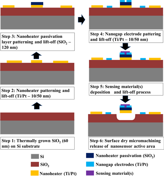
Figure 1. Two-dimensional representation of the nanosensor array fabrication flow.
Download figure:
Standard image High-resolution image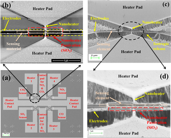
Figure 2. (a) Fabricated 2 × 2 nanosensor array. (b) Tilted-view of an unreleased single nanosensor. (c) Tilted-view of an isotropically released device. (d) Zoomed tilted view of the released device, indicating the passivation oxide, sensing element and nanoheater with sensing electrodes.
Download figure:
Standard image High-resolution image3. Results and discussion
3.1. Nanoheater characterization
Measurement of the temperature dependence of the resistance of the nanoheater is done using the hot chuck of a Cascade probe station with internal feedback control of temperature with an accuracy of ±1 °C. In addition, a Keithley 2400 source meter with four-wire resistance configuration was used to minimize the lead resistance error. The temperature coefficient of resistance (TCR) of the nanoheater is 1.37 × 10⁻³ °C–1 (figure 3(a)) which is ∼2.5 times less than the TCR bulk value of Pt (3.73 × 10⁻³ °C–1) [12].

Figure 3. (a) Temperature coefficient of resistance of a Ti/Pt nanoheater. (b) Temperature versus power relation of the released nanoheater. (c) Thermal time constant of the fabricated released nanoheater (rise time 165 ns, fall time 160 ns).
Download figure:
Standard image High-resolution imageCoventorWare [13] thermoelectrical simulation of a nanoheater suggested that a 60 nm airgap provides effective thermal isolation for the nanoheater from the bulk silicon substrate. Based on electrothermal simulations, an airgap of 60 nm was found to be adequate to provide partial thermal isolation for the nanoheater (supplementary information S1 available online at stacks.iop.org/NANO/31/025301/mmedia). This is also verified by the experimentally estimated power values for the released nanoheater. As shown in figure 3(b), the nanoheater consumes ∼1.8 mW to reach 300 °C and ∼3.4 mW to reach 500 °C. The simulated temperature of the released nanoheater is in good agreement with experimentally observed temperature values. The thermal simulation of different heater widths with a fixed metal thickness of 60 nm is provided in supplementary information S2. In conclusion, a 100 nm wide and 60 nm thick Pt heater shows very high temperature generation (> 200 °C) at a significantly very low-power of <1 mW. Moreover, a 100 nm wide nanoheater with a 60 nm thick Pt layer shows high mechanical stability during fabrication of the sensor chip.
The fast pulse I–V measurement shown in figure 3(c) indicates that the fabricated nanoheaters have a very low thermal time constant. The ringing behavior is probably due to probe inductance and capacitance. Nonetheless, we can conservatively estimate the time constant to be in the range of a few 100 ns (less than 1 μs).
Such a short thermal time constant allows the nanoheater to operate with a low duty cycle, leading to power saving. The infrared image of the released nanoheater, powered with ∼3.4 mW (image not included here), depicts it as a bright localized heat reservoir. Due to the low magnification of the infrared camera, accurate temperature measurement of the nanoheater could not be done.
3.2. Characterization of the sensing material
The thin film of each sensing material, ZnO for a CO sensor, BaTiO3–CuO doped with 1% Ag for a CO2 sensor, WO3 for a NO2 sensor and V2O5 for a SO2 sensor, is optimized by the RF-sputtering process for stable and selective sensor response prior to deposition on nanosensor array. The detailed process of thickness optimization of sensing films, material characterization and extensive thickness-dependent sensing characterizations of each metal oxide film is carried out before integration on the nanosensor array devices [12, 14, 15]. The optimum film thickness, ∼21 nm for ZnO film, ∼185 nm for BaTiO3–CuO doped with 1% Ag, ∼85 nm for WO3 film and ∼61 nm for V2O5 film, can be accommodated on nanosensor electrodes with a 200 nm nanogap. In brief, films were characterized by x-ray photoelectron spectroscopy and FESEM-energy dispersive analysis and found to be of the desired form.
3.3. Gas-sensing characteristics
The nanosensor array was used to measure the selective response for CO, CO2, NO2 and SO2 gas with the respective sensing elements. The sensor is mounted inside a gas-sensing chamber, details of which are described in supplementary information S3. The nanosensor device is wire-bonded to a printed circuit board to facilitate the gas-sensing measurement. The gas chamber has the provision to connect the target gas cylinder with synthetic air cylinder to set the appropriate concentration of target gas. Two mass flow controllers are used to set the gas flows for synthetic air (reference gas) and the target gas. The response of sensor is been defined as the ratio of change in film resistance upon exposure to the test gas (Rg) to the film resistance in air (Ra) at same operating temperature, and is calculated using the following equation [12]:

where Ra is the resistance of sensor in air and Rg is the resistance of the sensor in the test gas at the same operating temperature. The sensor array has been extensively characterized by operating individual sensors separately and is shown to have very good sensitivity and selectivity.
3.3.1. ZnO-based CO nanosensor
The resistance of ZnO film was found to decrease on exposure to CO, which is a reducing gas, as shown in figure 4. The ZnO-based nanosensor exhibits a fairly linear response of 27.3%/ppm in the low concentration range of 0 to 3 ppm CO, while the response of 4.7%/ppm is found in the higher concentration (>3 ppm) range, as shown in the response versus concentration plot in the inset of figure 4. The slower response in the higher CO concentration range may be due to the saturation limit of this ZnO-based nanosensor. A high response (∼93.2%) is observed upon exposure to 5 ppm CO at an optimum operating temperature of 300 °C (∼1.8 mW). The response and recovery times of the nanosensor are ∼65 s and ∼94 s, respectively. These times are short enough for practical applications of this sensor. The fabricated nanosensor shows high selectivity towards CO in the presence of other interfering gases, as shown in bar plot in the inset of figure 4.
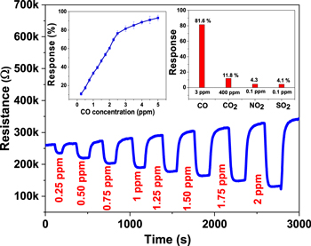
Figure 4. CO concentration-dependent dynamic characteristics of the ZnO-based nanosensor at an operating temperature of 300 °C (∼1.8 mW). Inset: the response versus CO concentration plot and selective response characteristics of the nanosensor.
Download figure:
Standard image High-resolution imageThe ZnO nanosensor is able to detect a CO concentration of 250 ppb, which is comparatively lower concentration than that reported in other studies [16–30]. Figure 5 shows a comparison of the responses of the present sensor at different CO levels along with the responses observed by other researchers [16–30]. The ZnO-based CO nanosensor fabricated in the present investigation shows high sensitivity with selective detection towards CO and a quick response and recovery time.

Figure 5. CO response and operating temperature (red, >300 °C; green, 200–300 °C; black, 25–200 °C) data from the literature, compared with the present ZnO-based nanosensor.
Download figure:
Standard image High-resolution image3.3.2. BaTiO3-CuO doped with 1% Ag for CO2 nanosensor
Figure 6 shows the CO2-sensing characteristics of the nanosensor based on BaTiO3–CuO film doped with 1% Ag, recorded at an operating temperature of 228 °C (∼1.3 mW). The sensor showed a linear response of 9%/100 ppm for CO2 concentrations varying from 300 to 1000 ppm, as shown in response versus CO concentration plot in the inset of figure 6. The sensor attains a maximum response of ∼76.3% to 1000 ppm CO2 at 228 °C. In addition, the response time of the sensor at various CO2 concentrations is in the range of ∼300 s to ∼360 s. The fabricated sensor also showed a highly repeatable response to a fixed CO2 exposure of 1000 ppm. The BaTiO3–CuO (1 wt% Ag)-based nanosensor shows high selectivity towards CO2 gas, as represented in the inset of figure 6.
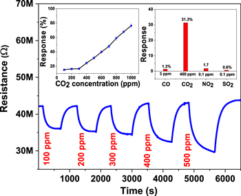
Figure 6. CO2 concentration-dependent dynamic characteristics of the BaTiO3–CuO (1 wt% Ag)-based nanosensor at an operating temperature of 228 °C (∼1.3 mW). Inset: the response versus CO2 concentration plot and selective response characteristics of the nanosensor.
Download figure:
Standard image High-resolution imageTo estimate the low order of detection of CO2, the gas concentration was tested from 100 ppm to 1000 ppm and also compared with the already reported results. Figure 7 shows a comparison of the as-fabricated sensor responses at different CO2 levels along with the responses observed by other researchers [15, 31–41]. In summary, the present investigation of the characteristics of BaTiO3–CuO (1 wt% Ag)-based CO2 suggests that the fabricated nanosensor achieves high sensitivity and selectivity with quick response and recovery times.

Figure 7. CO2 response and operating temperature (red, >300 °C; green, 200–300 °C; black, 25–200 °C) data from the literature, compared with present BaTiO3–CuO-based nanosensor.
Download figure:
Standard image High-resolution image3.3.3. WO3 nanosensor for NO2
On exposure to NO2 gas at an optimum sensor operating temperature of 150 °C, the resistance of the film is found to increase due to the oxidizing nature of the gas, as shown in figure 8. Response versus temperature measurement of the fabricated sensor revealed that the WO3 film-based sensor shows its highest response (∼2301%) at 150 °C (∼0.8 mW) for a NO2 concentration of 3 ppm. Fabricated sensors were also exposed to different NO2 concentrations from 0.1 to 3 ppm. There was a sudden increase in response at a low NO2 concentration (<0.5 ppm), and on further exposure to higher concentration the sensor responded comparatively slowly, as shown in the response versus concentration graph in the inset of figure 8. Moreover, the fabricated sensor shows selective response towards NO2 in the presence of other interfering gases (shown in the inset of figure 8). In addition, the response times of the sensor at various NO2 concentrations are in the range of ∼8 s to ∼11 s.
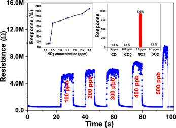
Figure 8. NO2 concentration-dependent dynamic characteristics of the WO3-based nanosensor at an operating temperature of 150 °C (∼0.8 mW). Inset: the response versus NO2 concentration plot and selective response characteristics of the nanosensor.
Download figure:
Standard image High-resolution imageFor a comparison of the present results, the published reports on NO2 sensors are summarized in figure 9 together with the data for present NO2 sensor [42–55]. This comparative NO2 sensing data shows that the NO2 sensor based on WO3 sensing material not only shows a high response at low NO2 concentration but is also capable of detecting NO2 concentrations in air as low as 100 ppb .
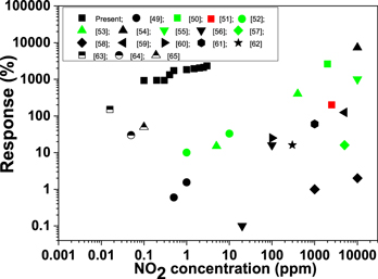
Figure 9. NO2 response and operating temperature (red, >300 °C; green, 200–300 °C; black, 25–200 °C) data from the literature compared with the present WO3-based nanosensor.
Download figure:
Standard image High-resolution image3.3.4. V2O5 nanosensor for SO2
The sensor based on V2O5 sensing material showed its highest response (∼94%) at an operating temperature of 265 °C (∼1.5 mW) for a SO2 concentration of 3 ppm. The sensor signal was recorded for SO2 concentrations from 0.1 to 3 ppm, and shows a fast increase in response up to 0.5 ppm and slower increase at higher concentrations, as shown in response versus concentration plot in the inset of figure 10. The response time of the sensor is found to be in the range of ∼180 s to ∼200 s on exposure to different SO2 levels. Moreover, the sensor shows a repeatable response without any drift in baseline resistance on exposure to a fixed SO2 concentration of 3 ppm. The sensor shows a highly selective response to SO2 in the presence of other gases, as shown in bar plot in the inset of figure 10.
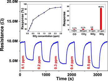
Figure 10. SO2 concentration-dependent dynamic characteristics of the V2O5-based nanosensor at an operating temperature of 265 °C (∼1.5 mW). Inset: the response versus SO2 concentration plot and selective response characteristics of the nanosensor.
Download figure:
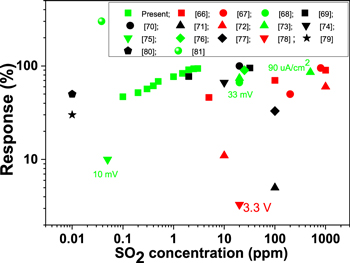
Standard image High-resolution imageThe V2O5-based nanosensor is able to detect a SO2 concentration of 100 ppb, which is a comparatively lower concentration than that reported in other studies. Figure 11 shows a comparison of the responses recorded in the present work at different SO2 levels along with the responses observed by other researchers [56–68].
Figure 11. SO2 response and operating temperature (red, >300 °C; green, 200–300 °C; black, 25–200 °C) data from the literature compared with the present V2O5-based nanosensor.
Download figure:
Standard image High-resolution image
We have summarized the data for three nanosensor array devices to understand the repeatability of fabricated devices. The response of each device is shown in supplementary information S4. The coefficient of variation of all the investigated sensors is below 10% which assures good repeatability across fabricated nanosensor array devices.
4. Conclusion
In conclusion, a highly sensitive, selective and low-power 2 × 2 sensor array platform is realized with four independently controlled nanoheaters and 200 nm gap sensing electrodes bridged with optimized metal oxide sensing materials using MEMS-compatible processing. The miniaturized nanoheater of an array consumes only ∼1.8 mW power to achieve a temperature of ∼300 °C. The nanosensor array showed its maximum repeatable response to CO gas (∼93.2% for 3 ppm), CO2 (∼76.3% for 1000 ppm), NO2 (∼2301% for 3 ppm) and SO2 (∼94% for 3 ppm) at operating temperatures of 300 °C (∼1.8 mW), 228 °C (∼1.3 mW), 150 °C (∼0.8 mW) and 265 °C (∼1.5 mW), respectively. The choice of sensing elements of the nanosensor array gives fairly good cross-sensitivity performance in the presence of other interfering gases.
Acknowledgments
We thank MeitY, INAE and DST-SERB for funding support. We also acknowledge the technical support provided by the technical staff in the National Nano Fabrication Facility (NNFC), Micro and Nano Characterization Facility (MNCF) and Packaging lab at the Centre for Nano Science and Engineering (CeNSE), Indian Institute of Science, Bangalore, India.