

Abstract
Driven by the rapid development of novel active-matrix displays, thin-film transistors (TFTs) based on metal-oxide (MO) semiconductors have drawn great attention during recent years. N-type MO TFTs manufactured through vacuum-based processes have the advantages of higher mobility compared to the amorphous silicon TFTs, better uniformity and lower processing temperature compared to the polysilicon TFTs, and visible light transparency which is suitable for transparent electronic devices, etc. However, the fabrication cost is high owing to the expensive and complicated vacuum-based systems. In contrast, solution process has the advantages of low cost, high throughput, and easy chemical composition control. In the first part of this review, a brief introduction of solution-processed MO TFTs is given, and the main issues and challenges encountered in this field are discussed. The recent advances in channel layer engineering to obtain the state-of-the-art solution-processed MO TFTs are reviewed and summarized. Afterward, a detailed discussion of the direct patterning methods is presented, including the direct photopatterning and printing techniques. Next, the effect of gate dielectric materials and their interfaces on the performance of the resulting TFTs are surveyed. The last topic is the various applications of solution-processed MO TFTs, from novel displays to sensing, memory devices, etc. Finally, conclusions are drawn and future expectations for solution-processed MO TFTs and their applications are described.
Export citation and abstract BibTeX RIS
1. Introduction
With the accelerating development of flat-panel displays (FPDs), especially the emergence of active-matrix organic light-emitting diode (AMOLED) displays, the paramount position of a-Si thin-film transistors (TFTs) in the FPD backplane has been relentlessly challenged and partially replaced by evolved silicon, low-temperature polycrystalline silicon and metal-oxide (MO) TFTs [1–3].
MO semiconductors, with the advantages of low-temperature process, large-area deposition, low cost and moderate mobility, have made great progress in FPD applications in a relatively short time [4], challenging the conventional silicon not only in conventional applications but also in exploring completely novel areas like transparent and flexible electronics [5, 6].
Unlike the covalent semiconductors (such as a-Si:H) whose carrier transport paths consist of sp3 orbitals with strong directivity, MO semiconductors are regarded as ionic semiconductors, which compose of at least one metal cation of Zn, In, Ga, Sn, and Cd, with electronic configurations of (n − 1)d10ns0 [4]. For amorphous MO semiconductors, n should be greater than or equal to 5 to insure ns orbital overlap; for crystalline MO semiconductors, n can be downgraded to 4. Although the initial attempts for MO-TFTs can date back to the 1960s [7, 8], they had not drawn much attention until about 40 years later, when the research on the transparent electronics began to rise. MO semiconductor is one of the best choices for transparent electronic devices because of the wide-bandgap property [9–14].
In 2003, Hoffman et al fabricated ZnO TFTs by ion beam sputtering on glass substrates with a bottom-gate structure, as shown in figure 1(a). The glass substrate was blanket coated with a 200 nm thick layer of sputtered indium tin oxide (ITO) as the gate electrode and a 220 nm thick layer of aluminum-titanium oxide deposited by atomic layer deposition as the gate dielectric layer [10]. The ZnO channel layer was deposited at room temperature and then subjected to rapid thermal annealing (RTA) at 700 °C in oxygen ambient to decrease the oxygen vacancies and increase the channel resistance. The highest mobility was 2.5 cm2 V−1 s−1, the threshold voltage (Vth) ranged from 10 to 20 V, and the on/off current ratio (on/off) is ∼107. The optical transmission of the proposed ZnO TFTs was about 75% in the visible range, as shown in figure 1(b). Light sensitivity of the ZnO TFTs was reduced by decreasing the ZnO channel layer thickness.
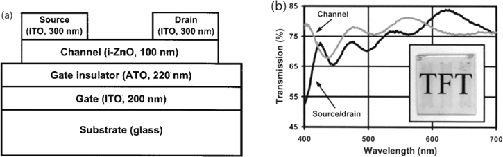
Figure 1. (a) The bottom-gate structure ZnO TFTs proposed by Hoffman et al and (b) their optical transmission spectra for the entire structure including the substrate. Reprinted from [10], with the permission of AIP Publishing.Copyright 2003, AIP Publishing LLC.
Download figure:
Standard image High-resolution imageIn the same year, A TFT with solution-processed ZnO channel layer was successfully fabricated by Norris et al using a superlattice of Al2O3 and TiO2 (ATO) as the gate dielectric and indium-tin oxide (ITO) as the source and drain (S/D) electrodes [15]. An annealing process of 600 °C for 10 min was performed to reduce the oxygen vacancy, and then RTA at 700 °C was carried out to improve the crystallinity of the ZnO thin film. The device showed a mobility of 0.2 cm2 V−1 s−1, but exhibited high sensitivity to light owing to the large surface roughness and grain boundaries.
Although the mobility and transparency of ZnO TFTs are relatively good compared with a-Si and organic TFTs, they usually require high-temperature annealing to improve crystallinity, which is important for electron transport, because there are no overlaps between neighboring Zn4s orbitals. On the other hand, the grain boundary defects inside the polycrystalline film causes a non-uniformity issue in terms of the mobility and threshold voltage, which may prevent the applications of ZnO TFTs to FPDs. Although this non-uniformity of the device parameters may be resolved by introducing a compensation driving pixel circuit, such as a 5 transistors and 2 capacitors pixel circuit, the complexity of the pixel circuit leads to a loss of device yield, a reduce of the aperture, and an increase of the fabrication cost. Therefore, it is particularly urgent to develop new types of MO semiconductors with low annealing temperature, high mobility and good uniformity.
In 2004, Hosono et al demonstrated a transparent TFT on a flexible substrate with near-room-temperature amorphous indium-gallium-zinc oxide (a-IGZO) channel layer [16]. The a-IGZO films were deposited by the pulse laser deposition on polyethylene terephthalate at room temperature, and exhibited Hall mobility exceeding 10 cm2 V−1 s−1, which is an order of magnitude larger than that of a-Si:H. The transparent a-IGZO TFTs with Y2O3 gate dielectric and ITO electrodes (see figure 2) showed field-effect mobilities of 6–9 cm2 V−1 s−1. The flexible TFTs were stable during repetitive bending.

Figure 2. Structure of a-IGZO TFTs fabricated on a plastic sheet and (b) photograph of a flexible transparent TFTs sheet. Reprinted by permission from Macmillan Publishers Ltd: Nature Research [16], Copyright 2004.
Download figure:
Standard image High-resolution imageNomura's work opened the door for amorphous MO semiconductors. As discussed above, the amorphous MO should contain heavy post transition metal cations with (n − 1)d10ns0 (n ≥ 5) electronic configurations. The metal ns orbitals have large radii, leading to an overlap region between adjacent orbitals and considerable band dispersion. Compared to the anisotropic p or d orbitals the spherical symmetry of an s orbital makes delocalized electronic transport less sensitive to the local and extended structural order. As a result, they retain relatively high electron mobility even in amorphous state. A comparison in orbital drawings of Si and MO semiconductors between crystalline and amorphous states is shown in figure 3 [16]. It can be seen intuitively that the electron mobility decreases dramatically from crystal to amorphous state for silicon, while the medium mobility in MO semiconductor is retained even in amorphous state [17, 18].

Figure 3. Schematic orbital drawing of electron pathway in conventional compound semiconductor and MO semiconductor. Reprinted by permission from Macmillan Publishers Ltd: Nature Research [16], Copyright 2004.
Download figure:
Standard image High-resolution imageVarious amorphous MO semiconductors, in addition to IGZO [16, 19, 20], and their corresponding TFTs devices have been investigated, such as indium zinc oxide (IZO) [21], indium tin zinc oxide (ITZO) [22, 23], indium gallium oxide (IGO) [24], etc.
The IGZO has attracted significant worldwide attention for high end AMLCD and AMOLED displays, both from industry and academia, because of its advantages of high mobility, relatively good uniformity, and good scalability to a large substrate size [25, 26]. The IGZO TFTs fabricated with the magnetron sputtering method was commercialized in the AMOLED and AMLCD displays several years ago. However, the conventional vacuum-based techniques require expensive and complicate vacuum deposition and photolithography systems whose maintaining and updating cost is also high. Compared to the conventional vacuum technique, the solution process technique has the merits of low cost, high throughput, and easy chemical composition control [27, 28].
The first solution-processed MO TFT was demonstrated by Ohya et al in 2001 [29]. Since then, there have been many improvements in the solution-processed MO TFTs [30–33]. Evonik Resource Efficiency GmbH developed an impressive large-size solution-based coating method, slot-die coating, for MO TFTs, which is integrated in highly stable OLED display [2]. The proposed Linearcoater and the photograph of the 85 ppi AMOLED display are shown in figure 4. However, there are still some important issues should be addressed for solution-processed MO TFTs before practical applications, such as high-resolution large-area printing, and process-temperature compatibility.

Figure 4. Deposition of iXsenic® solution type semiconductor material via slot-die coating technique and a photography of the AMOLED display. [2] John Wiley & Sons. © 2017 The Society for Information Display.
Download figure:
Standard image High-resolution imageThis review will mainly focus on the latest studies and investigations on solution-processed MO TFTs, and address several major issues including channel layer engineering, annealing methods, patterning methods, gate insulator engineering, and device structures. Firstly, the recent advances in active channel layer engineering to obtain the state-of-the-art solution-processed MO TFTs are reviewed and summarized in section 2. Afterward, in section 3, a detailed discussion on the direct patterning methods is presented, including the direct photopatterning and printing techniques. Next, the effect of gate dielectric materials and their interface on the performance of the resulting TFTs is discussed in section 4. Section 5 is focused on the various novel applications of solution-processed MO. Finally, in section 6, conclusions are drawn and future perspectives for solution-processed MO TFTs and their applications are presented.
2. Active channel engineering
Solution processes of MO semiconductors involve preparing MO precursor solutions or MO nanoparticle suspensions, coating onto the substrates by various methods such as spin coating or printing, and soft baking to remove the solvent followed by post annealing to form a solid film. There are mainly three solution-processing methods for MO semiconductors—nanoparticle suspension method, sol–gel method, and precursor solution method. In this section, the research progress of the three solution-processing methods and the solvent engineering to lower the processing temperature is reviewed and discussed; in addition, the recent progress of the post annealing method, the MO composition and the novel channel structures for solution-processed MO TFTs are summarized.
2.1. Nanoparticle suspension engineering
The nanoparticle (or nanowire) suspension method is to disperse the MO nanoparticles into the solvent with the help of dispersants or surfactant stabilizer to form stable MO nanoparticle suspension, and then to coat onto the substrates followed by annealing steps to remove the solvents and additives [34–37]. The nanoparticle suspension method is attractive in the field of gas sensors, because the nanoparticles have large surface. But its drawback is obvious—because the boundaries between adjacent nanoparticles are so large that the carrier transport paths can be affected seriously. Recently, Dasgupta et al attained surprisingly dense In2O3 nanoparticle thin films and excellent interparticle electrical contacts by adding halide salt flocculation agent to the solution that contained sodium salt of poly acrylic acid (PAANa) [38]. The chemically controlled destabilization and flocculation of the nanoparticles during the ink drying step ensure a nearly complete removal of the organic stabilizer from the nanoparticle surface and then an effective reagglomeration of the printed particles (by the strong capillary force). The TFT with the In2O3 nanoparticle active channel fabricated at room temperature exhibited a mobility of as high as 12.5 cm2 V−1 s−1.
Although great progress has been made to improve the quality nanoparticle film, the challenges are enormous. Perhaps the greatest challenge is how to alloy (dope) the nanoparticles. As discussed above, the binary oxides are not good candidates for TFTs applied to displays, due to their poor uniformity and stability. Thus, to synthesize multicomponent MO nanoparticles with particle size less than 30 nm is important in the future application in displays.
2.2. Sol–gel chemistry engineering
With the concept of 'ceramics from solution', Ebelmen proposed the sol–gel method more than 150 years ago to synthesize silica-based materials using silicon alkoxide precursors [39]. However, this sol–gel method did not attract much attention until about ten years ago. A typical sol–gel chemical reaction route starts with dissolving precursor materials (e.g. metal salts or alkoxides) in an alcohol or aqueous solvent. As depicted in figure 5(a) [39], the solvent molecules (H2O or ROH) solvating metal cations are transformed into hydroxo (OH−) or oxo (O2−) ligands, forming metal hydroxides. Subsequently, a condensation reaction occurs to form M–O–M polymeric frameworks through an oxolation reaction among metal hydroxides. The chemical reaction is shown in figures 5(b) and (c). Generally, three forms of reaction products, sol, gel, and nanoparticles, can be obtained by adjusting the reaction temperature, time, pH value, and catalyst, as shown in figure 6(a) [39]. A xerogel-like oxide thin film can be synthesized by coating the sol–gel precursor solution onto substrates (e.g. spin coating, ink jet printing, and so on), and subjected to a thermal annealing process at a temperature typically above 400 °C in order to complete the condensation reaction, chemical impurities/byproducts removal, and the resulting oxide thin film densification, as depicted in figure 6(b).

Figure 5. Sol–gel chemistry in MO materials. (a) A schematic of reaction between metal ions and water/alcohol molecules to metal hydroxides. Representative chemical reactions are shown for (b) hydrolysis and (c) condensation. Repinted from [39], Copyright 2019, with permission from Elsevier.
Download figure:
Standard image High-resolution image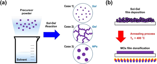
Figure 6. Fabrication of sol–gel MO films. (a) Typical sol–gel MO reaction products (sol, gel, and nanoparticles). (b) A schematic of densifying a sol–gel MO film from as-spun xerogel via high-temperature thermal annealing. Reprinted from [39], Copyright 2019, with permission from Elsevier.
Download figure:
Standard image High-resolution imageAlthough sol–gel method has a long history, it is not the best choice for printing MO-TFTs, because the liquid rheological property of the sol–gel ink changes by time. Meyer et al [40] reported that the stability of the sol–gel ink can be improved (more than 12 h under atmosphere condition) with a sterically encumbering solvent (tetrahydrofurfuryl alcohol), and the In2O3 TFT with this kind of sol–gel ink exhibited a mobility of 9.9 cm2 V−1 s−1. The relatively high ink stability was ascribed to the stronger bonding of tetrahydrofurfuryl alcohol ligands to the alkoxide complex and the resulting reduced ligand exchange kinetic with atmosphere water molecule. However, for practical applications, the stability of the sol–gel ink should still be improved.
To avoid sol–gel aging and to lower the annealing temperature, Sirringhaus et al reported a low-temperature 'sol–gel on chip' method with a soluble metal alkoxide precursor in an aqueous environment [41]. When the metal alkoxide was exposed to the aqueous environment, hydrolysis and condensation processes occurred at a relatively low temperature, as shown in figure 7(a). These decomposition steps required low energy, thus metal-oxide compounds could be achieved at a low temperature. The indium precursor decomposed at a relatively low temperature of 204 °C, whereas the zinc derivative required a higher temperature of 341 °C, as depicted in figure 7(b). However, unwanted precipitation or gel formation was observed in the alkoxide solution due to the high reactivity of the metal alkoxide precursor. This problem can be solved by 'sol–gel on chip' method, using an in situ hydrolyzed process directly on the surface of the spin-coated precursor films. The IZO or IGZO thin films formed by this 'sol–gel on chip' route exhibited smaller number of carbon residues when compared with other routes.

Figure 7. Metal alkoxide molecular precursors. (a) Reaction scheme for hydrolyzed formation of MO semiconductors from alkoxide precursors using the hydrolysis mechanism. (b) Table of the alkoxide derivatives used for MO formation. Reprinted by permission from Macmillan Publishers Ltd: Nature Materials [41], copyright 2010.
Download figure:
Standard image High-resolution image2.3. Precursor/solute engineering
The precursor method is to dissolve the MO precursors into solvents forming precursor solution, and then to coat onto the substrates with soft baking to remove the solvent and post annealing to decompose the precursors and to form MO solid films. Different types of precursors result in different TFT performance. The unwanted impurity residues for different precursors after the same thermal decomposition process are different.
Nitrate, acetate, and chloride are three most commonly used precursors for MO semiconductors. Bacaksiz et al reported the structural and optical properties of ZnO thin films synthesized from different precursors (i.e. zinc nitrate, zinc acetate, and zinc chloride) at the same annealing temperature [42]. Even though the ZnO thin films exhibited the same hexagonal structure with different types of precursors, the resultant ZnO films had different surface morphologies and optical band gaps due to the different decomposition temperatures as indicated from the thermogravimetric analysis (figure 8) [43]. The nitrate precursor had the lowest decomposition temperature, while the chloride had the highest decomposition temperature. Prabhumirashi et al investigated the different properties and characteristics of the resultant MO thin films formed from various Cu salts (i.e. chloride, nitrate sulfate, acetate, and oxalate) using a thermogravimetric and differential thermal study [44]. They revealed that the thermal decomposition temperature was determined by the ligand of each precursor and the counter anion, and the properties of the MO TFTs fabricated with different precursors are different. Although the same annealing process temperature was applied, the properties of the synthesized MO thin films and the resultant device performance were determined by the precursors. A similar phenomenon was observed by Jeong et al, when they investigated the device performance of IGZO TFTs fabricated from various Zn precursors (zinc nitrate, zinc acetate, and zinc chloride) [45]. The IGZO TFTs fabricated with the volatile zinc nitrate precursor at low temperatures showed the highest field-effect mobility and on/off current ratio.
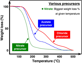
Figure 8. Schematic diagram of thermogravimetric analysis of various precursors. Note: the label of longitudinal coordinates should be 'Weigh (%)' not 'weigh loss (%)'. Reproduced from [43]. © IOP Publishing Ltd. All rights reserved.
Download figure:
Standard image High-resolution imageRim et al reported on aqueous metal complex-based oxide semiconductor films formed with various ligands, such as chloride, acetate, fluoride, and nitrate [46]. They found that nitrate ligand-based indium precursor was easily decomposed at low temperature owing to the replacement of all nitrate ions with water during solvation to form the hexaaqua indium(III) cation ([In(H2O)6]3+). The extracted device parameters of the In2O3 TFTs with different ligands and annealing temperatures are summarized in table 1. This low-temperature formation of hexaaqua complexes was achieved through free carbon residues and a simple dihydroxylation process. Later, Kim et al also reported enhanced electrical stability of IGZO TFTs with this nitrate ligand-based hexaaqua complexes precursor [47]. The relatively good performance of TFTs with the ultrathin solution-processed IGZO channel layer, such as a mobility of 7.73 cm2 V−1 s−1, a subthreshold slope of 0.27 V/dec, an on/off current ratio of 108, and a threshold voltage of 3.10 ± 0.30 V, was attributed to the low bulk resistance, high density of the film, and high interface quality.
Table 1. The extracted device parameters of the In2O3 TFTs with different ligands and annealing temperatures. Reprinted with permission from [46]. Copyright 2015 American Chemical Society.
| Precursor types | Temp. (°C) | μsat (cm2 V–1 s–1) | Ion/off | SS (V/dec) |
|---|---|---|---|---|
| In(C2H3O2)3 | 250 | 0.07 ± 0.02 | ∼105 | 2.05 ± 0.78 |
| InCl3 | 250 | 0.44 ± 0.14 | ∼105 | 0.95 ± 0.37 |
| InF3 | 250 | 1.21 ± 0.10 | ∼106 | 0.92 ± 0.12 |
| In(NO3)3 | 150 | 1.24 ± 0.07 | ∼106 | 0.64 ± 0.01 |
| In(NO3)3 | 200 | 6.27 ± 0.74 | ∼107 | 0.60 ± 0.08 |
| In(NO3)3 | 230 | 14.10 ± 0.97 | ∼108 | 0.55 ± 0.13 |
| In(NO3)3 | 250 | 23.96 ± 1.85 | ∼108 | 0.56 ± 0.22 |
| In(NO3)3a | 250 | 36.31 ± 2.29 | ∼107 | 0.76 ± 0.24 |
The precursor method has an advantage of easy chemical composition control. MO doping can be done easily by adding other metal precursors into the solution, and the ratios of different components can be tuned continuously by changing the ratios of different precursors. However, the processing temperature of the precursor solution method is still high compared with the upper-limit temperature of most of the flexible substrates. Although nitrates have relatively low decomposition temperature compared to acetates or chlorides, the practical annealing temperature is usually greater than 250 °C for MO-TFTs with better performances (see table 1). Therefore, lowering the processing temperature is in particular need for flexible TFTs with cheap plastic substrates. The following section will introduce the solvent engineering method to lower the processing temperature.
2.4. Solvent engineering
Solvents are required for the dissolving precursors in the conventional solution processes. The electrical properties of MO thin films and their TFTs, such as mobility and SS, are strongly affected by the precursor solvents. There are two main kinds of solvents, aqueous and nonaqueous solvents. Nonaqueous solvents, such as 2-methoxyethanol and acetonitrile, have been developed to fabricate solution-processed MO TFTs at relatively high temperature when compared to aqueous route [48–50].
Kim et al reported a systematic investigation of the influence of precursors (i.e. nitrate, acetate, and chloride) and solvents (i.e. 2-methoxyethanol, water, and acetonitrile) on the performance of the solution-processed IZO TFTs [51]. They revealed that the mobility and turn-on voltage (Von) of the devices were dominantly affected by the precursors and solvents, respectively. From their observation, the TFTs fabricated with an acetonitrile solvent had the most positive Von values, while those fabricated with water solvent exhibited the most negative Von value. It was also found that metal vacancies, as deep traps, affected by the solvents, dominantly led to the variation in Von. Their findings are beneficial for investigating and optimizing the fabrication of high-performance solution-processed MO TFTs with various precursors and solvents.
2.4.1. Combustion chemistry
A self-generated combustion chemistry method through adding acetylacetone or urea to 2-methoxyethanol solvent, was proposed and developed by Marks et al in 2011 [52]. The acetylacetone or urea acted as the fuel source, and the metal nitrates precursor acted as the oxidizer. The balanced and highly exothermic oxidizer + fuel reaction for the combustion synthesis of ZnO is shown in the following Equation 1. The heat generated by the reaction assisted the precursor in converting into the corresponding MO at a relatively low temperature. Unlike the conversion of conventional precursors with metal hydroxide and/or alkoxide, which is endothermic, the combustion-based conversion is exothermic. So external energy is not required once the process is ignited. A comparison of the required energy for conversion is shown in figure 9. With this combustion route, the fabricated In2O3 TFT with a low process temperature of 200 °C exhibited a mobility of 1 cm2 V−1 s−1. In 2016, three kinds of environmentally benign carbohydrates, sorbitol, sucrose, and glucose, were also developed to act as highly efficient fuels for self-combustion IGZO thin films [53]. The fabricated IGZO TFTs with SiO2 gate dielectrics exhibited mobility of >8 cm2 V−1 s−1 and dramatically enhanced bias-stress stability.

Figure 9. (a) Depiction of the two different synthetic approaches. (b) Energetics of combustion synthesis-based processes versus conventional processes. Reprinted by permission from Macmillan Publishers Ltd: Nature Materials [52], Copyright 2011.
Download figure:
Standard image High-resolution image
Later, the self-combustion method of a two-component mixture of metal salts whose ligands function both as a fuel and as an oxidizer was proposed and developed by Cho [54]. The IZO precursors consisting of zinc acetylacetonate hydrate (fuel) and indium nitrate hydrate (oxidizer) without any additives released extremely intense exothermic heat, as shown in figure 10. The optimized IZO TFT prepared using an equivalent stoichiometric ratio of fuel and oxidizer with a post-annealing temperature of 350 °C exhibited a field-effect mobility of 13.8 cm2 V−1 s−1 and an on/off current ratio of 1.06 × 10⁸ [54].
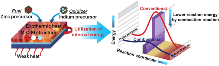
Figure 10. A schematic diagram of MO film synthesis via self-combustion of metal precursors bearing coordinated fuel and oxidizer ligands. Reproduced from [54] with permission of The Royal Society of Chemistry.
Download figure:
Standard image High-resolution imageRecently, Lan et al reported a simple and general chemical route for fabricating In2O3 thin films at a relatively low temperature with a precursor mixture of perchlorate and nitrate [55]. When assisted by nitrate salt, perchlorate salt can be easily decomposed and forms a high-density oxide thin film at a lower temperature. Because ClO4− has the equilateral tetrahedron structure, which is stable, it is difficult to decompose at low temperature. So high temperature (∼320 °C) is usually required to decompose In(ClO4)3, as shown in figure 11 (reaction (2)). After adding nitride into the indium perchlorate, the oxygen radicals (with strong oxidability) released from NO3− at the beginning assisted in the decomposition of ClO4−, as shown in figure 11(a) (reaction (3)). Unlike ClO4−, all intermediate compositions of ClO3−, ClO2−, and ClO− generated from the ClO4− decomposition were unstable and easily decomposed, generating more oxygen radicals, which in turn assisted in the whole decomposition of more ClO4−. The comparison of the transfer characteristics of In2O3 TFTs device fabricated with perchlorate, nitrate, and their precursor mixture under the same annealing temperature is shown in figure 11(b). It can be seen that TFT fabricated with mixture precursors of perchlorate and nitrate showed the highest on-current, which indicates the highest mobility (∼14.5 cm2 V−1 s−1).

Figure 11. (a) Schematic diagram of the reaction mechanism of the precursor mixture. (b) Transfer characteristic curves of the In2O3–TFT devices made of In(NO3)3, In(ClO4)3, and their 1:1 precursor mixtures annealed at 250 °C. Reproduced from [55] with permission of The Royal Society of Chemistry.
Download figure:
Standard image High-resolution image2.4.2. Aqueous route
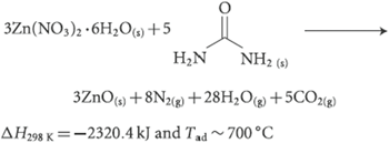
Another method for lowering the annealing temperature is the aqueous route, which is based on precursors' water solution without any fuel additives. This environmentally friendly and carbon-free route was first developed and demonstrated by Keszler et al in 2008 [56]. In this methods, an aqueous Zn(OH)x(NH3)y(2−x)+ solution formed by dissolving Zn(NO3)2 · 6H2O in distilled H2O rapidly decomposed to polycrystalline wurtzite ZnO at low temperature (<150 °C), while it was stable at room temperature.
In 2013, Bae et al reported flexible and transparent MO TFTs via the aqueous route on plastic substrates at a low process temperature (<200 °C) [57]. When the indium precursor (In(NO3)3) was dissolved in water, the ionized indium cation (In3+) was solvated by the neighboring water molecules. The formation of [In(OH2)6]3+ was confirmed by Raman spectrum analysis, as shown in figure 12(a). The peak centered at 485 cm−1 belongs to the totally symmetric In-O stretching vibrations, which provides evidence of the expected structure. As illustrated in figure 12(b), the thermogravimetric analysis for different precursor solutions (aqueous solution and 2-methoxyethanol solution) implies that the thermal decomposition temperature is substantially decreased by the aqueous route. The resulting transparent TFT on flexible polythylene naphtalate (PEN) substrate showed good negative and positive bias stress stability, and good electrical performance, including a field-effect mobility of 3.14 cm2 V−1 s−1, a sub-threshold slope of 158 mV/decade, and an on/off current ratio of 109.
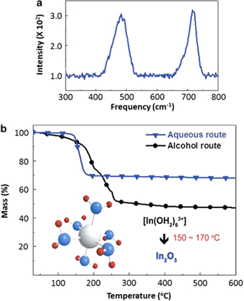
Figure 12. Structure and thermal analysis of the aqueous- and conventional 2-methoxyethanol-based solutions. (a) Raman (300–800 cm−1) spectrum of the aqueous solution. (b) Thermogravimetric analysis traces of the aqueous- and 2-methoxyethanol-based solutions used for the deposition of In2O3 thin films. The chemical structure in the inset represents the proposed indium complex in the aqueous solution. [57] 2013 Springer Nature and Copyright Clearance Cente. With permission of Springer. CC-BY 3.0.
Download figure:
Standard image High-resolution imageIn 2015, Rim et al gave a systematic investigation of In2O3 thin film using various metal salt precursors (chloride, acetate, fluoride, and nitrate) through this environmental friendly aqueous route [46]. The formation of hexaaqua indium (III) cation In-(H2O)6]3+ in the solution was found to be the key factor for lowering the decomposition temperature. It was found that the highest quality MO (In2O3, Al2O3) thin film was achieved from the nitrate-based aqueous precursor at low temperature. The fabricated In2O3 TFT exhibited h a mobility of as high as 25 cm2 V−1 s−1. Later, Kim et al investigated the effect of a-IGZO thickness on the properties of the corresponding TFTs [44]. They reported that the TFT with an ultrathin a-IGZO channel layer showed a saturation mobility of 7.73 ± 0.44 cm2 V−1 s−1, a SS of 0.27 V/dec, an on/off ratio of ∼108, a threshold voltage of 3.10 ± 0.30 V, and good positive and negative bias stress stability, which are attributed to the low bulk resistance, high film density, and good a-IGZO/SiO2 interface quality.
In 2017, Lan et al also reported solution-processed scandium (Sc)-substituted indium oxide (ScxIn1−xO3) thin films with the environmentally friendly aqueous route [58]. The precursor was prepared by dissolving indium nitrate hydrate [In(NO3)3·xH2O] and scandium nitrate hydrate [Sc(NO3)3·xH2O] in deionized (DI) water. The optimized ScxIn1−xO3 TFTs showed a field-effect mobility of 6.4 cm2 V−1 s−1, and improved electrical stability under gate bias stress owing to the reducing of the oxygen vacancies after incorporated with Sc.
In the same year, fully solution-processed MO TFTs through this environmental friendly aqueous route were demonstrated by Xu et al [59]. Various MOs, such as In2O3 or IZO serving as the channel materials, were synthesized and systematically studied using a variety of characterization methods. They revealed that water-based precursors underwent decomposition of the nitrate complex and conversion of metal hydroxides to form a high quality MO framework. The fabricated In2O TFT with an annealing temperature of 250 °C showed a field-effect mobility of 36.69 cm2 V−1 s−1 and an operation voltage of 4 V. In the same year, Subramanian et al reported all-aqueous route In2O3 TFTs with Al2O3 gate dielectric and Cd-Al-O source/drain electrodes using an inkjet-printed coating method. The TFT exhibited high electrical performance including a mobility of 19 cm2 V−1 s−1, a subthreshold slope of 150 mV/dec, and an on/off current ratio of 107 [60].
Because of the non-toxic, environmental friendly, and low-decomposition-temperature properties of the aqueous solvent route, numerous studies on the various compositions of the MO, including the semiconductor materials (e.g. InNdO [61], InAlO [62], IZO:F [63]) and dielectric materials (e.g. ZrO2 [64], HfO2: Y [65], ScOx [66]) were carried out recently.
The combustion method may induce new impurities because of the fuel additive. Moreover, the combustion process in the film can cause poor film quality. In contrary, the aqueous solvent route is mild has fewer impurities, leading to higher film quality. However, the viscosities of the aqueous solution is usually too low for inkjet printing (see section 3.2). Despite there are some reports on inkjet-printed MO-TFTs with aqueous solvent, the controllability and reproducibility are still questioned.
2.5. Metal oxide composition
As mentioned above, the binary MO semiconductors are not good candidates for TFTs. Instead, multicomponent MO semiconductors are preferred for their better TFT performance. The roles of the constituent elements in the MO semiconductors were systematically investigated by Hosono et al [4]. Indium, gallium, zinc and tin are the major elements for achieving high quality MO semiconductors, because of their unoccupied s orbitals which form the electron transport paths in the MO systems. Generally, IZO has higher mobility than IGZO. However, it is difficult for IZO to control the carrier concentration at a low level, which is important for TFTs to operate at enhanced mode (Vth > 0 V). Typically, in IGZO, an increase in In ratio is related to a decrease in film resistivity, because a high In ratio leads to a large number of oxygen vacancies. Therefore, a greater percentage of In in IGZO results in a negative shift of Vth, and an increase of the off current (Ioff). In contrast, Ga serves as the suppressor and the stabilizer to suppress the generation of oxygen vacancies and decreases the free electron concentration, because the Ga–O bonds are much stronger than In–O and Zn–O bonds. Numerous studies have focused on finding other metal atoms to replace Ga to enhance the stress stability. Low standard electrode potential (SEP), large bandgap, and low electronegativity are the three main considerations for the alternative atoms [36].
SEP is a parameter responsible for the degree of metal oxidization. Hf is supposed to be an effective atom to decrease oxygen vacancies due to its lower SEP (−1.7 V) as compared to that of Ga (−0.52 V). Jeong et al studied the effects of adding Hf into IZO (named HIZO) with various Hf ratios (0–10 at%) [67]. It was concluded that HIZO TFT with 10 at% Hf exhibited a linear mobility of 1.94 cm2 V−1 s−1, an on/off current ratio of 3.64 × 10⁶, and a SS of 0.58 V/decade. Compared to IGZO TFTs, HIZO TFTs had lower Ioff, which indicates that the free carriers can be suppressed by Hf effectively.
MOs with a large bandgap can make the donor-related levels move toward deep levels, and decrease carrier concentration. MgO is believed to be a good carrier suppressor due to the low SEP (−2.37 V) and large bandgap (∼7.9 eV). The characteristics of Mg–InZnO with various Mg concentrations fabricated by a solution process with 2-methoxyethanol solvent was studied by Kim et al [68]. As the Mg concentration increased, the optical bandgap increased, which caused an increase of the activation energy for donor-related shallow defect states. High-performance and enhanced-stability MgInZnO TFTs were achieved with the optimized Mg concentration of [Mg]/([In] + [Zn]) = 0.2. The shift of the threshold voltage was about −2.9 V under negative bias temperature stress (NBTS) (VDS = 10 V, VGS = −20 V, T = 60 °C, and stress time = 3 h). This degradation can be interpreted by a charge-trapping model, which means that electrons are trapped at the mid-gap and holes in the valence band drift to the channel/insulator interface and then are trapped. In addition to Mg–InZnO, Mg–ZnO, Mg–ZnSnO, Mg–InGaZnO, and MgInO semiconductors have also been investigated and studied [69–73].
In 2017, Lan et al demonstrated high-mobility, good-stability Nd-incorporated In2O3 (InNdO) TFTs through an environmentally friendly nitrate-based aqueous route [61]. It was found that Nd in the InNdO is a superior oxygen binder to suppress the formation of oxygen vacancies and control the carrier concentration. Moreover, Nd3+ ions incorporated in the In2O3 will not generate excess carriers, since Nd3+ ions have the same valence as In3+ ions. The patterning of the InNdO active layer was realized by a surface-selective coating method associated with a long-term UV irradiation process to change the surface wettability. The post-annealing process was carried out at a temperature of 350 °C for 1 h in ambient condition to remove the solvent and residues and to form MO lattice. The optimized InNdO TFT with an Nd:In ratio of 0.02:1 exhibited a mobility of 15.6 cm2 V−1 s−1, a turn-on voltage of −3.6 V, a SS of 0.34 V/dec, and relatively good bias-stress stability.
In 2018, Marks et al reported nitrate-complex solution-processed MO TFTs by doping both the In2O3 semiconductor and Al2O3 gate dielectric with boron (named IBO and ABO, respectively) [48]. They revealed that B doping frustrates In2O3 crystallization while suppressing defects responsible for electron trapping and oxygen vacancies. IBO thin films were prepared with acetylacetone-based combustion solutions constituted of In(NO3)3·xH2O, H3BO3, AcAcH, NH4OH, and 2-methoxyethanol, while ABO thin film was synthesized from the precursor solutions with Al(NO3)3, H3BO3, and 2-methoxyethanol. The schematic fabrication processes of the IBO films and their TFTs are illustrated in figure 13(a). To figure out the effect of B doping on the structure and electronic properties of IBO, ab initio MD simulations and DFT calculations were performed. It was found that the lower coordination of In atoms associated with the presence of B combined with the lack of nonshared In pairs with comparable energies, favors the formation of deep, strongly localized defects, as depicted in figure 13(b). The optimized solution-processed TFT based on IBO channels with 6 at% B and ABO dielectrics with 10 at% B showed a mobility of 11 cm2 V−1 s−1, an on/off current ratio larger than 105, a threshold voltages of 0.6 V, and high bias-stress stability.
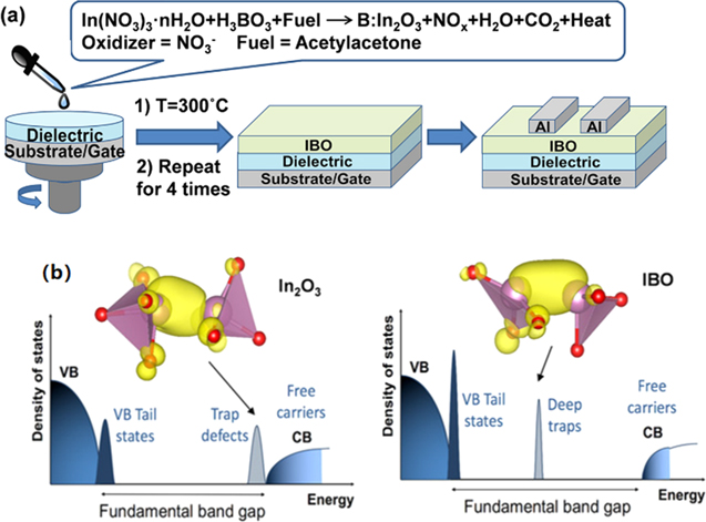
Figure 13. (a) Schematic of the IBO film and TFTs fabrication process, and (b) schematic of density of states and the calculated charge density for the electron trap defect state in In2O3 and IBO thin film. Reprinted with permission from [48]. Copyright 2018 American Chemical Society.
Download figure:
Standard image High-resolution imageIn addition to IBO, boron-doped IZO (BIZO) TFTs were fabricated by Li et al [74]. The BIZO TFT with a 5 mol% B exhibited good electrical performance with a mobility of 10.15 cm2 V−1 s−1, a threshold voltage of 3.29 V, a subthreshold swing of 0.35 V/decade, and an on/off current ratio of 108. The shift of the threshold voltage was only −1.59 V under negative bias illuminant stress (NBIS, a 1000 Lux white light source, −7 V effective negative bias voltage, and 1 h duration). The electrical performances of TFTs with different channel materials are summarized in table 2.
Table 2. The electrical performance of TFTs devices with different metal compositions.
| Channel/GI | T (°C) | Precursor | Solvent | μ (cm2 V−1 s−1) | SS (V/Dec) | References |
|---|---|---|---|---|---|---|
| HfInZnO/SiNx | 500 | Indium nitrate zinc acetate hafnium chloride | 2-methoxyethanol | 1.94 | 0.58 | [67] |
| LiZnO/SiO2 | 500 | Acetate | 2-methoxyethanol | 5.18 | 1.2 | [75] |
| LiInZnO/ZrO2 | 300 | Indium nitrate zinc acetylacetonate lithium nitrate | 2-methoxyethanol | 12 | — | [76] |
| LaInO/ZrO2 | 500 | Nitrate | 2-ethoxyethanol acetylacetone | 32.7 | 0.12 | [50] |
| MgInO/SiO2 | 500 | Indium nitrate magnesium acetate | 2-methoxyethanol acetylacetone | 13.77 | 0.85 | [71] |
| InBO/AlBO | 300 | Nitrate | 2-ethoxyethanol acetylacetone | 11.3 | 0.17 | [48] |
| BInZnO/SiO2 | 500 | Indium nitrate zinc acetate | 2-methoxyethanol | 10.15 | 0.35 | [74] |
| WInZnO/SiO2 | — | Indium nitrate zinc acetate tungsten chloride | 2-methoxyethanol | 24.5 | 0.3 | [49] |
| InGdO/AlOx | 250 | Nitrate | Acetonitrile ethylene glycol | 9.74 | 0.079 | [77] |
| NbZnSnO:N/SiO2 | 430 | Niobium chloride zinc nitrate tin chloride | Ethylene glycol monomethyl ether MEA | 7.4 | 0.3 | [78] |
| SnGaO/SiO2 | 350 | Gallium nitrate tin chloride | 2-methoxyethanol acetylacetone | 4 | 0.6 | [79] |
| ZnSnO/Al2O3 | 400 | Zinc nitrate tin chloride | 2-methoxyethanol | 3.05 | — | [80, 81] |
| GaCdO/SiO2 | 450 | Nitrate | 2-methoxyethanol | 5.1 | 0.83 | [82] |
| InGaCdO/SiO2 | 400 | Nitrate | 2-methoxyethanol | 10.1 | — | [83] |
2.6. Novel structures for channel
Compared to vacuum-processed MO-TFTs, solution-processed MO-TFTs have lower mobility due to the relatively poor film quality and the impurities induced by the solvents or precursors. Thus, some research teams are trying to design novel structures for solution-processed MO-TFTs to enhance the mobility. One of the effective way is employing heterojunction (HJ) channels. The conduction offset at the HJ interface would induce high density of electrons, leading to quasi 2D electron gas-like transport. According to the percolation model, the mobility of MO semiconductors increases with increasing electron density.
In 2015, Anthopoulos et al reported high electron mobility solution-processed MO TFTs utilizing HJ and quasi-superlattices (QSLs) structures, which were composed of alternating layers of In2O3, Ga2O3, and ZnO deposited by sequential spin casting of corresponding precursors in air at quite low temperatures (180 °C–200 °C) [84]. Cross-sectional schematics of the proposed HJ and QSL-based TFTs are illustrated in figure 14(a).
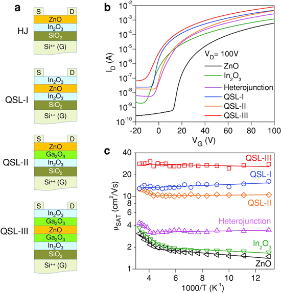
Figure 14. Electrical characterization of TFTs. (a) Schematics of the HJ and QSL‐based MO TFTs. (b) Transfer characteristics of the TFTs with different active channel layers. (c) Arrhenius plots of the temperature dependence of the saturation mobility with different active channel layers. [84] John Wiley & Sons. © 2015 WILEY‐VCH Verlag GmbH & Co. KGaA, Weinheim.
Download figure:
Standard image High-resolution imageThe optimized prototype QSLTFTs exhibited band-like transport with electron mobilities approximately a tenfold greater (25–45 cm2 V−1 s−1) than single oxide devices (typically 2–5 cm2 V−1 s−1), as shown in figures 14(b) and (c). Based on temperature-dependent electron transport and capacitance-voltage measurements, it is argued that the enhanced performance arises from the presence of quasi 2D electron gas-like systems formed at the carefully engineered oxide heterointerfaces (see figure 15).
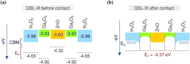
Figure 15. Energy levels of the individual oxides used in QSL‐III before and after contact. [84] John Wiley & Sons. © 2015 WILEY‐VCH Verlag GmbH & Co. KGaA, Weinheim.
Download figure:
Standard image High-resolution imageIn 2017, the same team also developed In2O3/Li-doped ZnO HJ TFTs with a post-annealing temperature of 200 °C [85]. Li is an n-type dopant for ZnO, which can tune the Fermi energy (EF) of ZnO accurately. With the large EF offset (ΔEF) between In2O3 and Li-doped ZnO, large band bending took place at the HJ interface, resulting in the accumulation of high density of electrons in the vicinity of the HJ. They also found that the charge transport in the In2O3/Li-doped ZnO HJ TFTs follows percolation model. As a result, the mobility increases greatly.
A low-temperature spray-processed TFT based on a ZnO/Ga2O3 heterostructure was also reported by Subramanian et al in 2017 [86]. Both of the Hall mobility and field-effect mobility were greatly improved due to directional electron transfer from Ga2O3 to ZnO, which was similar to their previous investigation in a ZnO/ZrO2 system [87]. Their observation was supported by work function differences achieved for the individual films as a function of processing temperature.
Additionally, a corrugated HJ channel structure was proposed and developed by Park et al in 2018 to achieve high mobility, low leakage current, and stable MO TFTs [88]. The corrugated HJ channel, consisting of alternating thin and thick ITZO/IGZO film regions, changed the accumulated electron concentration effectively via charge modulation at the vertical regions of the HJ in the on or off state of the device. The fabrication process and cross-sectional schematic of the proposed corrugated ITZO/IGZO heterostructure is illustrated in figure 16.
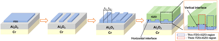
Figure 16. The 'corrugated' ITZO/IGZO heterostructure fabrication scheme and the proposed TFTs. [88] John Wiley & Sons. © 2018 WILEY‐VCH Verlag GmbH & Co. KGaA, Weinheim.
Download figure:
Standard image High-resolution imageAs shown in figures 17(a) and (b), the TCAD simulation results show that the corrugated structure enables the formation of an extremely high carrier concentration in the vertical interface regions, which can migrate to the bottom channel of the ITZO layer upon application of positive gate bias. On the other hand, as shown in figures 15(c) and (d), in the off state, the electron concentration of the confined region #2 is much lower than that of the confined region #1 if negative gate bias is applied, which means that the overall resistivity of the current path increase, resulting in reduction of the off-state current.

Figure 17. TCAD simulation of corrugated heterojunction ITZO/IGZO TFTs. (a) Contour of current density in the on-state (VG = 15 V and VD = 0.1 V) with highlighted current enhancement regions in the enlarged inset picture. (b) Current density profiles in corrugated heterojunction ITZO/IGZO channel (along the cut-line) and planar ITZO/IGZO channels (ITZO thickness of 5 and 10 nm). (c) Contour of current density for off-state (VG = −15 and VD = 0.1 V). (d) Electron concentration as a function of the gate voltage sweep (−15 to 15 V) in the indicated thick- (region #1) and thin-ITZO/ IGZO heterointerface (region #2). [88] John Wiley & Sons. © 2018 WILEY‐VCH Verlag GmbH & Co. KGaA, Weinheim.
Download figure:
Standard image High-resolution image2.7. Post-treatment process
Generally, post-treatment processes, such as annealing, UV treatment, and plasma treatment are required for removing organic residues and attaining high quality M–O–M frameworks. Higher annealing temperature can usually result in high film quality and high TFT performance. However, high-temperature process is not compatible with most of the flexible substrates, limiting its applications in flexible electronic devices. To lower the annealing temperature, numerous novel post-treatment methods for solution-processed MO TFTs have been proposed.
Park et al developed a deep-ultraviolet (DUV) photochemical activation annealing method for solution-processed MO TFTs [89]. The light source of the DUV treatment system is a low-pressure mercury lamp with two main emission peaks at 253.7 nm (90%) and 184.9 nm (10%). The MO TFTs on polymer substrates with DUV treatment exhibited good electrical performance. Later, Park et al reported a profound study of the mechanism of the DUV activation in various sol–gel MO films [90]. DUV irradiation can cause significant condensation, densification, and impurity decomposition at low temperature through photochemical activation, which is possible within 5 min via in situ radical-mediated reactions. This rapid low-temperature photochemical activation process of various sol–gel MO films is depicted in figure 18 [90].
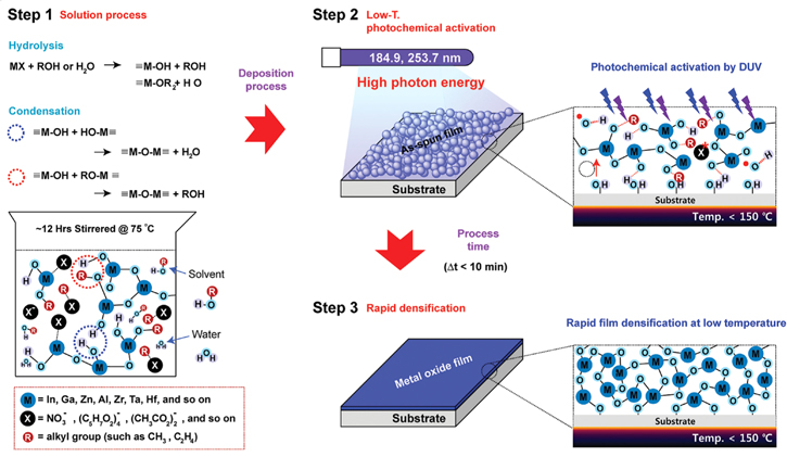
Figure 18. Schematic illustration of the rapid low-temperature photoactivation of various sol–gel MO films. [90] John Wiley & Sons. © 2015 WILEY‐VCH Verlag GmbH & Co. KGaA, Weinheim.
Download figure:
Standard image High-resolution imageLeppaniemi et al proposed a combined treatment of thermal annealing and far-ultraviolet (FUV) exposure to convert inkjet-printed precursor films to high quality In2O3 films on flexible substrates with process temperature of 150 °C [91]. The fabricated In2O3 TFTs exhibited saturation mobility of 4.3 cm2 V−1 s−1 and ∼1 cm2 V−1 s−1 on rigid Si/SiO2 and flexible plastic PEN substrates, respectively. From the analysis of FTIR and x-ray measurements, the authors found that the average density of the resulting In2O3 films increased after FUV annealed.
Lee et al proposed a UV-O3 treatment method on the selective layer during multiple active layer formation [92]. The location and concentration of oxygen vacancies could be well controlled by the UV-O3 treatment, bringing about improved TFT performance.
Although visible lasers cannot provide sufficient energy to convert precursors to the complete M–O–M framework due to the low absorption of visible rays in the wide-bandgap MO semiconductor films, a visible blue laser is efficient for assisting in lowering the annealing temperature of the combustion process [93]. In this method, urea (CH4N2O) was added to the In2O3 precursor as a fuel and a stable continuous-wave laser with a wavelength of 450 nm was utilized to ignite this combustion process. The In2O3 TFT fabricated based on laser annealing exhibited a mobility of 2.76 cm2 V−1 s−1 and a SS of 107.5 mV/dec.
Cho et al employed microwave irradiation (MWI) to treat solution-processed ZTO films with a highest process temperature of 180 °C [94]. MWI is efficient for transferring energy to a sample, because it can generate heat by molecular vibrations. The proposed ZTO TFTs with the MWI method showed good electrical characteristics, including an on/off current ratio of 1.7 × 10⁸, a small hysteresis of 0.96 V, a SS of 194 mV/dec, and a field-effect mobility of 13.6 cm2 V−1 s−1.
A rapid thermal annealing (RTA) process was employed for the decomposition and condensation of nitrate-based solution processed a-IGZO thin films by Lee et al in 2018 [95]. Sol–gel reactions with the RTA treatment can happen at a low temperature of 180 °C. The authors revealed that the RTA process generates both photonic and thermal energies, and thus effectively boost sol–gel reactions at low temperature.
The effect of ambient conditions (e.g. He, Ar, and N2) during annealing on the electrical characteristics of a-IGZO TFTs was investigated by Jeong et al [96]. They revealed that the He-annealed TFTs with a relatively short annealing time of 30 min exhibited comparable performance compared to the N2-annealed ones due to the high thermal speed of the He atoms.
In 2018, atmospheric-pressure plasma (APP) treatment for solution-processed InOx TFTs was developed by Kim et al, as shown in figure 19 [97]. The oxygen vacancies and carrier concentration of solution-processed InOx thin film can be well controlled through this APP treatment. The fabricated InOx TFTs with low temperature (∼250 °C) annealing and APP treatment exhibited a high mobility of 20 cm2 V−1s−1, and an on/off current ratio of 106.
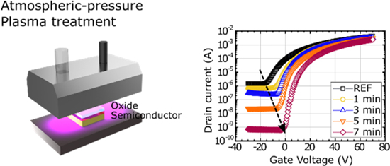
Figure 19. The schematic of plasma treatment in air, and the transfer characteristics of the InOx TFTs with different APP treatment times. Reprinted with permission from [97]. Copyright 2018 American Chemical Society.
Download figure:
Standard image High-resolution imageThe effect of N2O plasma treatment on the performance of a-InMgZnO TFTs was also investigated by Yu et al in 2018 [73]. The field-effect mobility of the optimized devices was shown to be five times larger than that of devices without N2O plasma treatment.
The DUV, FUV and UV + O3 treatment methods are based on the UV-light-assisting precursor decomposition. As know, UV light can be absorbed by MO semiconductors, and the energy of the UV photons is high, so compared to visible laser annealing, the UV (especially DUV/FUV) treatment is more effective for helping MO semiconductor precursors decompose. However, UV light can be absorbed by most of the substrates (e.g. PEN), so the heating of the substrate by UV light cannot be neglected. Compared to UV, microwave cannot be absorbed by most of the substrates, so the substrate heating during MWI can almost be neglected if not consider heat conducting.
3. Deposition methods for solution-processed MO films
After MO precursor solutions (inks) are prepared, they should be converted into patterned thin films on the substrates. Spin coating is the most common method, but it cannot pattern the coated thin-films. This section focuses on the deposition (patterning) techniques for solution-processed MO films, and the advantages and/or disadvantages of different techniques are discussed.
3.1. Direct photopatterning techniques
The direct photopatterning technique is patterning the MO precursor film using UV light irradiation without photoresist, as shown in figure 20 [98]. When the MO precursor film is irradiated by UV light, the sol–gel process takes place, converting the precursor film into oxides/hydroxide, making it insoluble in the solvent. Thus, after immersed in solvents, the UV-irradiated parts of the MO precursor film remain, while the un-irradiated parts are dissolved and removed. Compared to the conventional photolithography technique, which is complicated and time-consuming, the direct photopatterning technique has the advantages of simplicity, low cost, and short process time, see figure 20 [98].
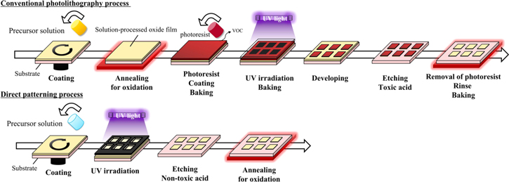
Figure 20. Comparison of process flow for MO film fabrication using a conventional photolithography process versus direct patterning process. [98] 2018 Springer Nature and Copyright Clearance Cente. With permission of Springer. CC-BY 4.0.
Download figure:
Standard image High-resolution imageSelf-patterned solution-processed MO TFTs using a photosensitive sol–gel route were proposed by Kim et al in 2014 [99]. The photosensitive sol-gels were obtained by adding β-diketone compounds, such as benzoylacetone and acetylacetone, acting as the photo-activator, to the sol–gel solution. After spin-coating and pre-baking, the ZTO gel films were hard-contacted to a photomask to achieve high-resolution patterns and then irradiated using a UV lamp with wavelength of 365 nm and power density of 48 mW cm−2 for 10 min. The UV-irradiated parts of the ZTO gel films remained, while the un-irradiated parts dissolved into 2-ME solution during the leaching process. However, the fabricated fully self-patterned ZTO TFT with high annealing temperature of 500 °C exhibited a low mobility of 0.03 cm2 V−1s−1. Another simple method using metal acetylacetonates was also developed for the direct photopatterning of sol–gel solutions [100]. These admixtures are beneficial for transferring UV-energy to the precursor molecules, prompting a smooth decomposition process.
In 2016, a photocurable polymer precursor, zinc acrylate (ZDA), was employed for the direct photopatterning of ZnO channel layer for TFTs [101]. After UV-irradiated (254 nm), the ZDA thin films became insoluble in isopropyl alcohol (IPA), because of the photo-crosslinking effect of the acrylate moiety. The process procedure is illustrated in figure 21. The ZnO TFT with an ion-gel gate dielectric exhibited a mobility of 7.14 cm2 V−1s−1, an on/off ratio of 105, and no obvious hysteresis. Combined with the conventional pentacene TFTs, organic/inorganic hybrid complementary inverters with low operation voltages was demonstrated, as shown in figure 21.

Figure 21. Schematic illustration of the experimental procedure of the photopatterning ZnO thin film, the optical microscopy images of pZA film, and the performance of the complementary inverter (VTCs and DC voltage gain with various VDD values). Reprinted with permission from [101]. Copyright 2016 American Chemical Society.
Download figure:
Standard image High-resolution imageTo lower the post-annealing temperature of the photopatterned MO thin films, air-, visible light-, and solution-stable molecular precursors were developed for UV-photopatternable sol–gel thin films by Schneider et al in 2018 [102]. Indium, zinc, and tin with methoxyiminopropionato ligands (metal oximates, In(C4H6NO3)3, Zn(C4H6NO3)2, and Sn(C4H6NO3)2) were used as precursors for IZO and ZTO films. The decomposition of the metal complex formed gaseous molecules (CO2, CO, CH3CN, H2O), which left the film under modest conditions, resulting in a high quality thin film without by-product contamination. The part of the thin film without a 10 min UV-irradiation process remained soluble and can be dissolved completely by solvent, while precursor decomposition and polymerization occur in the other part of thin film with 10 min UV irradiation (peak λ = 254 nm, 90%; 186 nm, 10%). The fabricated direct photopatterning IZO TFT with a post-annealing temperature of 350 °C showed a saturation mobility of 7.8 cm2 V−1 s−1 and an on/off current ratio of 3.5 × 10⁸. The enhanced performance of the direct photopatterning IZO TFTs is attributed to the increase of the metal-oxygen bonds and decrease of hydroxyl groups.
A direct light-patterning technique was also employed for solution-processed a-IGZO TFTs by Lee et al in 2018 [103]. Based on the proposed a-IGZO TFTs, a novel operational amplifier (op-amp) fabricated on a glass substrate exhibited a total gain of 24.6 dB, a cutoff frequency of 0.47 kHz, and a unit-gain frequency of 2.0 kHz at a supply voltage of ±15 V.
All the above mentioned precursors were prepared with carbon-based materials, such as organic solvents, additives, and ligands in metal salts, which are not environmentally friendly. In 2016, Lan et al proposed a simple and 'green' direct photopatterning method using an aqueous precursor consisting of chloride ligand-based indium(III) and DI water without any additives [104]. The as-spin-coated precursor films could be facilely patterned using the 'green' patterning method, which required only ultraviolet (UV) irradiation and DI water washing. It was found that UV irradiation and water treatment not only helped to transform In-Cl into In-OH, but also helped to remove the Cl-related impurities. It led to the activation of InOx films at temperatures as low as 180 °C. The mobility of InOx TFTs with 'green' patterning was improved by more than 1 order compared to that without patterning at an annealing temperature of 280 °C. In addition, flexible InOx TFTs on polyimide (PI) substrates were demonstrated. They showed only a little degradation in the subthreshold region of the transfer curve even at a bending curvature (R) of 5 mm.
Later in 2018, a carbon-free aqueous route a-IGZO thin film and the related TFTs were demonstrated by Miyakawa et al through a simple and reliable direct photopatterning method. It was realized by selective photoreaction of water molecules under UV irradiation and by an environmentally friendly chemical etching process using a non-toxic acid, as shown in figure 22 [98]. The precursor solution was formed by dissolving nitrate-based metal complex in DI water. The photoreaction process was performed using a deep-UV irradiation system (185 nm (10%) and 254 nm (90%)) for 10 min, and the post-annealing process was performed at a temperature of 350 °C for 1 h in air. The photochemical reaction of water molecules immediately occurred in the aqueous precursor based on free-radical reactions caused by UV irradiation. A non-toxic dilute organic acid, citric acid, was used for etching solvent. The fabricated IGZO TFTs with SiO2 dielectrics exhibited average mobility of 4.3 cm2 V−1 s−1 and good stability under positive or negative bias stresses.
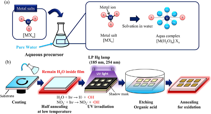
Figure 22. (a) Aqua complexes [M(H2O)m]Xn formed by solvation with water molecules in the aqueous precursor. (b) Schematic illustration of the direct photoreactive patterning method. [98] 2018 Springer Nature and Copyright Clearance Cente. With permission of Springer. CC-BY 4.0.
Download figure:
Standard image High-resolution imageA femtosecond (fs) laser was employed by Chen et al to pattern and anneal the synthesized IZO thin films for TFTs [105]. Uniform patterned arrays with sharp edges and a feature size (32 μm) were obtained using this fs-laser ablation. Additionally, fs-laser annealing reduced the thermal budget and realized sufficient dehydroxylation reaction for OH-related species, resulting in enhanced mobility.
Because the patterning resolution of the direct photopatterning technique depends on the resolution of the photo mask, high-resolution patterning is possible by using the direct photopatterning technique, which can even be comparable with the conventional photolithography technique. But it is not a drop-on-demand (DOD) method, so the material waste is unavoidable. What is more, it requires photo masks and the UV irradiation systems, which will increase the cost.
3.2. Printing technique
As compared to the other thin film coating methods, the printing technique offers several advantages including direct writing of materials, reduction of chemical waste, and reproducibility at high-resolution scale. There are several printing techniques including conventional contact printing [106, 107], aerosol jet printing [108, 109], electrohydrodynamic (EHD) jet printing [110, 111], inkjet printing [112, 113], and nano-imprint lithography (NIL) etc. The conventional contact printing techniques, which include gravure, flexographic, offset, and screen printing, transfer the printable functional inks onto the contact zone to form predesigned patterns on the substrates. They have a long-lasting history and will remain important for a wide application, because they are suitable for roll-to-roll process (R2R, see figure 23) [114]. Gravure printing has attracted much attention because of the potential for low manufacturing costs, as well as large-area and high-throughput fabrication. Kim et al investigated the effect of the printing parameters (such as speed and force) on the characteristics of a-IGZO TFTs [115]. As the gravure printing force increased, the thickness of the printed film decreased and the refractive index increased. With the optimization of the print speed and force, the fabricated bottom-gate a-IGZO TFT showed a field-effect mobility of 0.81 cm2 V−1 s−1 and an on/off current ratio of 1.36 × 10⁶. Flexographic printing is designed for thin, uniform layers providing a better pattern integrity and sharper pattern edges than gravure printing [116]. Offset printing combines the high resolution and layer quality of gravure printing with a comparatively simple and inexpensive printing plate fabrication, making it attractive for the fabrication of source and drain electrodes [117]. Screen printing is an inexpensive, large-area printing technique with good control over the deposition area. It is an important requisite for fabricating a device that is integrated onto a substrate containing other electronic devices [118]. Although the conventional contact printing is attracted for its high-efficiency, large-area capability, the limited resolution and control over the layer thickness and homogeneity restrict the applicability for the high-throughput, large-area fabrication of high-resolution flexible-device components such as small-channeled, flexible TFTs. Furthermore, the contact printing is more suitable for high-viscosity inks, so the viscosity of the MO precursor solution should be increased by adding high-viscosity additives.
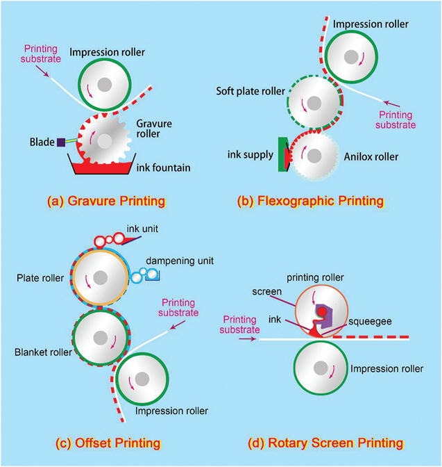
Figure 23. Schematic illustration of conventional R2R patterning technologies and the key physical processes involved in aerosol jet printing. Reproduced from [114] with permission of The Royal Society of Chemistry.
Download figure:
Standard image High-resolution imageAerosol jet printing is a new printing technology proposed in recent years, which includes the preparation of an ink aerosol followed by spraying the aerosol onto the surface of the substrates. The viscosity requirement for the inks is very low, and the resolution is quite good. The schematic illustration of aerosol jet printing, as well as the EHD printing and inkjet printing are shown in figure 24. A survey of the critical line width of these typical printing techniques as utilized to print on various substrates have been made in elsewhere [107].
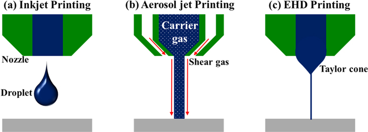
Figure 24. Schematic illustration of (a) conventional inkjet printing, (b) aerosol jet printing, and (c) electrohydrodynamic jet printing.
Download figure:
Standard image High-resolution imageEHD printing is an emerging printing technique that offers high-resolution printing. Because EHD can produce a jet or droplet that is much (up to a few orders of magnitude) smaller than the nozzle diameter [119], large nozzles can be used in EHD printing to produce micro-scale lines. So EHD printing can evade the dilemma of printing resolution and nozzle clogging. In 2016, Park et al reported high resolution In2O3 TFTs with a minimum line width of 2 μm using EHD printing technology [111]. The resulting In2O3 TFT exhibited a mobility of as high as 230 cm2 V−1 s−1, a SS of 0.2 V/dec, and good stress stability. Although the resolution of EHD printing is high, it is not easy to print uniform films stably, especially for those with low conductivity.
Inkjet printing is one of the most promising alternatives to vacuum and photolithographic processes. Inkjet printer is a DOD printer that only ejects drops of inks as the digital signal asks for it. It enables direct patterning of thin-film: predetermined area deposition with computer control. Thin films with different patterns can be directly deposited on the substrate by inkjet printing, and the patterns can be easily designed and changed by a computer. Inkjet printing deposition depends on the formation of droplets at or near a nozzle aperture, followed by noncontact deposition onto a substrate with high spatial control. For a typical inkjet printing system, the reciprocal of the Ohnesorge number (Z) is a significant parameter in evaluating the inkjet's ability to generate a droplet. The Z value is a dimensionless number related to the viscosity and surface tension of the printing inks [120, 121].

where μ, ρ and σ are the viscosity, density and surface tension of the ink, respectively; L is the diameter of the droplets, and Re and We are the Reynolds number and Weber number, respectively. When 2 < Z < 4, stable inkjet printing without satellite droplets can be achieved, because the satellite droplets run after the primary droplets and catch them [114].
The first report of inkjet-printed MO TFTs was given by Chang et al in 2007 [122]. The ink solution was composed of ZnCl2 and InCl3 (1:1 molar ratio) in acetonitrile solvent. The TFT exhibited a mobility of 16 cm2 V−1 s−1.
Hersam et al developed a complementary circuit composed of inkjet-printed SWCNT TFTs (acting as p-channel) and amorphous ZTO TFTs (acting as n-channel) [123, 124]. The schematic structure of the proposed complementary inverter is shown in figure 25 [123]. The post-annealing process was carried out on a hot plate at a temperature of 500 °C for 1 h in air. The inkjet-printed ZTO TFT exhibited a linear field-effect mobility of 4.1 cm2 V−1 s−1 and an on/off current ratio of 2.6 × 10⁶. The complementary inverters and 5-stage ring oscillator showed a gain of 15, and an oscillation frequency of 714 kHz at VDD = 8 V, as shown in figure 25.
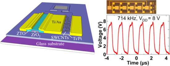
Figure 25. Schematic structure of an inkjet-printed SWCNT (p-channel) and ZTO (n-channel) based inverter, the optical micrograph of the 5-stage ring oscillator, and the output signal of the ROSC. Reprinted with permission from [123]. Copyright 2014 American Chemical Society.
Download figure:
Standard image High-resolution imageIn 2017, Chen et al developed inkjet printing of IGZO TFT arrays with small spacing using a metal nitrate based aqueous ink [125]. Aqueous ink is highly wettable on a SiO2 surface because of the hydrophilic characteristic of the SiO2 surface. To make the SiO2 surface hydrophobic, treatment with hexamethyldisilazane (HMDS) or octadecyltrichlorosilane (OTS) self-assembly was carried out. The minimum spacing (center-to-center distance) of the printed IGZO dot array decreased from over 80 μm to 45 μm and 35 μm with HMDS and OTS assembly treatment, respectively. To minimize the random drift of the ink drops, the ink viscosity was also adjusted by adding polyvinylpyrrolidone (PVP) to the ink solution. With the increase of ink viscosity, the random drift of the ink drops was suppressed and the smallest spacing was reduced to 50 μm for the printed oxide TFT arrays. The diameters and thicknesses of the printed indium oxide dots with different PVP concentrations and their optical image are shown in figure 26.

Figure 26. The diameters and thicknesses of indium oxide dots printed on HMDS-treated SiO2 substrates by using 0.02 M indium nitrate aqueous solutions with different concentrations of PVP, and photographs of inkjet printed indium oxide dot arrays on HMDS-treated SiO2 with a drop spacing of 50 μm by using 0.02 M indium nitrate aqueous solution with 0.1 mg ml−1 K30 PVP addition. Reproduced from [125] with permission of The Royal Society of Chemistry.
Download figure:
Standard image High-resolution imageThe inkjet-printed films generally show a non-uniform geometry due to the coffee-ring effect, which hinders their commercial application. The coffee ring effect is a phenomenon that is frequently observed in printed films. When the printed droplet reaches on the substrate, it spreads out and evaporates simultaneously. The evaporation rate on the edge region of drop is higher than that on the center region, inducing outward capillary fluid flow, carrying the solute to the edge of the droplet to replenish the evaporation loss at the edge, and resulting in a ring shape. Hu et al reported that the coffee-ring effect during the printing process can be suppressed to form uniform IGZO thin films by simply increasing the concentration of the ink, as illustrated in figure 27 [126]. The inkjet-printed IGZO TFT using laser spike annealing at a low temperature of 200 °C exhibited a mobility of 1.5 cm2 V−1 s−1, and an on/off current ratio larger than 106.

Figure 27. Optical microscopy images of inkjet-printed dots on SiO2/Si substrate obtained with precursor solution of (a), (b) 0.375 M and (c), (d) 1.5 M. [126] 2017 Springer Nature Copyright Center. With permission of Springer.
Download figure:
Standard image High-resolution imageIn 2018, the same group reported that the coffee ring effect can be suppressed or eliminated with the addition of an insulating polymer polystyrene (PS) to the ink [113]. The effect of the polymer molecular weight on the geometry, chemical composition, crystallization, and the resulting TFT properties were investigated. And they revealed that as the molecular weight of PS increasing to 200 000, the coffee-ring effect was completely eliminated due to the enhanced viscosity of the ink. The ink with enhanced viscosity has high resistance to the outward capillary flow, which prompt the depinning of the contact line, resulting in the disappearance of the coffee-ring. The optimized inkjet-printed In2O3 TFTs exhibited greatly improved mobility (13.7 cm2 V−1 s−1), with the addition of PS to the ink, due to the increase in the M–O concentration and decrease in contact resistance.
Subramanian et al demonstrated an fully-aqueous inkjet-printed In2O3 TFT with a mobility of 19 cm2 V−1 s−1, an on/off current ratio of 107 and a SS of 0.150 V/dec at a low processing temperature of 250 °C [60]. The InOx semiconductor layer was deposited by inkjet-printing from an aqueous solution of In(NO3)3 with a 40 μm drop spacing and a platen temperature of 30 °C. The intrinsic fluid properties of these water-based solutions enabled the printing of fine features with coffee-ring-free line profiles and smoother line edges than those formed from organic solvent-based inks. The aluminum-doped cadmium oxide acting as source/drain electrodes was also realized by the inkjet-printing technique from an ink composed of aqueous solutions of Al(NO3)3 and Cd(NO3)2.
With the help of surface-energy patterns, fully inkjet-printed InGaO TFTs, including inkjet-printed ITO electrodes and a ZrOx gate dielecric, were demonstrated by Lan et al [127]. The formation of the designed surface-energy patterns was realized by inkjet-printing pure solvent to etch the ultrathin Cytop hydrophobic layer. A ring, which acted as the separation bank, was formed at the edge of the surface-energy pattern owing to the coffee-ring effect. Each MO layer was then inkjet-printed onto the inside of the surface-energy patterns using the corresponding precursor inks. The schematic illustration of this process for each inkjet-printed layer using the surface-energy patterns is shown in figure 28. The surface-energy patterns were beneficial for the suppression of ink spreading and modification of the morphology of each inkjet-printed MO layer. The fully inkjet-printed InGaO TFTs exhibited good electrical performance, including a maximum mobility of 11.7 cm2 V−1 s−1, and relatively good uniformity and stress stability.

Figure 28. (I) Ultrathin Cytop layer deposited on substrate by spin coating. (II) Printing pure solvent to etch the Cytop layer. (III) Printing oxide precursor onto surface-energy pattern. (IV) Formation of oxide film after annealing. Reprinted with permission from [127]. Copyright 2017 American Chemical Society.
Download figure:
Standard image High-resolution imageIn 2018, Garlapati et al reported high performance inkjet-printed In2O3 TFTs using photonic curing (UV–visible light or UV-laser) without traditional high temperature thermal annealing process [128]. The fabricated In2O3 TFT exhibited a mobility of 25 cm2 V−1 s−1. Additionally, the threshold voltage of the TFTs can be simply adjusted through this photonic curing method to realize normally-on or normally-off states.
Later, the same group developed high-performance fully-printed MO TFTs with optimization of the interface between the electrode and channel [129]. The fully-printed TFT was composed of a-IGZO semiconductor, ITO electrodes, and solid polymer electrolyte gate dielectric. They revealed that Sn from ITO thin film substituted for Ga in the IGZO framework led to a diffused change of Fermi level at the interface, resulting in a perfect band alignment from the ITO electrode to the intermediate Sn-rich IGZO layer (or called a-ITZO). So the contacts between source/drain and channel became near-Ohmic contacts, which are beneficial for realizing high performance TFTs. Based on the proposed fully-printed unipolar a-IGZO TFTs, inverter logic circuits utilizing various kind of loading, such as resistor mode (R-mode), enhancement mode (E-mode), and depletion mode (D-mode) were fabricated and investigated. The inverters fabricated with sputtered ITO and printed a-IGZO TFTs showed the signal gain values of 2.6, 0.9 and 3.0 for R-mode (1 MΩ), E-mode and D-mode devices, respectively, at a VDD = 0.5 V.
Unlike the conventional contact printing techniques, aerosol jet printing, EHD printing and inkjet printing techniques are noncontact digital patterning techniques with resolution higher than that of the conventional contact printing techniques. However, the noncontact digital patterning techniques require adjustment of the ink viscosity, concentration and solvent system to the nozzle (to prevent clogging) and the substrate material. And spreading of the ink and wanted or unwanted merging of dispensed droplets needs to be controlled.
NIL is a high-resolution printing technique with patterning resolution less than 1 μm. Similar techniques such as hot embossing lithograph (HEL) and micro contact printing (μCP) have also developed for TFT fabrication. However, most of the reports on these techniques are for organic TFTs. So we will not discuss them in detailed in this review.
4. Gate dielectric engineering
The above sections have given a review on the MO semiconductors. In a typical TFT structure, the dielectric layer is placed between the gate electrode and the semiconductor. The properties of the gate dielectric layer and its interface with the semiconductor channel layer play a crucial role in the performance of the resulting TFTs devices. In another aspect, most of the gate dielectrics for MO TFTs are also metal oxides, so the process of gate dielectrics is similar to that of the semiconductors. Typically, four routes can be considered for the improvement of the gate dielectric: (1) increasing dielectric constant for high areal capacitance; (2) increasing bandgap and film density for low gate leakage current; (3) reducing defective states (e.g. dangling bonds, interstitial/substitutional defects); and (4) optimizing surface morphology and reducing charge-trapping interface states [39].
Solution-processed MO dielectrics have also been widely studied due to their large permittivity, excellent optical transparency, and good chemical/environmental stability. Numerous high-k MO dielectrics have been developed, including Al2O3, ZrO2, HfO2, Y2O3, La2O3, SrOx, Yb2O3, Nd2O3, MgO, Li2O, Sc2O3, Gd2O3 [59, 64, 66, 130–139], etc. In this section, we only focus on the development of the common solution-processed high k dielectrics (i.e. Al2O3, ZrO2, Yb2O3) in the past two years.
4.1. Al2O3-based
Binary solution-processed MO dielectrics are preferable because additives can be avoided in precursor solutions, resulting in a simple and low cost process. As discussed above, similar to MO semiconductor synthesis, different kinds of precursors and solvents were used for MO dielectric fabrication. As shown in figure 29, a nitrate-based precursor solution can be easily decomposed, with a sharp exothermic peak at 110 °C in the thermogravimetric-differential thermal analysis (TG-DTA) curve, owing to the volatile property of the nitrate ligands [81]. On the other hand, acetate- and chloride-based solutions were decomposed with step-like delayed mass reductions due to the non-volatile ligands involved. Unclear endothermic and exothermic chemical peaks at higher temperatures of ∼280 °C and ∼130 °C were observed for acetate- and chloride-based precursors, respectively. The nitrate based precursor solution can result in a higher quality Al2O3 thin film with higher M–O–M bond ratio and less number of M–OH bonding and other ligand-related impurities after the same post-annealing process, as compared to the other types of precursor solutions. The nitrate-based precursor has been the most widely adopted for sol–gel solution preparation due to its low impurity level, environmental stability, and low decomposition temperature.
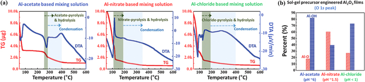
Figure 29. (a) TG-DTA curves of Al2O3 precursor solutions with different ligands: acetate, nitrate, and chloride. (b) Oxygen-related bond state ratios (Al–O and Al–OH) from sol–gel processed Al2O3 dielectric, which were annealed via sequential soft- (120 °C for 10 min) and hard-bake (300 °C for 30 min) processes. Reproduced from [81] with permission of The Royal Society of Chemistry.
Download figure:
Standard image High-resolution imageIn 2018, Peng et al developed a simple and effective method to improve the quality of the Al2O3 gate dielectric through adjusting the surface wettability of the substrates by an oxygen plasma-treatment process [140]. This O2 plasma treatment is a simple and effective way to improve the hydrophilicity of the substrate, especially for multilayer deposition because of the poor hydrophilicity of the each Al2O3 layer. The precursor solution was obtained through dissolving of aluminum nitrate nonahydrate in 2-methoxyethanol without any additives. The deposited Al2O3 films were dense, smooth, and uniform with coating layers larger than three. The optimized TFT with Al2O3 gate dielectric prepared by three-time spin coating showed a saturation mobility of 16.8 cm2 V−1 s−1, a threshold voltage of 2.5 V, and a subthreshold swing of 0.17 V/dec. Moreover, the a-IGZO TFTs devices also exhibited high negative gate bias stability.
Solution-processed Al2O3 and boron nitride (BN) composite films at a low process temperature were reported by Ha et al [141]. The Al2O3/BN mixed precursor solution was prepared by dissolving aluminum nitrite nonahydrate and BN powder in 2-methoxyethanol. A composite film of 41 nm thick Al2O3/BN was deposited by spin coating, followed by a microwave annealing for 15 min in an ambient atmosphere. During MWI, the temperature of the sample unavoidably increased to 150 °C. This work revealed that the incorporation of BN into the Al2O3 thin films can enhance the dielectric performance (e.g. lower leakage current, higher areal capacitance) without degrading the optical characteristics.
Ternary alloy aluminum yttrium oxide (Al2−xYxO3) films prepared by a low-cost spin-cast method was reported by Jeong et al [142]. The mixed precursor solution for the high-k Al2−xYxO3 dielectric was synthesized by dissolving aluminum nitrate hexa-hydrate and yttrium nitrate hexa-hydrate in 2-methoxyethanol with addition of nitric acid acting as an oxidant. The Al2O3 dielectric was selected to widen the bandgap of the Al2−xYxO3 dielectric films (lower the leakage current); and the Y2O3 dielectric was chosen as another component due to the higher dielectric constant (∼15). The Al2−xYxO3 thin films prepared with a post-annealing temperature of 400 °C exhibited smooth surface and excellent insulating characteristics due to structure stabilization from the cation alloying mixing effect. The IZO TFT with the ternary alloy Al0.45Y1.55O3 gate dielectric exhibited a mobility of as high as 52.9 cm2 V−1 s−1, a SS of 0.19 V/decade, an on/off current ratio of 4 × 10⁶, and no obvious hysteresis behavior. Moreover, they showed improved positive- or negative-bias-stress stability.
In addition, an environmentally friendly aqueous-based synthesis route for an AlOx dielectric was reported by Kim et al [143]. The AlOx precursor solutions were formed by dissolving aluminum nitrate hydrate in deionized water. The effect of the precursor solution temperature and humidity on the chemical, physical, and electrical properties of the AlOx dielectric was studied in detail. They found that more complexes related to the metal aquo complex were generated with a higher temperature of the precursor solution, which resulted in a higher density and better electrical performance of the synthesized thin film. In contrary, the AlOx thin film under humidity conditions of 30% or less during the spin coating process exhibited poor surface morphology, due to the spherulite structure generated, resulting in an increase of leakage current and a decrease of the breakdown voltage. With optimized conditions of the aqueous route-based AlOx gate dielectric (precursor solution temperature of 35 °C, humidity condition of 40%), solution-processed InOx TFTs were fabricated with a highest process temperature of 250 °C, and they exhibited high electrical performance, including field-effect mobility of 52 cm2 V−1 s−1 and on/off current ratio of 106. This aqueous route provides an inspiring and learning method for environmentally friendly, low-temperature, and high performance fully solution-processed MO TFTs.
Later, Cao et al also reported an aqueous route-based multi-component AlOx:Y dielectric [144]. With a small amount of yttrium dopant inside the AlOx framework. The resulting spin-coated AlOx:Y thin films exhibited much better performance, including smoother surface, better capacitance coupling, and smaller dielectric dispersion.
4.2. ZrO2
Zirconium dioxide (ZrO2) has attracted more and more attention in solution-processed high-k MO dielectrics owing to its high dielectric constant (∼25), wide bandgap (5.1−7.8 eV), high refractive index (2.17), and transparency [145]. Different from MO semiconductor thin films, solution-processed ZrO2 dielectrics generally require high annealing temperature to achieve dense structures for effectively blocking leakage current. Shan et al developed a water-inducement method to fabricate ZrOx thin films by a sequential process, including a UV-assisted photochemical treatment and a thermal annealing process at temperatures lower than 300 °C [64]. The water-inducement route allows the preparation of precursor solutes in water without additional additives and catalysts. The decomposition and the densification of water-induced (WI) oxide thin films can be achieved at lower annealing temperatures compared to those of organic-based precursors. It is observed that the leakage current density of ZrOx thin films decreased, and the capacitance increased with increasing annealing temperatures. Both n-type In2O3 and p-type NiOx channel layers were integrated with ZrOx dielectrics and their corresponding electrical performances were examined. The TFT with In2O3/ZrOx annealed at 250 °C exhibited an electron mobility of 10.78 cm2 V−1 s−1, and an on/off current ratio of around 106, while the p-type NiOx/ZrOx TFT exhibited a hole mobility of 4.8 cm2 V−1 s−1, and an on/off current ratio of around 105. Both n- and p-channel TFTs on ZrOx could be operated at voltages lower than 4 V.
Although ZrOx has attracted lots of attention in solution-processed MO TFTs, there are still some issues to be addressed for ZrOx application in displays. One of the challenges is the interface diffusion effect, the hydrogen diffuses seriously and acceptor-like defects occur. This effect will cause Vth negative shift and bias-stress instability for MO TFTs with ZrOx gate dielectrics, especially for top-gate MO TFTs. Recently, Lan et al reported a scandium-zirconium-oxide (Sc1Zr1Ox) dielectric for fully inkjet-printed top-gate MO TFTs [146]. They found that the incorporation of ZrOx and ScOx suppresses the hydrogen-ion migration and eliminates the acceptor-like traps. The printed InGaO TFTs based on Sc1Zr1Ox dielectric exhibited a highest mobility of 12.9 cm2 V−1 s−1 and excellent stability under both negative and positive bias stresses.
In 2018, Fong et al developed a low-temperature and high-quality ZrOx dielectric thin film utilizing a broadband UV annealing at process temperature of less than 120 °C [147]. The sol–gel solution was synthesized by dissolving zirconium acetylacetonate (Zr(C5H7O2)4) in N,N-dimethylformamide (C3H7NO) with the addition of ethanolamine (C2H7NO) and oleic acid (C18H34O2). A high quality ZrOx gate dielectric layer could be synthesized by one-step UV annealing without conventional thermal annealing step. The fabricated UV-annealed ZrOx dielectric thin film exhibited a high dielectric constant of 22.6 and a low leakage current of 10−9 A cm−2 at 1 MV cm−1.
Wang et al developed a simple and low-cost room-temperature UV-ozone-assisted solution-process method for ZrOx dielectrics from a precursor solution prepared by dissolving zirconium acetylacetonate (ZrAcAc) in an environmentally friendly solvent of ethanol [148]. A low leakage current of 6.0 × 10⁻⁸ A cm−2 at 3 MV cm−1 and high dielectric constant of 13 (at 100 Hz) were obtained for the optimized ZrOx dielectrics in nearly room-temperature process. It showed comparable electrical characteristics to those of the conventional thermal annealing process at 400 °C. It was revealed that numerous organic groups, which exist before any treatment, can be effectively eliminated after the UV-ozone treatment at room temperature. Finally, a fully room-temperature solution-processed InOx TFT with ZrOx gate dielectric was demonstrated. It exhibited an operating voltage of 3 V, a mobility of 1.65 cm2 V−1 s−1, and an on/off current ratio of about 104–105. This room temperature solution process route is a promising approach for flexible electronic applications.
Anthopoulos et al investigated the gate dielectric/semiconductor interface in In2O3 TFTs [149]. Three kinds of solution-processed high-k dielectrics, AlOx, HfOx, and ZrOx, were studied in detail. They revealed that the double spin-cast dielectrics exhibited consistently smoother layer surfaces, as compared to the single spin-cast ones. Improved electrical performance of the resulting In2O3 TFTs, especially significantly enhanced electron mobility, was observed.
4.3. Yb2O3
Shan et al reported an amorphous ytterbium oxide Yb2O3 gate dielectric prepared by spin coating with a precursor solution composed of ytterbium nitrate hydrate Yb(NO3)2·5H2O in N,N-dimethylformamide solvent [136]. A decomposition of residuals and densification process occurred with the increase of annealing temperature, which resulted in reduction of the leakage current. The fabricated Yb2O3 dielectric thin films exhibited an amorphous structure and smooth surface with high transparency (>85%) in the visible range. The optimized Yb2O3 dielectric exhibited a leakage current density of ∼10−8 A cm−2 at 1 V and a large areal capacitance of 352.8 nF cm−2 at 20 Hz. The resulting In2O3/Yb2O3 TFTs with an annealing temperature of 500 °C showed high electrical characteristics, such as field-effect mobility of 4.98 cm2 V−1 s−1, on/off current ratio of 106, turn-on voltage around 0 V, and SS of 70 mV/decade. Additionally, a unipolar inverter with a resistor load was further demonstrated and studied, which showed a highest output voltage that almost reached VDD and a lowest output voltage down to 0 V, implying full swing behavior of the proposed unipolar inverter.
For solution-processed high-k MO dielectrics, the mobile H+ ions should be considered seriously, because they would move to the dielectric/semiconductor interface and form electric double layer (EDL) which have extremely large capacitance. The EDL is unstable, and related to the air humility. Therefore, the mobile H+ ions should be removed or reduced for the practical applications especially in displays.
5. Applications
5.1. Active matrix display
The motivation for the research of MO TFTs is to meet the requirements for next-generation high-quality active-matrix displays, especially AMOLED or flexible displays.
In 2014, AU Optronics Corporation demonstrated a 4 inch flexible AMOLED display driven by solution-processed MO TFTs, as shown in figure 30 [150]. The spin-coating method was introduced to deposit the MO semiconductor film. The solution-based MO TFTs have saturation mobility of 4.02 cm2 V−1 s−1, sub-threshold swing of 0.39 V/decade, and threshold voltage of −0.69 V. The uniformity and electrical reliability for solution-based MO TFTs were also studied in this work.
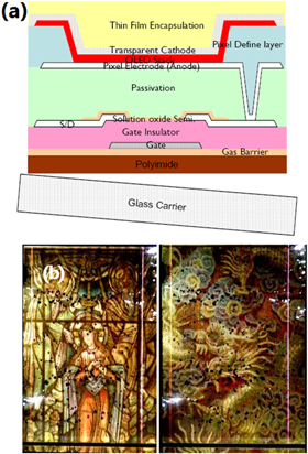
Figure 30. (a) Cross-sectional structure of the pixel with solution-processed MO TFT, OLED and thin-film encapsulation; (b) Photograph of the fabricated 4 inch AMQLED display with solution-process MO TFTs. [150] John Wiley & Sons. © 2014 Society for Information Display.
Download figure:
Standard image High-resolution imageEvonik Resource Efficiency GmbH developed a large-size solution-based coating method, slot-die coating technology, for MO TFTs backplane fabrication, which was integrated in a highly stable OLED display [2]. They scaled up the processes using mass-production-ready tools to fabricate the ESL type MO TFT backplanes. The fabricated a-IGZO TFTs exhibited high uniformity, good bias stress stability and high electrical characteristics. The proposed Linearcoater and a photograph of the 85 ppi AMOLED display are shown in figure 4.
Later, in 2018, Jang et al demonstrated a 4 inch active-matrix quantum-dot light-emitting diode (AMQLED) display with solution-processed MO TFTs which exhibited mobility over 5 cm2 V−1 s−1 over a 5 inch glass substrate [151]. The results indicate that the solution MO TFT based technology could be a promising technology for low cost display manufacturing.
Recently Lan et al demonstrated a quantum-dot light-emitting filed-effect transistors (LEFETs) (QD-LEFETs) using solution-processed MO semiconductors [152]. LEFETs have attained great attention, because it can act as a switching and an electroluminescence device. The QD-LEFETs combined high luminous-efficiency quantum dots (QDs) and solution-processed scandium-incorporated indium oxide (Sc:In2O3) semiconductor. The red QD-LEFET showed high electrical and optical performance with an electron mobility of 0.8 cm2 V−1 s−1, a maximum brightness of 13 400 cd m−2, and a maximum external quantum efficiency of 8.7%. The high performance of the QD-LEFET is attributed to the good energy band matching between Sc:In2O3 and QDs and the balanced hole and electron injection (less exciton nonradiative recombination). In addition, incorporation of Sc into In2O3 can suppress the oxygen vacancy and free carrier generation, and brings about excellent current and optical modulation (the on/off current ratio is 105 and the on/off brightness ratio is 106).
The first LCD display with solution-processed MO TFTs was also demonstrated by AU Optronics Corporation in 2013 [153]. The MO TFTs with spin-coated MO channel layers exhibited saturation mobility of 1.09 cm2 V−1 s−1, subthreshold swing of 0.84 V/decade, and the threshold voltage of −0.54 V. A 12.1 inch TFT-LCD driven by the solution-processed MO TFTs was demonstrated.
In 2018, a 5.5 inch LCD display driven by solution-processed MO TFTs with a back-channel etched structure fabricated by slot-die coating technology in the Gen 4.5 TFT-LCD production line was demonstrated [154]. High uniformity of the electrical performance for the solution-processed MO TFTs on Gen 4.5 glass was achieved. The prototype of the proposed 5.5' LCD is shown in figure 31.

Figure 31. Photograph of 5.5' AM-LCD driven by soluble MO TFTs with BCE structure. [154] John Wiley & Sons. © 2014 Society for Information Display.
Download figure:
Standard image High-resolution image5.2. Biosensor
TFT-based biosensing systems have been investigated comprehensively, because they have potential applications in portable or pocket-sized biosensors. MO TFTs have emerged as one of the best candidates for biosensors due to the advantages of their water, oxygen, temperature, and light sensibility. Ultrathin, uniform MO channel layer is required for the TFTs working on enhanced mode (normally off), because the carriers in the channel with a thickness within the Debye length (∼20 nm) is easier to be depleted.
A novel deoxyribonucleic acid (DNA) sensing system based on low-temperature solution-processed IZO TFTs has been developed by Kim et al [155]. The IZO precursor solution was prepared by dissolving indium nitrate hydrate and zinc nitrate hexahydrate in 2-methoxyethanol with the addition of nitric acid. A dry-wet method was applied to immobilize the target DNA oligomers onto the IZO back channel surface, after which a negative shift of the transfer curves was observed, accompanied by a significant increase in the on current and degradation of the on/off current ratio. A more negative shift of the transfer characteristics of IZO TFTs was observed upon guanine [poly (G)] immobilization with higher concentrations of 15 μM. Other types of DNA oligomers, such as cytosine [poly (C)] and adenine [poly (A)], showed similar trends after immobilization. The authors revealed that the sensing behavior was derived from the DNA oxidation instead of the conventional electrostatic force, promoted by the remaining reactive oxygen species on the IZO surface. Quantitative analysis on the relationship between the concentrations of DNA and the selective sensing in terms of the base sequence of DNA oligomers can be achieved with the IZO TFT sensors.
You et al proposed a solution-processed ZnO thin film with a thickness of 22 nm as an exposed sensing semiconductor channel to sense and identify different kinds of solution solvents, such as polar solvents (ethanol), non-polar solvents (toluene) and deionized (DI) water [156]. The proposed ZnO TFT sensor with a process temperature less than 300 °C exhibited an on/off current ratio of 107. The sensed solvents were dropped and adsorbed on the back-channel surface. The transfer characteristics of the ZnO TFT sensor were strongly dependent on the dielectric constant of the sensed solvents. The negative shift of the threshold voltage was caused by the extra electrons generated from the polar molecules accumulating on the ZnO channel. The proposed TFT sensing devices offer a method for low-cost, rapid and highly compatible solvent detection.
5.3. Artificial synapse
Ionic liquid (IL) gating has been extensively investigated due to its huge electrostatic capacitance in the form of ultrathin (∼1 nm) electrical double layers (EDL) at the IL/semiconductor interface [157]. In 2017, Mathews et al reported artificial synapses based on ionic-electronic hybrid oxide-based EDL transistors consisting of a semiconducting ZnO channel and an ionic liquid polymer dielectric (1-ethyl-3-methylimidazolium bis(trifluoromethylsylfonyl) imide (EMIM-TFSI)–poly(4-vinylphenol) (PVP)) on flexible polyimide substrates, as shown in figure 32 [158]. The proposed flexible transistor exhibited high electrical performance including a field-effect mobility of 9 cm2 V−1 s−1, and good mechanical performance. Systematic learning abilities or synaptic rules were investigated. It was revealed that the learning behaviors or synaptic rules were caused by a strong electrostatic coupling effect of ion migration-relaxation dynamics in the IL-polymer dielectric film. Paired pulse facilitation, high-pass filtering, excitatory and inhibitory postsynaptic currents, short-term to long-term memory transition, superlinear amplification, dynamic logic, and visual detection were successfully emulated and demonstrated.
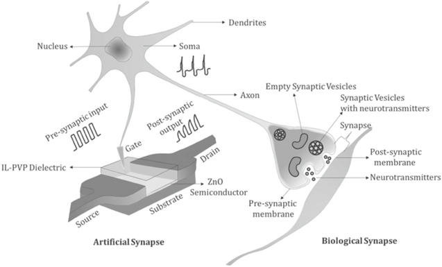
Figure 32. Schematic of a biological synapse and an artificial synapse based on ionic-electronic hybrid ZnO-based EDL transistor. [158] John Wiley & Sons. © 2017 WILEY‐VCH Verlag GmbH & Co. KGaA, Weinheim.
Download figure:
Standard image High-resolution image5.4. Nonvolatile memory
Nano-floating-gate non-volatile memory with gate dielectrics that contain nanoparticles has attracted much attention because it offers high scalability, low power, and high-speed operation for next-generation memory applications. In 2017, Lee et al reported non-volatile undoped/Hf-doped ZnO TFT memory realized by inserting gold nanoparticles (AuNPs) and AuNPs reduced graphene oxide (AuNPs-rGO) nanocomposite charge trapping media between undoped/Hf-doped ZnO and SiO2 [159]. A schematic diagram of the proposed devices is shown in figure 33. The ZnO TFT memories showed good programmable windows of up to 40 V during program/erase operations, which was attributed to the trapping and de-trapping of charge carriers by the AuNPs and the AuNPs-rGO nanocomposites. Both AuNP and AuNPsrGO nanocomposite-based undoped/Hf-doped ZnO TFT nonvolatile memory devices exhibited rewritable memory behavior with an on/off current ratio larger than 104 and stable retention times of 1000 s. In 2018, Fortunato et al reported that resistive switching memories (ReRAM) were developed and fabricated from a solution-based Al2O3 thin film using a simple combustion synthesis process [160]. The ReRAM devices showed unipolar resistive switching behavior with good endurance and retention time up to 105 s at 85 °C. A fully transparent ReRAM devices were realized by using ITO and IZO electrodes.
Figure 33. A schematic diagram of AuNPs and AuNPs-rGO nanocomposites inserted between semiconductor and gate dielectric layers. Reprinted from [159], Copyright 2017, with permission from Elsevier.
Download figure:
Standard image High-resolution image5.5. Photodetector
In 2016, Anthopoulos et al demonstrated high performance dye-sensitized phototransistors consisting of an ultrathin In2O3 thin film functionalized with a light absorbing organic dye D102 [161]. The post-annealing temperature was below 200 °C, enabling flexible application. The fabricated phototransistors showed a preferential color photoresponse centered in the wavelength of 500 nm, with a photoresponsivity of up to 2 × 10³ A W−1. The electrical gating of the photoactive channel enables the easy access into operating regimes, which is difficult to realize in conventional two-terminal photodetectors. The photosensitivity to green light of the proposed functionalized devices had a peak at VG = 10 V and a maximum value larger than 105. Meanwhile, the responsibility of the devices increased with increasing VG. At a gate voltage of −10 V, illumination with lower intensities exhibited a greater change in current per watt, as shown in figure 34. It was revealed that the response was cumulative over time until it reaches equilibrium, so the gains diminishing with increasing illumination intensity as there is less oxygen available to desorb, and hence a smaller photodoping effect.
Figure 34. (a) Photosensitivity and (b) responsivity of the D102-sensitized In2O3 transistors measured at different green light illumination intensities and as a function of VG at VD = 5 V. The inset in (b) shows the schematic of the D102-sensitized In2O3 phototransistor architecture employed. Reprinted with permission from [161]. Copyright 2016 American Chemical Society.
Download figure:
Standard image High-resolution imageIn the same year, Park et al developed an ultra-thin and large-area skin-compatible heterogeneous organic/metal-oxide photosensor array on a polyimide substrate, which had the functions of sensing and boosting signals with high detectivity and signal-to-noise ratio [162]. The skin-compatible heterogeneous photosensor array prototype was extremely light, and can be attached to the surface of polymeric wrap with an arbitrary shape or wrinkled skin, as shown in figure 35.
Figure 35. Ultra‐flexibility of 10 × 10 multiplexed heterogeneous photosensor system. (a), (b) Optical and (c) scanning electron micrographs of the ultra‐flexible heterogeneous photosensor circuit array under severe strains such as wrinkling with a plastic wrap, finger, skin, and a rolled-up state wrapping around the optical fiber (R ≈ 150 μm). (d) Comparison of the temporal photoresponse of the hybrid complementary circuit before and after severe mechanical strain (bent at R = 1 mm). The inset shows the photoresponse curves of the 20 different hybrid photosensor circuits randomly selected from the array. [162] John Wiley & Sons. © 2016 WILEY‐VCH Verlag GmbH & Co. KGaA, Weinheim.
Download figure:
Standard image High-resolution image
6. Outlook and perspectives
The recent advances in the development of solution-processed MO semiconductor devices are reviewed and summarized. Beginning with the engineering of the MO semiconductor materials, along with the optimization of precursors and the alternative annealing methods, solution-based MO TFT technology has gained great improvement in a short period of time, and will be at the core of many applications in the future, because the maskless and non-vacuum processes will be the mainstream to reduce the manufacturing cost.
One of the main motivations for developing solution-processed MO TFTs is to meet the requirements for next-generation FPDs. And some FPD demos with solution-processed MO TFTs have been demonstrated recently. Although only the MO channel layer were fabricated by solution process and the other layers were deposited by traditional vacuum-based processes, it is a big step for realizing the eventually fully-solution-processed (maskless- and non-vacuum-processed) TFT backplanes for FPDs. However, it still has a long way for commercialization of the solution-processed MO TFTs in the FPDs until the following key issues are properly addressed.
- (1)Large-area uniform and defect-free solution-processed deposition. A display usually has tens of million pixels, so controlling the defects in these tremendous number of pixels though the ambient-processed method is a big challenge.
- (2)High-resolution good-reproducibility patterning method comparable to the conventional photolithography technique. Compared to OLEDs, TFTs require patterning techniques with much higher resolution, because the channel size is usually less than 10 μm. Although some high-resolution printing methods such as aerosol jet printing and EHD printing have been developed recently, the process controllability of these novel printing methods is still not enough from an industry perspective. Therefore, the mechanical design of the printing systems for the stable and accurate delivery of ink droplets on large area substrates is impendency.
- (3)Precise layer-to-layer alignment. One of the obstacles for fully printing MO TFTs is the layer-to-layer-alignment inaccuracy, which generally leads to source/drain (S/D)-to-gate misplacement. As a result, large S/D-to-gate overlap should be design to make sure the channel is totally inside the gate region during printing, leading to reducing in resolution of the FPDs and increase in parasitic overlap capacitance. Moreover, in the conventional photolithography process, the substrate and the photomask will not move during exposure; in contrary, in the printing process, the nozzles move continuously, so the alignment is more difficult.
- (4)The long-term stability under bias, temperature, and light illumination, especially under negative bias illumination temperature stress (NBITS). As know the IGZO TFTs suffers from serious Vth shift under NBITS even fabricated with vacuum-processed method. As a result, a black matrix layer is required to block the light from illuminating into the channels. The solution-processed MO TFTs normally exhibits worse performances than the vacuum-processed ones. To the best of our knowledge, the stability of the solution-processed MO TFTs has not yet been examined under the criterions of industry mass-production application.
However, because of the great advance of the solution-processing techniques, these challenges do not affect people's great interest in the solution-processed MO-TFTs. The recent progress in fully-solution-processed OLEDs [163] raises the interest for fully-solution-processed AMOLED displays with both of fully-solution-processed OLEDs and TFTs. And the development of suitable printing techniques will contribute to the realization of a full R2R process for the low-cost, high-throughput, and large-area production of MO-TFT-related devices.
Taking into account the special properties of solution-processed MO semiconductors compared to silicon, they are not restricted to be used in AMLCDs or AMOLEDs display applications. Biosensors, artificial synapses, electronic price tags, and photodetectors, either on glass, flexible or paper substrates have already been presented.
Therefore, the maskless, non-vacuum solution-processed MO semiconductor based devices is a promising technology that not only may replace the conventional silicon technology in some applications but also opens new areas of applications.
Acknowledgments
We would like to thank the following organizations for funding us: the National Key R&D Program (Grant No. 2016YFB0401105), the National Natural Science Foundation of China (Grant Nos. 51673068, and 61204087), the Guangdong Natural Science Foundation (Grant No. 2017A030306007), the Guangdong Province Science and Technology Plan (Grant Nos. 2017A050503002 and 2016B090906002), and the Fundamental Research Funds for the Central Universities.