
Abstract
In this study, we investigate the effects of deposition parameters (i.e. gas flow rates, bias voltages, and nozzle-to-substrate separation) on the microstructure of <100 nm thick gold deposits made with a room-temperature, atmospheric-pressure, ion-drag microsputterer. Without resorting to the use of vacuum or substrate heating, optimization of the printing process yields dense, continuous deposits (96.5% coverage) with low electrical resistivity (45 μΩ cm). Using statistical analysis, we developed a simple model that provides insight into the dynamics of such a printing method; based on this model, we identify electrostatic effects as the most important factor that influences the deposition process.
Export citation and abstract BibTeX RIS

Original content from this work may be used under the terms of the Creative Commons Attribution 3.0 licence. Any further distribution of this work must maintain attribution to the author(s) and the title of the work, journal citation and DOI.
1. Introduction
The last two decades have seen a flurry of work on novel methods for additive manufacturing (AM) –processes that create parts by simply depositing material where it is needed, instead of removing material from stock [1]. Besides waste reduction, AM poses other key advantages over traditional fabrication such as rapid prototyping, print-to-print customization, and cost and time savings when making small batches and complex parts. An exciting research track in AM is functional multi-material printing, that is, the development of printing technologies to manufacture objects that are functionally complex by virtue of being made of a plurality of finely layered materials that are optimized to accomplish a certain task [2]. In particular, AM of metal interconnects has been actively pursued with varying degrees of success for electronics and other microsystems [3]. However, most of the reported methods suffer from low resolution, poor electrical conductivity, the need for post-processing to achieve adequate electrical properties, incompatibility with low-temperature substrates, e.g. flexible electronics, or some combination thereof.
Sputtering is the manufacturing method used in state-of-the-art electronics to produce thin, conformal coatings of nearly any material. In sputtering, a plasma is formed between two electrodes; the positively-charged ions are accelerated by a voltage gradient towards the cathode electrode, also called the target; these ions strike the target surface with sufficient force to dislodge atoms, which then travel, either ballistically or with collisions, to a nearby substrate, adhere to it, and form a conformal coating [4]. The first particles to land simply stick to the substrate at the point of impact. However, as the substrate surface fills in, the deposited particles prevent incoming particles from reaching the substrate; instead, the impinging particles encounter already-deposited particles and stick to them, forming grains that grow vertically and horizontally, leaving narrow chasms between converging grains. No newly-sputtered particle can navigate these narrow chasms: a shadowing effect causes the arriving particle, often approaching the substrate at an angle, to join the top of an existing grain rather than to navigate the chasm between the grains. As a result, the chasms remain, even as the deposit grows, creating a porous microstructure that increases the material's electrical resistivity.
Thornton's zone model [5], developed in the 1980s and still accepted in large part, adopts the previously described basic mechanism as the driver of the film microstructure, and identifies two crucial conditions that can affect the grain formation. First, background pressure controls the number of collisions that a sputtered atom will undergo between its ejection from the target and its impact onto the substrate: the more collisions the sputtered atom experiences, the more likely the atom will strike an existing grain instead of traveling in its original direction of motion, normal to the substrate surface, through a chasm towards the substrate. Second, the substrate temperature controls the surface mobility of the impinging atom. At high temperatures (>30% of the melting temperature of the film), thermal effects allow arriving atoms to move into energetically favourable positions within the chasms, increasing the film density. Consequently, industrial sputtering processes, such as those used in complementary metal-oxide semiconductor (CMOS) fabrication, work at high vacuum and at high substrate temperatures. However, strict temperature control is necessary to achieve the desired pore-free, electrically conductive microstructure while not damaging previously fabricated structures or the substrate. For agile manufacturing, these constraints on vacuum level, substrate, and process temperature are not desirable, and Thornton's zone model does not suggest an acceptable set of parameters.
We thus turn to a slightly different zone structure model [6]. Mahieu et al building on work by Messier et al [7], restates Thornton's first parameter, pressure, as bombardment velocity. In this model, if a sputtered atom has sufficient kinetic energy while impacting the substrate, the atom's mobility will allow it to move into a more energetically favourable position between two grains; with enough energy, it can even modify crystalline grain boundaries, allowing grains to merge [8, 9]. The kinetic energy does not need to be carried by the atoms as they arrive at the substrate; ion-beam-assisted deposition techniques enable the modification of thin-film microstructure and electrical and mechanical properties, during and after film deposition, by passing an ion beam over the film, eliminating grain boundaries by applying energy to move sputtered material into more energetically favourable positions [10]. Nonetheless, it is preferable to provide additional energy to the atoms prior to substrate impaction, before they are fully bound to the deposited film; additionally, if the sputtered atoms carry the non-thermal kinetic energy, they will all arrive to the substrate at approximately the same angle. Sputtered atoms with insufficient energy will form tall, closely packed, and narrow columnar grains, with crystallographic orientation determined by the angle of arrival. Because the angle of arrival is parallel to the column wall, atoms are able to enter inter-granular chasms, shrinking their width over time. This process has been harnessed to create columnar microstructures, at both right and oblique angles, to create films with tuned light transmissivity [11].
Electrostatic attraction can be another effective method for ensuring that the arriving atoms have enough kinetic energy for grain reorganisation given that sputtering plasmas contain a fraction of ionized gas. Therefore, a negatively biased substrate can draw these ions towards the substrate at velocities needed for grain reorganization [12, 13]; similarly, plasma lenses can also help direct the ions [14]. Electrostatic attraction has been recently used in high-power impulse magnetron sputtering (HiPIMS), which uses high currents applied in short pulses (impulses) at low duty cycle to ionize a large fraction of sputtered material. By applying a negative bias voltage to the substrate, the ionized material impacts the substrate with large velocity, forming a smooth and continuous layer [15, 16]. However, too much electrostatic attraction can lead to re-sputtering, in which the sputtered atoms do not adhere, but rather bounce off the substrate. In extreme cases, they will dislodge substrate material, resulting in ion etching [17, 18]. All of these electrostatic-based methods are predicated on the ionization of a large fraction of the sputtered material—a difficult procedure that requires specially shaped plasmas, often diminishing the deposition yield of the process [13].
Paschen's scaling law states that the behaviour of a plasma is fundamentally governed by the product of the inter-electrode distance and the gas pressure [19]. Microplasmas take advantage of this to operate at atmospheric pressure by restricting the inter-electrode distance to millimetre-scale or smaller. Researchers have reported using microplasmas to create metal imprints at atmospheric pressure [20–22]. These reactors use the sputtering microplasma to anneal their deposits, resulting in imprints with fairly high electrical conductivities; nonetheless, in order to use microplasma sputtering in agile manufacturing of electronics, whether to print circuits ab initio, rework damaged circuits, or add interconnects to existing devices, generating deposits with low electrical resistance at a low deposition temperature is essential.
Electrostatic attraction has been used to modify the deposition characteristics of atmospheric pressure plasmas. At high pressures atoms collide frequently and lose part of their momentum, limiting the velocity that can be imparted by external fields; nevertheless, electric fields do have an effect on the characteristics of the imprints. While this effect has been studied in copper oxide films [23, 24], non-reactive depositions, which are relevant to our application, have not yet been studied. Furthermore, the reported work primarily explored the chemical composition, rather than the physical microstructure, of the deposits. We recently reported a novel ion-drag-focused, atmospheric pressure microplasma sputterer designed to directly print high-resolution, conductive features without the need for post-processing, e.g. annealing [25]. We use a combination of a directed gas flow and electrostatic attraction to ensure that the sputtered material reaches the substrate with a high normal velocity, while minimizing substrate heating. In this paper, using an improved microplasma reactor, we explore the effects of deposition parameters on the microstructure and electrical resistivity of sub-100 nm thick gold films, looking to optimise the printing process and gain insights into the parameters that govern the creation of void-free, highly conductive films.
2. Methods
The atmospheric microplasma printhead (figure 1) has a target electrode comprised of a continuously-fed gold wire (Sigma Aldrich, 50 μm diameter, purity >99.99%) surrounded by a glass pipette with 750 μm inner diameter (the inner capillary in figure 1), which in turn is encircled by four laser-cut stainless steel electrodes evenly spaced around a 5-mm inner diameter glass tube (the outer capillary in figure 1) and 6 mm away from the target wire. Two anode electrodes on opposite sides of the target wire are positively charged; the other two focus electrodes, also on opposite sides but offset by 90° with respect to the anode electrodes, are negatively charged to concentrate the positively charged plasma and, through ion drag, the sputtered material into a narrow line. The target is grounded, the focus bias voltage is provided by a 6516A HP DC power supply, and the anode bias voltage is provided by a Keithley 2657A power supply, modulated to maintain a constant 1 mA current. The electrodes are attached to a 3D-printed block with grooves for each electrode, enabling robust electrode alignment during assembly and ensuring repeatable printing. The laser-cut electrodes in this second-generation printhead are improvements to the manually-shaped tungsten electrodes previously reported in [25]; although tungsten is more resistant to sputtering than stainless steel is, energy-dispersive x-ray spectroscopy (EDX) measurements of the imprints confirmed that the electrodes are not sputtered during the process, thereby relaxing the constraints on their constitutive material. A laser-cut Kapton shadow mask can be affixed to the printhead to further narrow the imprints or to directly transfer a pattern to the substrate without moving the stage; however, the majority of the samples used in this study were created without using a shadow mask.
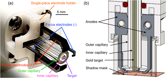
Figure 1. Close-up photograph (a) and 3D schematic (b) of the printhead. The (nearly invisible) gold wire is surrounded by two gas flows separated by a small glass capillary. A set of four electrodes surrounds the target wire. The sputtered metal is ejected from the target wire; in the photograph's orientation, it would fly out of the page, while in the schematic's orientation, it flows downward. The schematic shows the printhead fitted with an optional shadow mask. In this study, the majority of the imprints were created without using a shadow mask.
Download figure:
Standard image High-resolution imageIn the experiments reported in this study, the printhead assembly is positioned so that the anode electrodes, focus electrodes, and target wire are in plane (see bottom of figure 1(b)), between 255 μm and 760 μm above the substrate—a 0.7 mm thick piece of silicon wafer coated with a 500 nm thick film of SiO2. The separation distance is controlled with a 25 μm resolution calliper. The feed of the target wire is controlled by a stepper motor attached to a capstan-and-roller mechanism; the vertical position of the free end of the wire can be controlled to within 50 μm, enabling continuous feed of the target to the microplasma reactor. Visual inspection ensures that the wire tip, and consequently the area that is sputtered, is kept vertically aligned with the electrodes. Argon flows through the inner and outer capillaries are independently controlled by analogue UFC-1000 mass flow controllers. The outer flow rate (i.e. gas flow rate through the outer capillary) controls the gas composition of the atmosphere surrounding the electrodes; this flow rate is chosen to ensure an anode-to-target voltage drop between 700 and 1100 V (these bias voltage values were determined experimentally to attain reasonable deposition rates, without overheating the central wire or the substrate). A gas flow rate of 0–139 sccm yields the appropriate argon-air blend to maintain the desired bias voltage.
To screen for significant parameters, a statistically-designed experiment (DOE) was performed on a total of 33 printed samples (table 1). In the DOE, five process parameters were varied, i.e. (i) separation between the printhead and the substrate, (ii) focus electrode bias voltage, (iii) bias voltage or its absence on the aluminium foil beneath the substrate (figure 2), (iv) gas flow rate through the inner capillary (inner flow rate), and (v) outer flow rate. The DOE fully explored three different distances and three different focus electrode bias voltages (i.e. a 32 full factorial design); the state of the aluminium foil and inner flow rate were determined on the basis of those parameters. This approach resulted in 25 samples (multiple samples were collected for several of the sets of parameters); the remaining eight samples were chosen from regions outside the core parameter space and were meant to exaggerate the effects of parameters. The outer flow rate and the anode-to-target bias voltage were recorded for each deposition and analysed. There were three kinds of deposits printed in the experiment: (i) material deposited by keeping the printhead stationary for 15 min—spots; (ii) material deposited by passing the printhead 30 times over a region at a rastering speed of 40 μm s−1—unmasked lines; and (iii) material deposited through a shadow mask (figure 1(b))—masked lines. Given that in previous experiments we found the microstructure of the deposit to be independent of masking or rastering, we did not track these as variables in our DOE. The lack of effect is reasonable; given that the rastering speed is at least six orders of magnitude smaller than the thermal velocity of the sputtered material, it can easily be neglected. However, the deposition conditions were recorded.
Table 1. Printing parameters and estimated film coverage for the 33 samples analysed in this study. Foil charged/floating status, printhead-to-substrate gap, focus and foil voltage (when biased), and inner gas flow rate were determined in accordance with a DOE. The outer gas flow rate was chosen for each deposition to ensure that the anode bias voltage remains within an acceptable range. The anode bias voltage was a dependent parameter adjusted to maintain 1 mA current in the plasma. The type of deposit was determined from previous tests not to make a difference, and was thus not part of the DOE. Data are first grouped based on whether the substrate was charged, then sorted in ascending order by the parameters identified as most relevant in the DOE analysis (i.e. focus bias voltage for the charged substrate case, printhead-to-substrate gap size for the uncharged substrate case).
| Charged substrate | |||||||
|---|---|---|---|---|---|---|---|
| Sample # | Type of deposit | Printhead-to-substrate gap (μm) | Focus (and foil) bias voltage (V) | Inner flow rate (sccm) | Outer flow rate (sccm) | Anode bias voltage (V) | Film coverage (%) |
| 25 | Masked line | 510 | 0 | 15 | 56 | 850 | 63 |
| 26 | Masked line | 510 | 0 | 15 | 83 | 970 | 78.1 |
| 27 | Spot | 255 | 0 | 15 | 61 | 910 | 56 |
| 28 | Spot | 635 | 0 | 15 | 56 | 880 | 74.3 |
| 4 | Spot | 255 | 100 | 15 | 28 | 796 | 85.6 |
| 5 | Spot | 635 | 100 | 15 | 83 | 800 | 88.9 |
| 6 | Spot | 510 | 100 | 25 | 42 | 830 | 79.4 |
| 17 | Spot | 510 | 100 | 15 | 111 | 900 | 74.9 |
| 18 | Unmasked line | 510 | 100 | 25 | 139 | 920 | 69.9 |
| 2 | Spot | 760 | 300 | 15 | 139 | 850 | 87.7 |
| 7 | Spot | 510 | 300 | 15 | 42 | 810 | 95.4 |
| 9 | Masked line | 380 | 300 | 5 | 56 | 840 | 85.1 |
| 15 | Spot | 380 | 300 | 5 | 111 | 910 | 52.1 |
| 16 | Spot | 510 | 300 | 25 | 111 | 910 | 93.3 |
| 19 | Unmasked line | 510 | 300 | 15 | 83 | 980 | 82.8 |
| 29 | Spot | 760 | 300 | 15 | 83 | 820 | 44 |
| 30 | Spot | 760 | 300 | 15 | 83 | 770 | 34 |
| 31 | Spot | 760 | 300 | 15 | 83 | 780 | 90 |
| 32 | Spot | 760 | 400 | 15 | 83 | 820 | 91.9 |
| 33 | Spot | 760 | 500 | 15 | 83 | 965 | 96.5 |
| Floating substrate | |||||||
| 8 | Spot | 380 | 300 | 5 | 42 | 830 | 77 |
| 10 | Masked line | 380 | 300 | 25 | 56 | 850 | 81.6 |
| 11 | Masked line | 380 | 100 | 15 | 70 | 860 | 79.8 |
| 13 | Spot | 380 | 100 | 5 | 111 | 765 | 49.3 |
| 14 | Spot | 380 | 300 | 15 | 111 | 770 | 87.4 |
| 20 | Unmasked line | 380 | 0 | 5 | 83 | 800 | 90.4 |
| 21 | Unmasked line | 380 | 300 | 5 | 83 | 790 | 93.5 |
| 12 | Spot | 510 | 100 | 5 | 70 | 790 | 75.4 |
| 22 | Unmasked line | 510 | 0 | 15 | 111 | 910 | 65.9 |
| 23 | Unmasked line | 510 | 100 | 15 | 139 | 970 | 89.3 |
| 24 | Masked line | 510 | 100 | 25 | 28 | 940 | 45.3 |
| 1 | Spot | 635 | 100 | 25 | 139 | 970 | 51.1 |
| 3 | Spot | 635 | 300 | 25 | 139 | 690 | 62 |
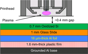
Figure 2. Schematic cross-section of the structure that holds the substrates. The aluminium base is grounded; a plastic film electrically isolates the base from an aluminium foil, which can either be negatively biased or left floating. A glass slide sits on top of the foil. The printhead is right on top of the substrate; the printhead can move vertically with the use of a manual stage, and can be moved parallel to the substrate using PC-controlled stages.
Download figure:
Standard image High-resolution imageThe printed samples were imaged using a Zeiss 1525 scanning electron microscope (SEM) with a beam voltage equal to 10 kV and a resolution of approximately 4 nm. The images were analysed numerically using Wolfram Mathematica; an estimate of film coverage (i.e., proportion of the film that is solid, void-free) was obtained by modelling the frequency of the grey shading of the pixels as the sum of two Gaussian functions: one for the lighter pixels –signifying a gold deposit, and a second for the darker pixels –signifying bare substrate.
3. Results and discussion
Figure 3 shows a representative SEM of an imprint and the functional decomposition of the colour of its pixels as two Gaussian curves. The two curves overlap (figure 3(b)); however, by modelling the grey shading distribution of each image as a sum of Gaussian curves, an accurate coverage estimate can be obtained without directly resolving the status of intermediately-coloured pixels.
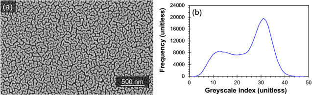
Figure 3. A micrograph of sample 27 (a), and frequency distribution of its pixels' grey shading (b); the index is the shade of grey in the 8-bit (256 colours) greyscale output of the SEM; the larger the index, the lighter the shade. In Figure (b), two overlapping bell-shaped curves are visible; the curve on the left represents the darker pixels, i.e. where bare substrate is visible, while the curve on the right represents the lighter pixels, i.e. where gold covers the substrate.
Download figure:
Standard image High-resolution imageAcross all samples, the film coverage ranged from 34% to 96.5% (table 1). While these estimates do not consider cracks smaller than the image resolution, we surmise that process improvements that minimize resolvable cracks will, at least to first order, also minimize the incidence of these small cracks in the film coverage. The micrographs shown in figure 4 reveal two distinct morphologies, i.e. isolated droplet patterns (associated with low film coverage) and meandering patterns (associated with high film coverage). As film coverage increases, the meandering regions of gold become larger and the gaps between them become smaller. The samples with droplet patterns were removed for later analysis, and the remaining samples were split into two groups –with and without bias voltage applied to the aluminium foil under the substrate (see figure 5). For this analysis a simple linear model is assumed (as is appropriate for small variations in parameters), where the film coverage of the jth sample, Cj, can be predicted as

where ai is the ith coefficient of the model and xi,j is the ith deposition parameter of the jth sample. Note the presence of ao, the constant term, which represents what the film coverage would be if the other parameters were all equal to zero. Given that such a condition is outside the useful range of our model, the term has no simple physical significance. The best fit of equation (1) was found for each case by adjusting the values of the ai coefficients, each of which represents the dependence of the coverage on the associated parameter. In equation (1), the coefficients can be positive or negative, evidencing whether a positive change in the corresponding parameter makes the imprint coverage increase (positive coefficient) or decrease (negative coefficient). After finding the best fit using all of the deposition parameters of the model, the terms that are not statistically significant are removed. A graphical representation of the effects of various parameters is given in figure 5. The statistical significance in the caption of figure 5 is given by the t statistic, a quantity that is derived from Student's t test that represents how significant the estimated mean effect is, in comparison with the noise associated with that effect [26]. The associated p-value represents the chance that a random sampling, i.e. one with no dependence on a given parameter, would display a (spurious) effect at least this strong. Given that the proper interpretation of this statistic in cases where multiple hypotheses, particularly related hypotheses, are tested is a matter of much debate [27], in all cases we provide the p-value of the statistic without any adjustment.
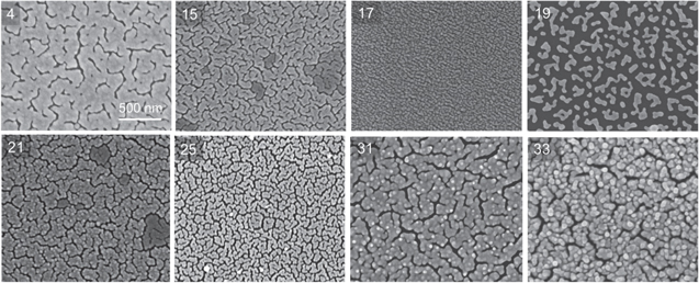
Figure 4. Micrographs of selected printed samples. Imprints with meandering patterns (samples 4, 15, 21, 25, 31, and 33) and isolated droplet patterns (samples 17 and 19) can be identified. Lighter regions represent gold deposits; darker regions represent bare silicon dioxide. In samples 15 and 21, mid-dark regions are electrically isolated from the lighter regions, causing sample charging and a difference in greyscale intensity.
Download figure:
Standard image High-resolution image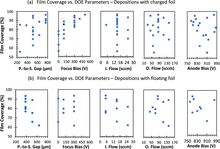
Figure 5. Series of scatter plots relating deposition parameters with film coverage for depositions done with a charged foil (a) and with a floating foil (b). It is apparent from the data that there is no discernable pattern in the majority of cases; the exceptions are the focus bias voltage (which includes the foil voltage) in the case of the charged foil (t-statistic 4.72), and the printhead-to-substrate separation and, to a lesser extent, the outer flow rate, in the case of the uncharged foil (t-statistics of 2.59 and 1.86, respectively). The unadjusted p-values, or the chance that a random fluctuation would result in such a t-statistic or one higher, for those parameters are 6.31 × 10⁻⁵, 6.1 × 10⁻², and 1.36 × 10⁻¹, respectively; the proper interpretation of these values is briefly discussed in the text.
Download figure:
Standard image High-resolution imageWith the reduced set of deposition parameters, we constructed a simplified, yet effective model for each group, i.e. meandering films created with and without bias voltage applied to the foil under the substrate. The analysis concludes that the inner gas flow rate and the anode bias voltage had no effect on either of the trends. In addition, the statistical analysis conducted shows two clear trends:
- (i)If the foil under the substrate has a negative bias voltage applied, the film coverage increases if the magnitude of the foil voltage augments (figure 5). To understand this trend, we return to a close-up micrograph of one of our deposits—sample 33 (figure 6). Small nanoparticles, approximately 25 nm in diameter, are clearly visible. It appears (as has also been observed by Lazea-Stoyanova et al [28]) that sputtered metal agglomerates as it travels between the printhead and the substrate. A 25 nm diameter nanoparticle will have approximately 260 000 gold atoms (assuming a packing density of approximately 0.6 [29]); some small fraction of those atoms will be ionized. Each nanoparticle is drawn to the negatively biased foil, allowing it to strike the substrate with significant velocity, approximately normal to the surface. The size of the gap between the substrate and the printhead does not influence this effect significantly; once the nanoparticle forms and is ionized, it is not considerably affected by collisions with much lighter particles. This effect can be exploited to deposit individual nanoparticles on a substrate; such results have been shown by other researchers [28], albeit without the ionization of these nanoparticles. In contrast to other methods in which electric fields are used to improve material quality [12–16], the sputtered material in our case is not heavily ionized. Instead, a small fraction of the sputtered material is ionized; at atmospheric pressure, nanoparticles form and allow even a low degree of ionization, combined with electric fields, to improve material quality.
- (ii)In contrast, when the foil is not biased, there is no strong gradient guiding the nanoparticle towards the substrate; in fact, nanoparticles of this size are not evident in any of the samples produced with the use of the foil floating, even under high magnification. If the foil under the substrate is left floating, the film coverage increases when the printhead is closer to the substrate and when the outer flow rate is higher (figure 5). A higher outer flow rate causes a larger volume fraction of argon to surround the plasma. Argon is more likely to be ionized than nitrogen, in large part due to its monoatomic structure (no energy is spent breaking chemical bonds). Additionally, argon is heavier than atomic nitrogen (which would be the main form of nitrogen to be ionized—molecular nitrogen will break apart at the energies necessary for ionization to happen), and is thus more effective at imparting momentum to the sputtered material through ion drag. Therefore, the higher the argon content, the stronger the influence of the electrical field in the sputtered gold's motion, and the faster the sputtered material will move towards the substrate. However, the plasma rapidly recombines as it drifts away from the target wire and surrounding area of high electric field and ion density, known as the positive column. As the voltage gradient decreases, ions are less likely to gain the necessary momentum to ionize as many particles as they do in the positive column. Thus, any momentum gained by the sputtered material is likely to be gained near the target wire; the farther the sputtered material moves from the positive column, the less effect ion drag will have on its dynamics. Consequently, as the gap between the target wire and the substrate increases, the particles are more likely to return to thermal equilibrium, and the microstructure suffers. In contrast to the case previously discussed (biased foil), nanoparticles do not form and thus, the gold can be slowed once it leaves the highly ionized region. Nevertheless, this case is also innovative; rather than ionize a large fraction of the sputtered material, we merely ionize a small fraction of the working gas and sputtered material and allow ion drag, at atmospheric pressure, to transfer the electric force to the neutral sputtered material.
During the creation of the imprints, the electrostatic forces are far larger than those imparted by the gas flow; this can be easily verified with a rough estimate of the power in the ion flow and in the flow of neutral molecules:
- (i)As a conservative model, we assume that the plasma's ions are confined within a 50 μm thick hemispherical region surrounding the target wire and positive column. Each ion is accelerated from rest by the electric field until it collides with a neutral atom, at which point it transfers all of its momentum to the neutral atom and returns to rest. With a mean free path of 50 nm for air at atmospheric pressure, and an electric field towards the substrate of 0.8–1 MV m−1 (estimated via COMSOL simulations), each ion will gain 0.04 eV of energy between collisions, which occur every 125 ps per ion. If we assume that the ions make up 0.1% of the plasma, for a total of 1010 ions, the ions direct about 0.64 W towards the substrate. While these calculations are done for a negatively biased substrate, similar calculations can be done for floating substrates; the energy is of the same order of magnitude.
- (ii)In contrast, the inner flow rate in the printhead is on the order of 25 sccm and flows through a 750 μm diameter tube, resulting in a muzzle velocity (i.e. when the gas exits the tube) of 0.95 m s−1—neglecting compressibility effects. Therefore, the power in the flow is about 3.35 mW, which is orders of magnitude smaller than the estimate of the power in the ions due to electrostatic effects. While previous simulations of our ion drag microsputterer have shown the importance of the inner gas flow [25], they merely reflect the fraction of the sputtered material that reaches the lower end of the positive column, at which point electrostatic effects carry the sputtered material towards the substrate.
We also applied our simplified model to the six samples that presented isolated droplets as imprint morphology instead of meanders (i.e. samples 13, 15, 24, 27, 29, and 30). Based on our model, two of the samples were predicted to have low film coverage (<60%), and four of the samples were predicted to have high coverage (>85%). The two samples with expectedly low film coverage require no explanation as they line up well with our model predictions (figure 7). For the four remaining samples with greatly overestimated film coverage predictions, we speculate that the sputtered material in these samples struck the substrate with too much force and did not adhere. This is supported by similar observations in the literature, in which particles that are too energetic do not adhere to the substrate [17, 18].
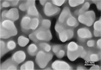
Figure 6. A high-magnification micrograph of sample 33 (the sample with the most film coverage attained in the DOE). Individual nanoparticles make up a large portion of the deposit. There is evidence of coalescence of the nanoparticles, although many chasms are still evident, due to the limited depth of focus of the SEM at high magnification. This characteristic nanoparticle microstructure only appears for deposits with negatively biased foil beneath the substrate.
Download figure:
Standard image High-resolution image
Figure 7. Comparison of actual film coverage and film coverage predicted by our simplified piece-wise model. The round dots, symbolizing meandering deposits, are closely correlated with the predicted coverage. The triangular dots, symbolizing deposits that presented an isolated droplets structure (13, 15, 24, 27, 29, and 30), fall into two categories; two of the samples fit the model, while the other four have predicted film coverage greatly surpassing the actual coverage; independently, the isolated droplets structure data set does not fit our model (e.g. the corresponding least squares linear fitting has negative slope and R2 ∼ 0). A least squares linear fitting shows good agreement between our model and the 27 meandering samples (a), and with the combined data set of 27 meandering samples and the two droplet samples that fit the model (b).
Download figure:
Standard image High-resolution imageOf the four isolated droplet samples not satisfactorily described by the model, three were produced while the foil was biased at a large negative voltage (−300 V), and one was produced with a floating foil and a small 380 μm substrate-to-printhead gap. Based on our simplified model, these conditions should produce imprints with high film coverage due to the large velocity of the sputtered material; in reality, these conditions produced sputtered particles with such a high velocity that did not stick to the substrate, resulting in poor film coverage. Our simplified model does not explain why some combinations of parameters produced high-velocity particles that stuck to the substrate creating dense imprints, while other slightly different combinations produced high-velocity particles that were too energetic to stick to the substrate. For example, samples 29, 30, and 31 were produced with identical conditions, with the exception of a small difference in the anode bias voltage. However, samples 29 and 30 present an imprint structure of isolated droplets, while 31 presents dense meanders. Perhaps our study did not identify all of the key factors to consistently produce high-quality microsputtered depositions; nonetheless, the model shows the general mechanisms involved in the creation of the deposit.
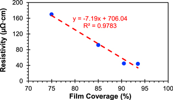
We also examined the dependence of the electrical conductivity of the deposits on the imprint coverage, focusing on measuring printed lines made of films with high coverage. However, due to the ultrathin nature of the deposits we were able to print, we found it difficult to measure the electrical resistivity without the probes damaging the samples (gold has inadequate adhesion to silicon dioxide). However, we were successful at characterizing the electrical resistivity of four samples with ∼75%–95% film coverage (figure 8). The data show the expected negative correlation between electrical resistivity and substrate coverage, confirming the expectation that by improving film coverage, electrical conductivity is also improved. We measured imprints with electrical resistivity as low as 45 μΩ cm—approximately 18 times the resistivity of bulk gold. It is possible that imprints with near-100% coverage are more conductive; perhaps the deposition of thicker films would yield even more conductive imprints. The smallest electrical resistivity measured in our study is slightly larger than reported values of other printing technologies that do not use annealing [30], e.g. laser-induced forward transfer (LIFT, with resistivity of 12 times bulk metal [31]), and is also larger than reported values from annealed microsputtered deposits [20]. However, our technology compares favourably with other direct-write methods for fine-featured metals, e.g. unannealed nanoparticle inks (with a 50-fold increase in electrical resistivity compared to bulk metal [32]), demonstrating its viability as a technology for agile manufacturing of interconnects for flexible electronics and other microsystems incompatible with high-temperature processing.
Figure 8. Electrical resistivity versus film coverage of microsputtered gold lines. These imprints are associated with a meandering film structure. The data support the trend that the more complete the coverage of an imprint, the lower its resistivity. A least-squares linear fitting fits the data well.
Download figure:
Standard image High-resolution image
4. Conclusion and future work
Using a DOE, we experimentally investigated the effects of deposition parameters on the microstructure of room-temperature, atmospheric pressure, ion-drag-focused sputter deposition. In doing so, we have shown that is possible to produce continuous (96.5% coverage), highly electrically conductive deposits (45 μΩ cm), without heating the substrate or using a vacuum, by harnessing electric fields. In contrast to previous work, our method does not require the ionization of all of the sputtered material, only a fraction of the plasma's working gas and the sputtered material. The data also suggest that sputtered material impacting a surface at excessive velocities results in no particle adhesion, which has been previously reported in vacuum.
This study has identified the main parameters that affect microsputtered film coverage and presented a simple piece-wise model that describes the majority of the experimental results obtained. Nonetheless, further work is needed to explain some of the effects that are not yet well captured by the model, particularly, why near-identical deposition conditions could yield very different kinds of imprints. In addition, follow-on experiments must be performed to confirm our hypothesis that excessive velocity leads to very poor film coverage.
Moreover, this study focused on sub-100 nm imprints that showed a 2D morphology; it would be interesting to see how the morphology and electrical resistivity of the imprint evolves as the film thickness increases, perhaps identifying an approach for further improving the quality of the imprints. This could be done by exploring electrostatic effects more carefully; electrostatics may be helpful in increasing the deposition yield, in addition to their role in improving material quality.
The effect of electric field on imprint morphology, in particular the formation of nanoparticles under high substrate bias, needs further study. A deeper understanding of the electrical effects on microplasma sputtering may help us optimize our printhead, perhaps by introducing radio-frequency or pulsed bias voltages.
Finally, a more thorough exploration of the dependence of the electrical resistivity on the film coverage should be made, extending the range of film coverage values, for example, to confirm if there is a linear dependence between the two quantities, as well as to determine if there is an asymptotical value for the electrical resistivity of near-fully dense imprints. It is possible that further investigation of the proposed room temperature microsputtering technology requires further refinement of the printhead, e.g. to be able to produce imprints with good adhesion to the substrate.
Acknowledgments
DISTRIBUTION STATEMENT A. Approved for public release. Distribution is unlimited.
This material is based upon work supported by the Assistant Secretary of Defense for Research and Engineering under Air Force Contract No. FA8702-15-D-0001. Any opinions, findings, conclusions or recommendations expressed in this material are those of the authors and do not necessarily reflect the views of the Assistant Secretary of Defense for Research and Engineering.
© 2018 Massachusetts Institute of Technology.
Delivered to the US Government with Unlimited Rights, as defined in DFARS Part 252.227-7013 or 7014 (Feb 2014). Notwithstanding any copyright notice, US Government rights in this work are defined by DFARS 252.227-7013 or DFARS 252.227-7014 as detailed above. Use of this work other than as specifically authorized by the US Government may violate any copyrights that exist in this work.