

Abstract
Using internal photoemission of electrons from few-monolayer thin MoS2 films into SiO2 we found that the MoS2 layer transfer processing perturbs electroneutrality of the interface, leading to an increase of the electron barrier height by ≈0.5–1 eV as compared to the case of the same films synthesized directly on SiO2. This effect is associated with the formation of an interface dipole, tentatively ascribed to interaction of H2O molecules with the SiO2 surface resulting in the incorporation of silanol (SiOH) groups. This violation of the interface electroneutrality may account for additional electron scattering in ultrathin transferred films and threshold voltage instabilities. Post-transfer annealing in H2S is shown to reduce the transfer-induced interface degradation.
Export citation and abstract BibTeX RIS
1. Introduction
Since in the Van der Waals bonded stacks of two-dimensional (2D) layers the lattice matching requirements are relaxed, artificial heterojunctions combining dissimilar materials would be permitted with no detrimental mismatch-induced defects [1–3] promising a broad variety of electronic and optoelectronic device applications [4–17]. For example, few-monolayer (ML) MoS2 has already been suggested to enable improvements of metal-insulator-semiconductor transistors including channel downscaling, better electrostatic control, and steep sub-threshold slope [18–26]. However, realization of practical devices is hampered by the fact that direct growth of the Van der Waals bonded stacks is problematic because the synthesis of the most common 2D materials, e.g. graphene or MoS2, requires exposure of the few-ML film surface to the reactive ambient at elevated temperatures. As a result, the key technology enabling 2D stacking remains solely based on synthesis of a 2D layer on a sufficiently stable substrate (Cu, Pt, SiC, SiO2, sapphire), exfoliation of the grown film, and subsequent layer transfer (or, alternatively, ink printing) to the desired target substrate. This transfer approach represents nowadays the only technically feasible way to fabricate Van der Waals heterojunctions and, as a result, is universally used. However, it is by far not benign, e.g. it may introduce organic contamination which impairs electrical properties of the transferred layers [27]. What is not realized yet is that the 2D layer transfer also has considerable impact on the electrostatic potential distribution at the 2D/substrate interfaces which may significantly affect electron transport in the 2D layers and their stacks [28], in particular, in tunneling-based devices [4, 26].
In the present work, by analyzing transport of optically excited electrons from MoS2 films synthesized on top of Si/SiO2 substrates to the same layers transferred on top of SiO2 after being grown on another substrate (Si/SiO2 or sapphire), we reveal that the MoS2 transfer strongly influences the electrostatics of the MoS2/SiO2 interface. The observed significant (≥0.5 eV, up to 1 eV in extreme cases) increase of the electron barrier height upon layer transfer indicates the presence of a dipole in the interface region—an effect ascribed to interaction of water molecules with the oxide surface. This result obviously pertains to transfer of other 2D materials on SiO2, exposing an important violation of electroneutrality at the interface which may lead to electron scattering and threshold voltage instabilities in electronic applications. This perturbation of electrostatics at the interface is probably responsible for the much degraded electron mobilities in 2D-semiconductor films transferred on top of SiO2 as compared to theoretical expectations. At the same time, thanks to the sufficient thermal stability of silanols, the revealed effect may be considered for adjusting threshold voltages beneficial for low-voltage circuit applications. As a technological advancement, we reveal that application of post-transfer annealing in H-containing ambient at least partially restores the electrical neutrality of the MoS2/SiO2 interface.
2. Experimental methodology
Thanks to the possibility of direct synthesis on top of SiO2 and the good chemical stability of MoS2 prepared by metallic Mo sulfurization, the latter represents an optimal 'test vehicle' to examine electrical impact of the layer transfer. The technologies of synthesis and transfer of few-ML thin MoS2 films used in this work have been described in previous publications [29–34]. In short, the synthesis starts from thermal evaporation of few-Å thin Mo films on 8''-diam. SiO2(50 or 90 nm)/Si or 6''-diam. c-plane sapphire substrates under high vacuum (10−6 mbar) at a deposition rate of 0.01 nm s−1. Then the samples were extracted from the deposition chamber and loaded (with air-break) into a lamp-heated annealing system pumped to a base pressure of 10−2 mbar before starting the annealing process in a pure H2S atmosphere at a pressure of 10 mbar at 800 °C (Si/SiO2 substrates) or 1000 °C (sapphire substrates). Some of the grown MoS2 films were then transferred onto 50 or 90 nm thick SiO2 layers thermally grown on Si substrates. To this purpose, we used a water intercalation-based tape assisted transfer method [34, 35] which starts from the delamination of the MoS2 from the growth substrate and followed by subsequent bonding of MoS2 on the target SiO2 surface. Initially a poly(methyl methacrylate) layer (PMMA) is spin-coated over the entire MoS2 surface. A rigid thermal tape (REVALPHA 3195 V) is placed over the desired area (several cm2) of the PMMA/MoS2/substrate stack and then immersed in deionized water at 80 °C in a beaker. The beaker is collocated in a heated ultrasound bath to facilitate water intercalation. Next, the tape/PMMA/MoS2 stack is slowly peeled off and separated from the substrate. The stack is then removed from water, blow-dried with N2 and then placed on the target surface. Next, the sample is put on a hot plate at temperature of 125 °C or 140 °C to allow the thermal tape to be peeled off from the protective PMMA layer. To remove PMMA the samples were wet-cleaned using isopropyl alcohol and hot acetone. Fifteen-min long post-transfer annealing treatments were carried out at 370 °C under a H2S pressure of 10 mbar.
Composition and structural properties of the synthesized MoS2 layers were analyzed by several techniques as reported elsewhere [29–33]. These include Rutherford backscattering (RBS) spectroscopy [31], x-ray photoelectron spectroscopy (XPS) [29, 31, 32], in-plane and cross-sectional transmission electron microscopy [16–20], atomic force microscopy [29, 31–33], grazing incidence x-ray diffraction [29], as well as Raman [29–32] and photoluminescence spectroscopy [31, 39]. These methods reveal that Mo sulfurization in H2S results in the formation of semiconducting polycrystalline 2H-MoS2 layers, 1–5 ML thick depending on the thickness of initially evaporated metallic Mo, with good uniformity across the sample area. More results on structural characterization can be found in the supporting information, which is available online at stacks.iop.org/NANO/30/055702/mmedia.
In the present work we focus on the analysis of electron states at the MoS2/oxide interface by XPS using Al Kα excitation and by internal photoemission (IPE) spectroscopy. In the latter case, electrical contacts to few-ML thick MoS2 layers were prepared by thermal evaporation of optically non-transparent (100 nm thick) Au or Al pads (0.01 mm2 area) through a shadow mask leaving the MoS2 surface intact. The IPE current was measured under negative bias applied to the MoS2 and illuminating the sample by light with known photon energy hν [30]. To ensure the absence of substantial degradation of the ultrathin sulfurization-grown MoS2 films in air, IPE measurements after initial probing right after synthesis, have been repeated over extended period of sample storage (>20 month after synthesis). The experiments indicate absence of any substantial MoS2/SiO2 barrier height variation (within an accuracy limit of ±0.1 eV) after storage as opposed to the effect of layer transfer processing discussed in the next section.
3. Results
An initial indication of the MoS2 transfer influence on the electrostatic potential distribution at the interface with the underlying SiO2 is provided by the XPS data shown in figures 1(a), (b): upon transfer of a 2ML-MoS2 film from sapphire to SiO2 (red spectra) the Mo3d3/2−3d5/2 and S2p1/2−2p3/2 core doublets shift towards lower binding energy by ≈1 eV as compared to the as-synthesized film (black spectra) while no signs of Mo or S oxidized states can be noticed. Annealing in H2S (blue and green spectra) partially restores the peak energies. Surprisingly, lowering of the thermal tape release temperature from 140 °C to 125 °C helps to return the binding energy closer to the initial (prior to the transfer) value despite the same high-temperature (370 °C) post transfer anneal finally applied in both cases. At the same time, neither annealing in H2S nor variation of the tape release temperature seems to affect the O1s binding energy, as evidenced in figure 1(c); only a reduction in the intensity of the broad low-energy shoulder after H2S annealing can be noticed. However, association of this chemical state with oxidized sulfur (SOx) is not supported because of the absence of the corresponding features that would be expected to appear in the binding energy range 168–170 eV in the S2p spectra shown in panel (b). Probably then, the binding energy shift in atoms pertaining to the transferred MoS2 layer reflects the transfer-induced variation of electrostatic potential across the MoS2/SiO2 interface. One also may notice a slight broadening of the Mo Mo3d3/2−3d5/2 spectral lines after transfer (from ≈0.8 eV to ≈0.95 eV) while the linewidth of the S2p1/2−2p3/2 spectra is barely affected. This effect points towards some site-specific variation of the electrostatic potential along MoS2 film surface. Hypothetically, it might be caused by adsorption (or intercalation) of the MoS2 film by polar molecules, e.g. H2O, during layer transfer.
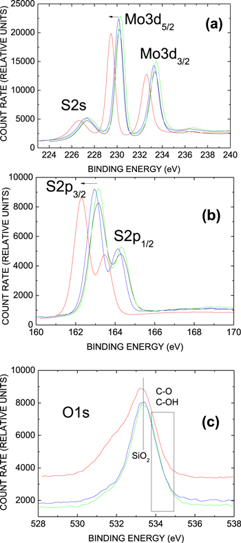
Figure 1. Mo3d (a), S2p (b), and O1s (c) XPS spectra (Al Kα excitation) from 2-ML thick MoS2 layers right after synthesis on sapphire (no transfer, black spectra), after transfer to 90 nm thick SiO2 and tape release at 140 °C (red spectra); after transfer and tape release at 140 °C and 15 min anneal in H2S (10 mbar) at 370 °C (blue spectra); and after transfer and tape release at 125 °C and 15 min anneal in H2S (10 mbar) at 370 °C (green spectra). Arrows indicate the direction of the transfer-induced binding energy shift.
Download figure:
Standard image High-resolution imageIn order to exclude the influence of x-ray induced charging effects caused by ionizing radiation in the oxide layer [36, 37], we used IPE that probes the interface potential barrier for electrons between the valence band top of MoS2 and the conduction band bottom of SiO2 in the most straightforward way [29, 30, 38]—a procedure not affected by the radiation-induced charges. Comparison of the electron IPE spectra from MoS2 directly-synthesized on SiO2 with those of MoS2 transferred onto identical SiO2 layers (figure 2) indicates a considerable increase of the IPE spectral threshold, with attendant weaker field dependence, after the transfer, which correlates with the XPS results. Apparently, the film transfer induces a stepwise electrostatic potential variation at the SiO2/MoS2 interface. Moreover, it is noticed that in some MoS2 samples transferred from sapphire, an even larger upshift of the IPE spectral threshold (up to ≈1 eV in some extreme cases as illustrated in figure 3) can be found near the sample edge despite the fact that Raman spectra (not shown) indicate good uniformity of the initial MoS2 film itself over a length scale of ≈5 cm. At the same time, simple coating of the MoS2 surface by PMMA (without bake) followed by removal in unheated acetone bath do not lead to any measurable variation of the IPE spectra. These observations point to the SiO2 surface as the possible source of changes in electrostatic potential occurring during MoS2 transfer.
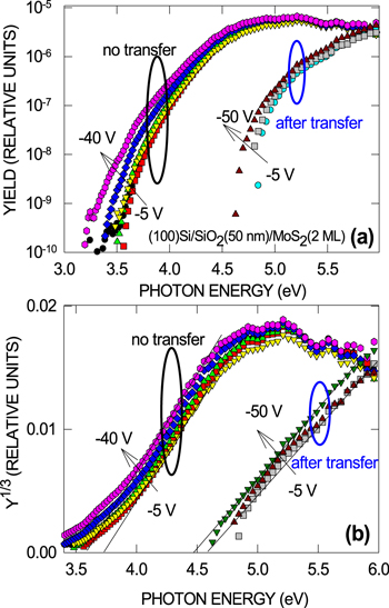
Figure 2. Semi-logarithmic (a) and Y1/3–hν spectral plots (b) of the photocurrent quantum yield measured in the indicated range of bias voltages applied to the thick Au contact pad on the (100)Si/SiO2(50 nm)/MoS2(2 ML) samples prepared by direct sulfurization of metallic Mo on top of SiO2 (no transfer) and after water-based transfer of an identically prepared MoS2 layer on top of another Si/SiO2 substrate.
Download figure:
Standard image High-resolution image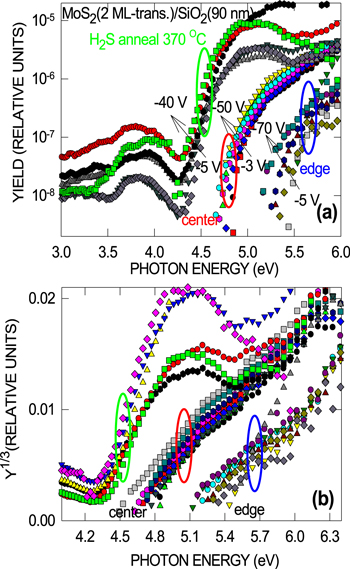
Figure 3. Semi-logarithmic (a) and Y1/3–hν spectral plots (b) of the photocurrent quantum yield measured in the center and near the edge of a (100)Si/SiO2(90 nm)/MoS2(2 ML) sample after transfer of MoS2 from sapphire on top of a SiO2 film, and after 15 min anneal in H2S (10 mbar) at 370 °C (center of the sample). The spectra are measured in the indicated range of bias voltages applied to the 100 nm thick Au contact pad.
Download figure:
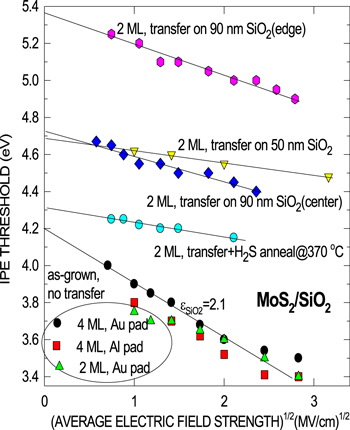
Standard image High-resolution imageIPE spectra taken from the samples subjected to the post-transfer annealing in H2S indicate the electron barrier to become somewhat lower (see figure 3), approaching its pre-transfer value (figure 2). However, the field dependence of the IPE spectra threshold remains much weaker than in the reference (no transfer) MoS2/SiO2 samples as can be seen from the Schottky plots shown in figure 4. This behavior may be explained by incorporation at the SiO2/MoS2 interface during MoS2 layer transfer of interface dipoles and/or negative charges that are partially 'repaired' during post-transfer annealing in H2S. Taking into account that the surface of SiO2 is exposed to air moisture with water molecules remaining at the oxide surface during thermal tape release (130 °C–140 °C), it may prove worth to address interactions of H2O with the oxide [39] as the possible reason of the electroneutrality violation at MoS2/SiO2 interface.
Figure 4. Schottky plot of the field-dependent electron IPE thresholds as measured on the as-grown reference (no transfer) MoS2/SiO2 samples and on those fabricated using layer transfer without and with subsequent annealing in H2S (15 min, 10 mbar, at 370 °C). Measurements are routinely done at the sample center; For the 2ML MoS2 layer without annealing, results from the sample edge are also shown for reasons of comparison. The bottom straight line shows the behavior expected for the ideal image-force barrier in SiO2 with the image force (optical) dielectric constant εSiO2 = 2.1.
Download figure:
Standard image High-resolution image
Silica surfaces in air are known to be covered by a layer of silanols (SiOH groups) of various geometries and water molecules [40]. These remain present even after transfer of a 2D-layer on top as is suggested to happen in the case of graphene on SiO2 [41]. Potentially, an array of polar O–H bonds in silanol groups with preferential orientation along the normal to the surface can form a dipole layer [42]. If assuming an effective charge transfer of 0.452 electron per H atom along the 0.12 nm long OH bond [42], the formation of a 1 eV dipole would require a SiOH entity density in the range of 1–4 nm−2, depending on the chosen static permittivity value (1 for vacuum or 3.9 for SiO2). This density agrees well with the density of silanols found at the silica surface varying from ca.3 to ca.0.8 nm−2 as the temperature increases from 200 °C to 700 °C [43], suggesting that silanols are realistic candidates to account for the interface barrier increase upon MoS2 layer transfer onto SiO2.
On the other hand, it is long known that water permeates into thermally grown SiO2 at relatively low temperature (<150 °C), leading to the formation of electron trapping centers [44, 45]. Both silanol (O3Si–OH) groups and interstitial water molecules have been identified as electron traps in SiO2 [46]. Trapping of electrons will result in a plane of negative charges which would 'pin' the top of the potential barrier at the MoS2/SiO2 interface, thus reducing its sensitivity to the externally applied electric field observed in the IPE spectra. Annealing in forming gas (N2 + 10%H2) at 400 °C eliminates the silanol groups due to reaction with atomic hydrogen generated at the metal/SiO2 interface [46] providing a technology-compatible process to restore the original oxide charge neutrality. However, since the application of forming gas anneal may lead to a sulfur loss from MoS2 [47], we used annealing in H2S instead. This processing is thought to be capable of 'repairing' both possible S-deficiency in MoS2 and remove silanols from the oxide surface. The annealing temperature of 370 °C was chosen to ensure thermal desorption of water and other adsorbates from the sample surface but still within the typical 'back-end-of-the-line' thermal budget. Indeed, upon such treatment, the IPE threshold shifts back towards the ≈4–4.2 eV range. However, the threshold field dependence is still much weaker than that in control (no transfer) samples (also shown in figure 4) suggesting that not all negative charges are removed from the MoS2/SiO2 interface.
In order to distinguish between barrier height modifying contributions from interface dipole and interface charges, we conducted electrical conductivity measurements on MoS2 layers using backside gating. The current–voltage curves shown in the Supporting Information for the MoS2 films transferred on 90 nm thick SiO2 layer can be compared to the previously reported results for the case of directly-synthesized MoS2 on SiO2 [16], revealing the absence of any significant shift along the backside gate voltage (Vg) axis. At the same time, these measurements affirm good lateral uniformity of the transferred MoS2 layer at the length scale of several cm, which supports the earlier conclusion that the macroscopic inhomogeneity of the interface barrier (figure 3) is probably related to the surface of the SiO2 underlayer. On this basis we suggest that an interface dipole rather than a net charge in SiO2 is responsible for the interface barrier changes upon transfer of MoS2 layers on SiO2.
More detailed electrical analysis of back-gated sulfurization-grown MoS2 transistors as well as patterned structures used in the transfer-line method (TLM) has been presented in earlier publications [29, 32, 33]. The results indicate that the electron mobility increases from ≈ 0.2 cm2 V−1 s−1 in layers synthesized at 800 °C on SiO2 to ≈ 3 cm2 V−1 s−1 in layers grown at 1000 °C on sapphire (see table 1 in [29]) which is ascribed to better crystallinity of MoS2. At the lower end, these values are comparable to those reported for single-crystal bi-layer MoS2 flakes obtained by defoliation if probed in air (0.12 cm2 V−1 s−1) [48] and to the mobilities of <0.1 cm2 V−1 s−1 reported for large-area MoS2 films prepared by similar metal sulfurization process [49]. Removal of adsorbates from un-encapsulated MoS2 flakes in vacuum leads to significant mobility improvement [48, 50] but it remains well below the theoretical estimate of ≈410 cm2 V−1 s−1[51]. In line with these observations is the significant improvement of electron mobility (up to 12 cm2 V−1 s−1) observed in the sulfurization-grown MoS2 layers studied in this work upon post-transfer capping by chemical-vapor deposited (CVD) SiO2 [28] which can also be a result of the Si-OH group removal effect due to atomic hydrogen release during the oxide CVD. Similar mobility values, close to 10 cm2 V−1 s−1 for 1 ML and to 20 cm2 V−1 s−1 for a bi-layer MoS2, were recently reported for the films grown by CVD from ther Mo(CO)6 precursor [52].
It is also noticed that Ni/MoS2 contact resistance (Rc) values measured in TLM structures are sensitive to the air and water exposure [28]. Typical values of Rc for the studied sulfurization-grown MoS2 films transferred onto SiO2 are in the range 25–100 kΩ μm with a trend to increase at low back gate voltage (see upper inset in figure 3(a) in [33]). This behavior may be explained by the formation of a depletion layer in n-type MoS2 due to the considerable (≈1 eV) barrier between the Fermi level of Ni (3.7 eV below the CB bottom of SiO2, see table 1 in [53]) and the CB of the sulfurization-grown MoS2, see band diagram shown in figure 5(b) in [30].
4. Discussion and conclusions
The revealed violation of electroneutrality of the MoS2/SiO2 interface upon layer transfer processing may have a significant impact on electron transport in the MoS2 film because the dipole potential of polar silanol groups may result in additional carrier scattering. The high density of these scattering centers, in the order of ≈1 nm2 as suggested by the observed electron barrier changes, may explain the inferior transport properties of 2D films transferred on SiO2 as compared to other substrate materials such as BN [27]. Though the beneficial effect of the post-transfer anneal in H2S (at 370 °C) is obvious, the anneal temperature should probably be increased to facilitate more efficient silanol removal. This, however, might cause a problem if non-sulfide materials, such as graphene, are used in the 2D stack since theyse can be damaged during anneal [54]. It is also worth of adding here that similar violation of interface electroneutrality can also be expected in the case of the ink-printing approach to 2D-heterojunction device fabrication [55]. In other words, not only stability of the transferred 2D semiconductor layer matters but, also, that of the target substrate as well. To resolve this issue, non-oxide substrates with more stable surfaces might help to maintain the electrostatic neutrality.
In conclusion, experiments reveal significant, up to ≈1 eV, interface barrier changes caused by transfer of MoS2 layers onto thermally grown SiO2. The results suggest that the formation of an interface dipole layer is responsible for the observed barrier instability which is tentatively associated with the presence of silanol groups at the surface of the SiO2 layer below the MoS2 film. Post-transfer annealing in H2S appears to be useful in reducing the interface barrier perturbation suggesting that electroneutrality of the interface is restored at least partially.
Acknowledgments
This work was supported by the Flanders Innovation & Entrepreneurship [2Dfun (2D functional MX2/graphene hetero-structures), an ERA-NET project in the framework of the EU Graphene Flagship] and by the KU Leuven Internal Fund (project C14/16/061).