
Abstract
We report on structural, compositional, and thermal characterization of self-assembled in-plane epitaxial Si1−xGex alloy nanowires grown by molecular beam epitaxy on Si (001) substrates. The thermal properties were studied by means of scanning thermal microscopy (SThM), while the microstructural characteristics, the spatial distribution of the elemental composition of the alloy nanowires and the sample surface were investigated by transmission electron microscopy and energy dispersive x-ray microanalysis. We provide new insights regarding the morphology of the in-plane nanostructures, their size-dependent gradient chemical composition, and the formation of a 5 nm thick wetting layer on the Si substrate surface. In addition, we directly probe heat transfer between a heated scanning probe sensor and Si1−xGex alloy nanowires of different morphological characteristics and we quantify their thermal resistance variations. We correlate the variations of the thermal signal to the dependence of the heat spreading with the cross-sectional geometry of the nanowires using finite element method simulations. With this method we determine the thermal conductivity of the nanowires with values in the range of 2–3 W m−1 K−1. These results provide valuable information in growth processes and show the great capability of the SThM technique in ambient environment for nanoscale thermal studies, otherwise not possible using conventional techniques.
Export citation and abstract BibTeX RIS

Original content from this work may be used under the terms of the Creative Commons Attribution 3.0 licence. Any further distribution of this work must maintain attribution to the author(s) and the title of the work, journal citation and DOI.
1. Introduction
One-dimensional Si1−xGex semiconductor nanostructures have attracted enormous research interest due to their unique electronic properties and recently have been utilized in a wide range of applications, such as heterojunction bipolar transistors, strained Si complementary metal-oxide-semiconductor (CMOS) devices [1, 2] nanoelectronics [2–5] and IR sensors [6]. Nanowire transistors with gate lengths of 5 nm have been produced in gate-all around configuration by scaling down the corresponding intrinsic nanowires (NWs) channel body [7, 8]. The continuous downscaling of semiconductor devices results in the fabrication of devices with sub-micrometer feature sizes, where localized Joule heating becomes important. The performance and the reliability of these devices are strongly connected to the efficient control of the thermal transport, thus, there is a need for a better understanding of the heat transfer mechanisms at the nanoscale. Towards this direction, new measurement techniques have been developed to characterize thermally sub-micrometer features [9], while the key fabrication challenge to align and grow bottom-up NWs into complex patterns or structures still remains.
Recent studies reported new approaches to grow NWs with in-plane geometries into desired areas and along precise directions. The fabrication processes are performed either on metal substrates in arrays without using templates and catalysts [10, 11], or on semiconductor substrates [11–15] by adjusting the location of catalysts, offering the possibility of in situ fabrication of nanowire-based devices. In particular, in-plane assembled nanostructures target suitable geometry for integration on Si chips and CMOS architecture using planar microfabrication technology [16]. The composition analysis of this kind of nanostructures is usually performed by micro-Raman spectroscopy [15, 17–19] and energy dispersive x-ray (EDX) analysis [20, 21]. Although Raman spectroscopy is a fast and non-destructive technique to characterize nanostructures, there are some limitations, such as the lateral spatial resolution of about 300 nm, which does not allow discriminating composition inhomogeneities within, e.g. sub-300 nm nanostructures.
Thermal transport in Si1−xGex NWs has been studied over the last decade both theoretically [22–29] and experimentally [25–28, 30, 31]. Most experimental studies focused on measuring the thermal conductivity of individual Si1−xGex NWs with various Ge concentrations and diameters using microfabricated suspended thermometer/heater platforms. Furthermore, recent studies even proved the existence of ballistic thermal conduction in Si1−xGex NWs with low thermal conductivity for a wide range of structural variations and alloy concentrations [32]. These results showed the significant potential of Si1−xGex NWs in thermoelectric applications. However, only few experimental studies have reported thermal transport on supported Si1−xGex NWs or NWs embedded in a matrix material [33, 34], which are more representative structures for many future NW-based applications. Here we report first a thorough investigation of structural, morphological and chemical properties of in-plane epitaxial Si1−xGex alloy NWs by using high resolution transmission electron microscopy (TEM) measurements and EDX spectroscopy. Then, we report thermal transport results from the supported NWs using scanning thermal microscopy (SThM), by probing heat flux related signals between a heated scanning probe sensor and the investigated materials in contact with it. We estimate the dominant thermal resistive components contributing to the SThM signals during the heat exchange of the probe with the investigated nanostructures using finite element method (FEM) simulations and an analytical heat-spreading model, which allow us to determine the thermal conductivity of the NWs.
2. Materials and methods
2.1. Fabrication
The in-plane epitaxial Si1−xGex alloy NWs were grown by molecular beam epitaxy (MBE) on a Si (001) substrate using Au nanoparticles as catalyst. The growth method consists of a three-step process involving the deposition of 1 nm thick each Au and Si layers, the AuSi seeds formation by annealing these layers at 800 °C and, finally, the formation of the Si1−xGex alloy by continuously supplying a Ge flux at 550 °C. More details about the fabrication process can be found elsewhere [13].
2.2. Morphology and composition
The sample surface was characterized ex situ by scanning electron microscopy (SEM) and atomic force microscopy (AFM), using a Quanta-200 ESEM-FEG and a MultiView SPM 4000 system from Nanonics, respectively. Then the cross-sectional morphology of Si1−xGex NWs was investigated using an Analytical Titan Low-base system in TEM and STEM modes. Ultra-high resolution images in scanning-transmission mode (HR-STEM) were also obtained. The elemental composition of the Si1−xGex alloy NWs and the substrate surface in a cross sectional plane was analysed using EDX elemental mapping, which provided spatially resolved chemical composition variations within individual NWs and the substrate surface with 1 nm spatial resolution. A dual beam focused ion beam (FIB) (Dual Beam Helios 650 model) was used to prepare cross sections of specific NWs for TEM imaging by standard TEM lamella preparation [35].
2.3. Thermal analysis
The thermal measurements were performed using SThM in ambient environment (MultiView 4000 System, Nanonics). Our system is a multi-probe scanning probe microscopy (SPM) system, with an open architecture which allows flexible integration of different analytical tools. A platinum (Pt) dual wire resistive thermal probe in active mode was used for the thermal characterization by applying high constant currents through the probe resistor to induce Joule heating. The thermal probe, which in this case is being used as the heater and thermometer, consists of two Pt wires stretched through a glass nanopipette (borosilicate glass) and fused together at their ends, creating a heating junction source. The mechanical interaction between the tip and the surface is controlled using a tuning fork in normal force mode with phase feedback, therefore, avoiding the laser-induced heating of the probe found in standard optical-based feedback systems. The principle of operation of SThM is based on the dependence of the electrical resistivity  on temperature (T), where the change in the electrical resistance is measured as a change in the output voltage
  across a Wheatstone bridge circuit. Therefore, changes in heat flux are monitored through the change of the probe resistance. More details regarding the experimental set-up and probe specifications can be found in the supporting information (SI) is available online at stacks.iop.org/NANO/28/505704/mmedia.
3. Results and discussion
3.1. Morphology and composition
The surface morphology of the Si1−xGex alloy NWs was characterized by means of SEM, AFM and TEM. AFM images and topography profiles of the NW samples can be found in the SI. Figure 1(a) shows the SEM image of the AuSi clusters after annealing the 1 nm Au and Si films at 800 °C. A SEM image of as grown Si1−xGex alloy NWs is presented in figure 1(b), where the variation of widths, heights and lengths is evident as well as the directional growth along the 〈110〉 directions of the Si substrate. The width and length distribution of these NWs was measured to be  and
and  respectively.
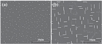
Figure 1. SEM images of (a) the AuSi seeds after 5 min annealing of the Au and Si layers at 800 °C and (b) the in plane epitaxial Si1−xGex alloy NWs after the Ge deposition by MBE.
Download figure:
Standard image High-resolution imageDue to the excess Au content of the liquid SiGeAu droplets, Au rich particles at the end of the NWs are apparent after the MBE growth. These nanoparticles usually match the transversal size of the NWs, indicating that growth takes place following a vapour–liquid–solid (VLS) mechanism from the continuous supply of Ge flux at a fixed temperature of 550 °C. Previous investigations showed that at this temperature the diffusion length of Si atoms on the surface is quite small whereas for Ge atoms it is of the order of  [15]. Initially, Ge atoms as supplied from the effusion cell are homogeneously distributed on the whole substrate surface. All atoms remain adsorbed (the sticking coefficient at 550 °C is 1 [36]) and diffuse before they incorporate to the growing nanostructures. Most Ge atoms are preferentially collected by the liquid droplets and contribute to the NWs growth.
Therefore, the fraction of atoms that does not reach a droplet must contribute to form a thin wetting layer (WL) on most of the substrate. Here, the term WL is used to denote rather planar growth morphology although its final characteristics are certainly influenced by the presence of Au. The existence of this WL could not be previously detected and is observed in the present work. The composition of individual NWs was found uniform along the length and non-uniform along the vertical cross section [13]. Even if the SiGe composition given by the VLS process should be well determined, the behaviour of the diffusing Ge atoms obviously can modify both the average composition as well as the vertical composition profile, as is evaluated in this work.
The cross-sectional morphology and the chemical composition variations were investigated in four NWs of different dimensions by means of TEM-EDX. Figure 2 displays TEM images of the four Si1−xGex alloy NWs with decreasing width. From the TEM analysis, we found that the NWs have elongated shape, with the height (h) roughly decreasing proportionally to the width (w) according to a relation  where
where  This approximate geometrical relationship is related to the fact that the NWs are actually faceted with a {001} top facet and lateral sidewalls mostly consistent with {115} planes. The inclination of these planes is Ө = 15.8°. Most of the width is given by the lateral sidewall geometry, that is, the proportionality constant α is larger but close to (tan Ө)/2 = 0.14. In addition, we found that the NWs are partially buried with approximately half of the thickness embedded in the substrate. In fact, the NWs start to nucleate from droplets forming at dissolution pits. It was found that the droplets dissolve the substrate generating truncated inverted pyramids, with their lateral sides always oriented along 〈110〉 directions of the substrate and sidewalls consistent with {115} planes, resulting in the approximate mirror-like appearance of the cross section and the preferential elongation direction of the NWs. Although the growth mode in these samples is not a purely epitaxial process of SiGe on Si, cross-sectional HR-STEM (see details in the SI) showed crystallinity and substrate dependent crystallographic orientation.

Figure 2. (a)–(d) Cross-section TEM images of the four investigated Si1−xGex alloy NWs. Note that the scale bar is different in each image.
Download figure:
Standard image High-resolution imageTable 1 summarizes the morphological characteristics of the four selected NWs. The perimeter/area ratio (P/A) accounts for the surface to volume ratio of the NWs. For the same NWs, we present in the next section SThM measurements which were performed before the composition analysis.
Table 1. Morphological characteristics of the four investigated Si1−xGex alloy NWs. The values inside the brackets represent the error of the measurement.
| Si1−xGex | Width (nm) | Height (nm) | Length (μm) | P/A (μm−1) |
|---|---|---|---|---|
| NW1 | 130 (5) | 20(5) | 1.30 (0.05) | 0.14 (0.01) |
| NW2 | 225 (5) | 47(5) | 1.35 (0.05) | 0.057 (0.01) |
| NW3 | 420 (5) | 82(5) | 2.05 (0.05) | 0.032 (0.01) |
| NW4 | 585 (5) | 105(5) | 1.20 (0.05) | 0.023 (0.01) |
Having discussed the morphology of the NWs, we move to the chemical composition analysis of the sample. EDX spectra and elemental chemical maps revealed the existence of Si, Ge and Au both on the sample surface and inside the NWs in different concentrations. Figure 3(a) shows a cross-section TEM image in a flat region free of NWs of the sample surface, where the 5 nm WL is apparent. The rectangular box marks the selected region where the composition analysis was conducted. Figures 3(b), (c) illustrate the composition map of the WL and the corresponding 2D composition profile, respectively, showing clear evidence of an alloyed WL with continuous distribution of Si and Ge and trace amounts of Au. Different areas of the WL were analysed in order to confirm its homogeneity in the whole substrate surface. Figure 3(d) illustrates the composition profile obtained from the composition map by averaging in the lateral direction from the surface into the substrate. Particularly, within the WL we found a vertical alloy composition gradient with a maximal Ge composition of 14.5 at% at the surface uppermost. The relative low Ge concentration on the WL indicates that Ge diffusion on the substrate towards the NW positions is very effective.

Figure 3. (a) TEM image of the sample surface where a 5 nm WL is formed, (b), (c) the corresponding composition map and composition profile, respectively, and (d) the average Si, Ge and Au concentration in depth. The spatial resolution of the EDX system is 1 nm.
Download figure:
Standard image High-resolution imageWith regard to the composition maps and composition line scans obtained in the selected NWs, we found different vertical composition gradients depending on the NWs cross-section. As the latter decreases, the composition gradient becomes larger. Figure 4(a) illustrates the average atomic Si and Ge concentration of each NW as a function of its height. The composition profiles were obtained from composition maps throughout the NWs in the central region around the maximum height. The selected nanowire regions and the corresponding composition maps are shown in figure 4(c) (dark colour means absence of material). The average atomic Ge composition increases (from 50% to 82%) as the width of the NWs decreases (from 585 to 130 nm). The existence of these composition gradients was expected due to the diffusive nature of the growth mechanism, as has been discussed in previous reports [13, 15], but the precise values of composition in the NWs core region were difficult to estimate by micro-Raman imaging [15].
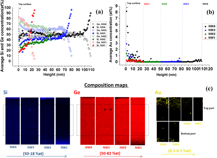
Figure 4. Average (a) Si, Ge and (b) Au concentration as a function of the height of the four supported Si1−xGex alloy NWs, and (c) the corresponding composition maps.
Download figure:
Standard image High-resolution imageAlthough it was not possible to discern the cross section dimensions of the NWs in the previous micro-Raman investigations, it was inferred that, in average, thinner NWs were richer in Ge, as is clearly shown here. The different vertical composition gradients most likely corroborate that diffusing Ge atoms on the substrate tend to incorporate preferentially at regions closer to the top of the NWs, giving the relative Ge concentration increase, which is larger in thin NWs. While the agreement with previous micro-Raman investigations is only qualitative, the results presented here also show that the uppermost regions of the NWs tend to be Ge-richer than the core and lowermost regions.
In addition, we found embedded clusters of Au within all the NWs volume, which indicates that the Au catalyst material was incorporated into the NWs during the growth process. The average atomic Au concentration decreases (from 8.5% to 0.5%) as the width of the NWs decreases. Figure 4(b) shows the depth dependent average Au concentration for the four selected NWs. From the composition maps which are shown in figure 4(c), we found that the Au is mostly concentrated on the top part of the volume of the NWs. The precise determination of the Au concentration and distribution in the NWs is crucial, as the incorporation of the material catalyst within the NWs volume might affect their electrical properties by creating deep traps in the band gap and changing the carrier mobility as has been discussed elsewhere [37].
3.2. Thermal properties
In this section, we present and discuss the study of the thermal transport across Si1−xGex alloy NWs of different morphological characteristics performed with the tip of a SThM. Sensitive probing of tip-sample effective thermal conductance or resistance variations was conducted by monitoring changes in heat flux related signals by the change of the probe electrical resistance. We consider the heated contact area as an isothermal circular heat source of radius rc = (50 ± 2) nm, as determined from SEM, whereas the low heat capacity (Cp = 133 kJ kg−1 K−1) of the Pt wires makes the probe sensitive to thermal variations. Figures 5(a), (b) show SEM images of the cantilever where the heating Pt elements are exposed through a glass pipette, and a closer view of the Pt junction, respectively. The thermal probe was used in the active SThM mode, where the probe resistive element is heated by the Joule effect. The thermal conductance between the thermal probe and the sample  includes contributions due to radiation, the liquid meniscus and air, in addition to its dependence on the contact area [38–43]. Radiative heat transfer is generally assumed to be negligible as compared to the other mechanisms [41]. The values of the thermal conductance through the water meniscus have been found to be a few percent of the total contact thermal conductance [44]. Therefore, the thermal contact conductance is mainly dominated by the solid–solid contact and air conduction. Regardless of which of these two mechanisms dominate, the heat conduction through the air is independent of the surface material [45]. Moreover, since the measurements were performed in regions of smooth topography, we do not expect significant variations of the air heat transfer related to changes in the air gap between the tip and the sample surface.

Figure 5. SEM images of (a) the SThM probe with the integrated Pt resistive elements and (b) the nanometer-scale junction in the Pt wires.
Download figure:
Standard image High-resolution imageFirst, we obtained the 2D topography and thermal images of the NWs with different dimensions by simultaneous mapping the local variations in height (figure 6(a)) and tip-sample thermal resistance (figure 6(b)). The images consist of 256 × 256 points. The integration time of about 30 ms at each point was long enough for the heated volume to reach thermal equilibrium. It is worth mentioning that the scanning probe environment was kept under well controlled conditions (ambient temperature and humidity). In the thermal image (see figure 6(b)), the darker regions correspond to signals acquired by the tip in contact with only the Si1−xGex NWs, and the brighter regions corresponds to areas where the scanning probe tip is in contact with the WL. In high thermally conductive regions, the increased heat flux from the tip to the sample results in a larger temperature drop of the probe at the heated junction, which, in turn, results in a lower probe electrical resistance  A Wheatstone bridge circuit was used to correlate changes of
  with the measured direct output voltage
  In our configuration, changes in the probe electrical resistance
  produce proportional changes of the output voltage
  (see details in the SI).
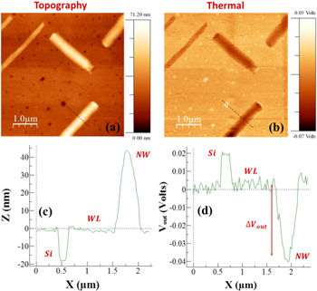
Figure 6. Examples of (a) topography and (b) thermal image of Si1−xGex alloy NWs with different dimensions. (c) Topography and (d) thermal signal profiles along the dashed lines in figures 6(a) and (b), respectively.
Download figure:
Standard image High-resolution imageBefore each thermal scan, the bridge was balanced with the probe in contact with the WL  We then proceed to scan the sample surface and measured the off-balance bridge signal, i.e., the relative changes of the SThM signal
  compared to the reference value in the WL. This procedure ensures an increased thermal image contrast and an accurate monitor of any signal variation. The relative variation of the thermal signal between the WL and a single NW can be directly observed in the thermal profile of figure 6(d), which is obtained from the line scan of the thermal image (dashed line in figure 6(b)). The 40 mV drop of the output voltage on top of the NW compared to the WL region indicates a drop of the heat conduction from the probe to the sample, i.e., an increase of the probe-sample thermal resistance.
Note that the probe-sample thermal resistance is composed of interfacial (Kapitza) thermal resistance and the spreading thermal resistance in the NW and the underlying Si substrate. For the four selected NWs, we found that the absolute value of the relative change of the SThM signal  varies from −10 to −56 mV with increasing cross-sectional size of the NWs. Finally, the absolute thermal signals in the NWs are obtained taking into account the absolute response of the probe in the WL
  The absolute response of the probe in the WL
  was measured by balancing the bridge far away from the sample surface and then bringing the probe in contact with the WL. The surface topography indicates the presence of square-like regions where the WL vanishes leaving holes of uncovered Si substrate. The thermal profile in the uncovered Si (see figure 6(d)) displays an increase of the output voltage
  which is consistent with an increased heat transfer compared to the WL. However, in non-contacting regions (<100 nm), such as the Au particles in the NWs and few anti-dots in the WL (figure 6(b)), the thermal contrast appears to be dominated by the topography related changes of the tip-sample contact geometry. Consequently, we measured mean values of the thermal response of the probe in different NWs by taking into account only the thermal signals derived from flat regions where topography induced artifacts were not apparent.
Before we analyse the thermal response of our probe in the four Si1−xGex NWs and in the WL, we describe and estimate the thermal resistive components, which contribute to the SThM signals during the thermal exchange of the thermal probe with the sample surface. Although the effect of heat transfer in the ballistic regime might be considerable at length scales comparable to phonon mean free paths (MFPs) of the probe and the sample material, here we assume the thermal transport as entirely diffusive. This assumption is justified as long as the system is in the steady state and the phonon MFPs in the NWs is smaller than the contact area of the probe. This assumption will be validated later when comparing the experimental data and the results obtained using FEM simulations in the diffusive regime.
The measured heat flux is considered as a function of different thermal resistances, such as the thermal resistance of the probe in air environment  the thermal interface resistance between the probe and materials in contact (thermal contact resistance)
  and the thermal spreading resistance within the sample
  that includes both NWs and underlying substrate (see figure 7). Note that the contribution of the interface resistance between the SiGe NWs and the bottom Si substrate
  is discussed later in this article.

Figure 7. Schematic of the nanoscopic tip-sample contact and the equivalent thermal resistance circuit.
Download figure:
Standard image High-resolution imageTherefore, we divide the total Joule heat generated by the current flowing through the sensor  into two pathways,
  where
where 
 are heat fluxes transferred from the probe tip to the sample and to the probe base, respectively. The equivalent thermal resistance
  is given as follows [42, 46]:
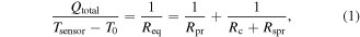
where  is the heater temperature, and
  is the ambient temperature. We determine each thermal resistance contribution to
  using FEM simulations (COMSOL Multiphysics) and analytical models reported elsewhere [43, 47, 48]. The full procedure is described in detail in the SI. FEM simulations were also used to calculate the temperature distribution in the thermal probe, taking into account the heat transfer from the probe to the surrounding air, and determine
  The value provided by the FEM model was
  = 1.7 × 10⁶ KW−1.
Since the WL is homogeneously formed on the Si substrate we can estimate the spreading resistance when the thermal probe is in contact with the WL,  from the analytical thin-film approximation derived by Dryden [48]. This model describes the spreading of heat from a circular heat source into an isotropic structure in the case that the thickness of the film is significantly smaller than the contact radius of the heat source. The obtained value
  = 5.32 × 10⁵ KW−1 is one order of magnitude larger than the spreading resistance in bulk Si (Rspr(Si) = 3.37 × 10⁴ KW−1) due to the lower thermal conductivity of the SiGe alloy film forming the WL.
The magnitude of  in the NWs is expected to vary with both, the geometrical scaling of the NWs and with possible variations of the thermal conductivity between NWs. We estimated the thermal spreading resistance variations at the probe-NWs contacts (Rspr(NWs)) first by following the same analytical film approximation for the spreading resistance [48]. Assuming a perfect thermal contact between the thermal tip and the NWs, we estimated thermal spreading resistance variations from 6.0 × 10⁵ to 3.9 × 10⁶ KW−1 in a thermal conductivity range from 1 to 5 W m−1 K−1. In order to validate the estimations of
  obtained from the thin film approximation, we performed FEM simulations to compute the thermal spreading resistance variations in the four investigated NWs taking into account their real morphology
  This procedure gave values of
  in the range 4.3 × 10⁵– 4.4 × 10⁶ KW−1, similar to that derived from the analytical model.
Finally, the value of  which represents the thermal resistance at the probe-sample interface, was estimated to be 9.3 × 10⁷ KW−1 both in the WL and the NWs. Despite the relatively high value of
  which limits the sensitivity of the method, it does not prevent the detection of small amplitude signal changes related to
  variations (see figure S7 in the SI). The determination of
  was possible by combining our experimental data and the calculated thermal spreading resistance variations between the WL, the NWs and the bulk Si (see details in the SI). Nevertheless, we would expect
  in the NWs and the WL to be similar since the two materials in contact were the same (Pt/SiGe contacts) during the thermal measurements and the amplitude of the contact force was kept approximately constant.
Following the identification of the heat transfer mechanisms between the thermal probe and the sample, as well as their relative weight, we discuss the variations observed in the SThM signal between different NWs. Considering that the probe Joule power dissipated into the sample is proportional to  we correlate changes in
  with variations of the effective thermal conductance
  between our heated tip and the sample surface (see details in the SI). The relation between the measured
  and the estimated thermal resistances is expressed by the ratio (g) defined as follows:
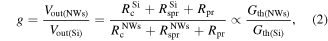
where Vout(NWs) and Vout(Si) represent the absolute thermal signals obtained on the Si1−xGex NWs and the bulk Si, respectively. Figure 8 shows the ratio g (black spheres) obtained from the four investigated NWs, as a function of their surface to volume ratio. The observed trend reveals that the effective thermal conductance between the heated tip and the NWs  which scales proportional with the ratio g, increases in NWs with larger surface to volume ratio. Figure 8 also shows the effect of the 5 nm SiGe alloy WL on the SThM signal compared to the thermal signal measured in bulk Si. In the same graph, we have plotted the normalized thermal response of the probe
  obtained from the thermal spreading resistance values
  which were calculated for each NW for values of the thermal conductivity of k = 2 and k = 3 W m−1 K−1 (red and green stars in figure 8).

Figure 8. Plot of the experimental thermal ratio (g) (black spheres) and the ratio obtained from the FEM simulations (gFEM) (red and green stars) versus the surface to volume ratio of the Si1−xGex NWs.
Download figure:
Standard image High-resolution image
Based on the spreading resistance diffusive model, the obtained trend of increasing g ratio, i.e., thermal conductance increase with increasing NW cross-section, is attributed to the increasingly dissipated heat to the substrate, owing to the larger thermal conductivity of Si. The comparison in figure 8 shows a quantitative agreement between the FEM simulations, which take into account only  variations, and our experimental results, confirming that, despite
  is the dominant resistive component, the variations in the thermal response of the probe due to different NWs are associated with variations in
  Further details on the comparison of the estimated variations of
  and
and  can be found in the SI (figure S6). The experimental data fall between the two calculations for k = 2 and k = 3 W m−1 K−1, with values for NW3 and NW4 closer to the k = 2 W m−1 K−1. These small deviations between the modelling and the experimental data can be attributed to composition variations in the NWs, which were not taken into account in the FEM simulations (e.g. presence of Au and SiGe composition).
Recalling the results from the composition analysis (figure 4(b)), it is interesting to note that NW3 and NW4 showed the highest Au concentration. The increased Au concentration in these cases generates a nanoscale disorder in the SiGe lattice, which increases the number of phonon scattering events. We consider the concentrated Au atoms as an additional thermal resistive layer, which potentially reduces the average phonon MFPs in the NWs and further suppresses the heat dissipation perpendicular to the substrate. Recently, interfaces of different types have been reported to provide enhanced phonon scattering and phonon trapping at localized vibrational modes [49–53]. Moreover this mechanism can effectively suppress the transport of long-wavelength phonons and, therefore, the ballistic transport.
Refining the values of the thermal conductivity in the previous analysis, by better matching the calculated  to the experimental g value, we could estimate the thermal conductivity of NW3 and NW4 to be 2.2 ± 0.3 W m−1 K−1 and of NW1 and NW2 to be 2.7 ± 0.3 W m−1 K−1, which are values almost four times lower than the bulk value [50]. This range is similar to the values expected in SiGe nanostructures of similar characteristic size and composition, where the reduction of the thermal conductivity has been attributed to phonon boundary scattering [30, 31, 54–56]. More importantly, our analysis indicates that even for nanometer scale heat sources and low conductive materials, heat dissipation can be consistently explained with a diffusive thermal spreading model.
Finally, in order to assess the effect of an interfacial thermal resistance, rint between the NWs and the substrate, we used an extension of the thin film approximation model, which accounts for the effect of an interface on the thermal spreading resistance [57]. Since the precise knowledge of  is difficult in the present samples, we used a wide range of values comprising those reported in SiGe based structures [49, 58, 59] and investigated its effect on the
  ratio. Values of interfacial thermal resistance between 0 and 1 × 10⁻⁸ m2 KW−1 were chosen and set in the analytical modelling. As expected, by introducing an interfacial thermal resistance the ratio g decreased. The variations were larger with decreasing NW height in the order of a 0.1%–0.6% for NW4 and NW1, respectively, for a value of the thermal interface resistance of 1 × 10⁻⁸ m2 KW−1. These differences are within the experimental error and do not affect the values of the thermal conductivity of the NWs given previously. Moreover, a decreasing g ratio with increasing rint supports the explanation in which the variations of the data with respect the model are more likely due to Ge composition variations and Au content.
4. Conclusions
In conclusion, we have performed a comprehensive experimental study of the structure and the composition of supported in-plane epitaxial Si1−xGex alloy NWs of different dimensions, which provides a deeper understanding of the bottom-up growth processes. We have presented new evidences regarding the morphology of the NWs, their size-dependent gradient composition and the formation of a 5 nm thick WL on the substrate surface. In addition, we have studied the thermal transport between the heated tip of a SThM and the sample surface. SThM has provided high resolution thermal contrast images of sub-micrometer structures on the sample surface with 100 nm lateral thermal resolution. By estimating all the major thermal resistive components contributing to the SThM signal at the probe-sample contact and determining the dominant mechanisms, we have been able to analyse the experimental thermal response. Particularly in the NWs, we found that the heat flux related signal are determined by thermal spreading resistance variations, revealing the relation between the measured SThM signal and the effective thermal conductance. The results obtained using FEM simulations, which are in good agreement with the experimental results, allowed us to determine a range of thermal conductivities (2–3 W m−1 K−1) for the investigated NWs. These results can provide essential guidance for the integration of epitaxial in-plane NWs in devices with varying composition in a controllable way and with improved heat management.
Acknowledgments
The authors acknowledge the financial support from the EU FP7 project Quantiheat (Grant No 604668), the Spanish MINECO projects NanoTHERM (Grant No. CSD2010-589 0044) and PHENTOM (FIS2015-70862-P) and the program Severo Ochoa (Grants SEV-2013-0295 and SEV-2015-0496). ICN2 acknowledges funding from the CERCA Programme/Generalitat de Catalunya. We would like also to thank A Ruiz and M Alonso for the preparation of the Au films used as substrates, and M Papandreou for the graphic illustrations.