

Abstract
In this paper, a broadband non-destructive and non-contact local characterization of graphene fabricated by epitaxial method on silicon carbide is demonstrated by using an interferometer-based near-field microwave microscope. First, a method has been proposed to extract the dielectric properties of silicon carbide, and finally, the graphene flake has been characterized as a resistance (∼20 kΩ) and a small inductance (360 pH) in the frequency band (2–18 GHz). The advantage of the proposed method is that there is no need to fabricate electrodes on the sample surface for the characterization. The instrument proposed is a good candidate for the local characterization of 2D materials.
Export citation and abstract BibTeX RIS
1. Introduction
Near-field microwave microscopy (NFMM) has been successfully applied to the characterization of various kinds of materials such as dielectrics, semiconductors and metals [1, 2]. This technique generally uses a waveguide or a probe to generate evanescent microwaves in order to investigate the local properties of materials [3]. Since recently, it has advanced to near-field quantitative material characterization with nanometric resolution [4, 5]. In addition, compared with dc probes, additional fabrication of contact electrodes are not required when using NFMM, which allows non-contact and non-destructive evaluations of materials/structures [6].
In recent years, two-dimensional nanomaterials such as graphene have attracted significant attention from the scientific community because of their unique physical properties [7, 8]. Graphene-based devices/structures have been investigated for numerous applications of high-speed electronics such as for example digital electronics and RF analog devices [7–10]. For the realization of these devices, the characteristics of graphene have to be carefully evaluated. So far, the electronic properties of graphene have been mostly investigated in dc or low frequency range by techniques such as the transmission line method (TLM) and probing methods [11, 12]. The coplanar waveguide (CPW) method has also been applied to evaluate the surface impedance of single layer graphene [13]. However, these characterization methods require additional electrodes fabrication process which could degrade the electrical properties of the samples. Furthermore, most of these methods such as the TLM and CPW approaches are not convenient and not efficient to investigate local properties of materials, which is quite an issue for testing inhomogeneous samples. So, there is an urgent need for the development of a non-destructive and non-contact characterization tool with a good spatial resolution compatible with this kind of evaluation.
Driven by the great interest of graphene devices in high frequency range applications, the NFMM has already been effectively employed for non-destructive quantitative imaging of the local impedance of monolayer and multilayer graphene [6, 14]. Thanks to the use of probe–sample capacitive coupling and a relatively high frequency of a few GHz, this method allows investigating the high frequency properties of materials, with a nanometric scale spatial resolution without a dedicated electrode. However, as most of these NFMMs are resonator-or quarter wavelength transmission line-based, their working frequency range is limited. So, a big challenge for the NFMM is to perform wideband measurement with high sensitivity [15]. In addition, most NFMMs are working in contact mode hence there is a risk of scratching the sample by the probe tip.
Thus, in this work, a home-made NFMM is developed to meet requirements of non-destructive and, non-contact measurements together with high spatial resolution in broad frequency band. The NFMM working principle is based on an interferometric technique which provides good measurement sensitivity over a frequency range as large as (2–18 GHz) and is able to operate in both contact and non-contact modes. Thus, in section 2, the principle and the configuration of the interferometer-based near-field microwave microscope (iNFMM) is described. To better understand the electromagnetic interaction between the microwave probe and the graphene sample, the electric field distribution is simulated by using AnsysTM/HFSS in section 3. In section 4, the extraction method to transform the measured data in impedance values is described. In section 5, the impedance of the graphene tested in the frequency (2–18 GHz) is demonstrated.
2. Near-field microwave microscope architecture
The main measurement limitation in microwave microscopy applications is the impedance mismatch between the vector network analyzer (VNA) intrinsic impedance, equal to 50 Ω (Z0), and the evanescent microwave probe (EMP) impedance [16, 17]. In the solution proposed an interferometric technique is used to match the high impedance of the EMP to the VNA impedance under any configurations in order to benefit from the high measurement sensitivity offered by the VNA. The interferometer-based microwave microscope consisting in a VNA, a hybrid coupler, an impedance tuner and an EMP is presented in figure 1. The tuner is made of two components, a motor-driven variable attenuator (ATM AF 074H-10-28) and a high-resolution programmable delay line (Colby Instruments PDL-200A Series) whose delay time ranges from 0 to 625 ps with a minimum step of 0.5 ps.
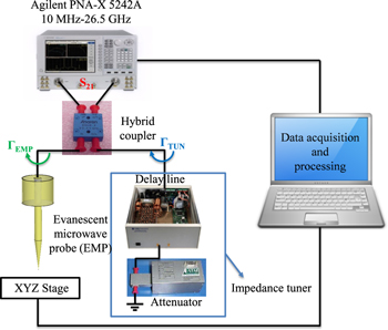
Figure 1. Interferometer-based near-field microwave microscope.
Download figure:
Standard image High-resolution imageAs illustrated in figure 1, the direct and coupled paths of the hybrid coupler are connected to the EMP (with reflection coefficient ΓEMP) and to the impedance tuner (with reflection coefficient ΓTUN) respectively. In this configuration, the coupler has two functions. First, it acts as a reflectometer that separates the incident signal from the one reflected by the EMP. Second, by combining the reflected signal by EMP with the wave coming from the impedance tuner, the interferometer gives the possibility to tune the measured signal to a very low level. Particularly, ΓTUN is carefully adjusted to compensate ΓEMP by varying the amplitude and the phase-shift of the impedance tuner made of a variable attenuator and a delay line. In these conditions, the measured transmission coefficient (zero-level signal) is given by [18]:

The signal resulting from the combination of ΓEMP and ΓTUN is measured in a transmission mode (S21) to reduce the directivity errors coming from the VNA, especially in the case of the measurement of low level signals.
In addition to the microwave part, the iNFMM also includes an x–y–z stage consisting of three independent motorized linear translation sub-stages with travelling distances of 25 cm on both the x and y axis and 1 cm on the z axis (figure 1). The minimum increment step in the three directions is 1 μm. The sample to be tested is placed on the chuck fixed on the stage whereas the microwave part of the microscope remains fixed. Consequently, better measurement stability is obtained by moving the sample under the probe tip instead of moving the probe. The probe (apex = 66 μm) is positioned vertically over the stage. A camera is used for better visualization of the tip and the sample under test. Concerning the software part of the platform, a National Instruments Labview interface is developed to control the position of the sample, to set the network analyzer parameters, to determine the resulting transmission coefficient S21 and to display the results.
3. Electromagnetic simulation of the probe–sample interaction
Simulation tools are available for a fine study of the electromagnetic properties of different kinds of structures. In this part, the electric filed distribution between the probe and the sample is investigated by using the electromagnetic simulation software 'AnsysTM/HFSS'.
In our case, the graphene flake is obtained by epitaxial method on silicon carbide. Thus, instead of employing the conductivity calculated by the Kubo equation [19], we use for the simulations the value obtained by DC measurement, 1 kΩ/square. Furthermore, the probe is simulated as a metallic conductor extruded out of a coaxial connector whose intrinsic impedance is designed to be 50 Ω. The tip of this probe is tapered to a semi-sphere shape with a diameter of 66 μm. Four samples have been considered for the simulation investigation: silicon carbide (SiC) used as substrate, epitaxial graphene (SiCG), gold-metallized SiC (MSiC) and epitaxial graphene with a Al2O3 layer prepared with static oxidation process on the top (SiCGAlO). For the demonstration, the electric field distribution of the probe at 2 GHz for the four samples is shown in figure 2. The probe is placed 10 μm over the sample surface, which guarantee a near-field and non-contact measurement.

Figure 2. (a) Configuration of the samples tested: silicon carbide (SiC) substrate, epitaxial graphene on SiC substrate (SiCG,) metallized SiC substrate with gold layer on the top (MSiC) and SiCG structure with Al2O3 layer on the top (SiCGAlO), (b) simulation of electric field at the cross-section along the probe, zoomed image of tip–sample (SiC) coupling and (c) electric field penetration in the samples (stand-off distance fixed at 10 μm), f0 = 2 GHz, simulation tool: AnsysTM/HFSS.
Download figure:
Standard image High-resolution imageAs shown in figure 2(b), the electric field is well confined around the probe apex. A discontinuity of the electric field is found at the air–sample interface due to the strong air–sample mismatch. Indeed, most of the electric field is reflected at the air–sample interface, and only a small part penetrates into the sample (SiC). The field penetration is illustrated for the four samples in figure 2(c). The penetration of electric field in these four samples is different from each other indicating a good measurement sensitivity. For the MSiC sample, there is practically no electric field distribution inside the SiC substrate as the electromagnetic field is shielded by the metal layer deposited on the top of SiC. Compared with the simple SiC substrate, the intensity of electric field in the SiCG structure is much smaller due to existence of conductive graphene layer, although the thickness of graphene layer is only 0.1 nm.
To better appreciate the electromagnetic coupling between the probe and the different samples, especially the electric field at the air–sample interface, the electric field distributions are plotted along a line from the tip end to the inside of the sample (figure 2(b)) for the four cases (SiC, MSiC, SiCG and SiCGAlO) in figure 3. As can be seen in figure 3(a), there is a field distribution discontinuity at the air–sample interface. For SiC, as shown in figures 3(a) and (b) (for a stand-off distance of 10 μm) the field falls from 1220 to 90 V mm−1 (reduction of a factor of about 13). Then, it is noticed that the addition of a layer on top of SiC reduces even more the strength of the field to attain very low values. To better visualize the behavior of the E-field in the sample, results for two additional stand-off distances (one lower 10 μm and another one larger) are given in figure 3(c) for SiC. As expected it is retrieved that the strength of the E-field in the sample is linked to the stand-off distance selected. Finally in figure 3(d), the effect of the stand-off distance on the MSiC sample is examined. We observed a small variation of the field in the sample even for a layer of gold on the top of SiC. That means that the field penetrated inside the metal layer and of course that the level depends on the stand-off distance also. All these results together confirm that the stand-off distance influences the strength of the E-field in the sample and that of course the distribution of the field depends on the sample under test.

Figure 3. Electric field distribution for the samples as a function of the distance from the tip end, f0 = 2 GHz: (a) distance from the tip end from 0 to 20 μm in case of a stand-off distance of 10 μm, (b) distance from the sample surface towards the inside of the sample in case of a stand-off distance of 10 μm, (c) distance from the SiC surface towards the inside of the sample in case of a stand-off distance of 5, 10 and 20 μm, and (d) distance from the MSiC surface towards the inside of the sample in case of a stand-off distance of 1, 5 and 10 μm.
Download figure:
Standard image High-resolution imageThe reflected microwave signal carries the samples' properties and gives actually the possibility to locally characterize the samples. This feature establishes the potential of the iNFMM to evaluate materials electromagnetic properties such as the surface impedance and the dielectric parameters. In the following the probe–sample interaction is studied on the basis of a lumped-element model and a calibration procedure of the platform is discussed.
4. Calibration procedure of iNFMM
4.1. Modeling of the probe–sample interaction
Understanding NFMM measurements requires some insights into the interaction between the probe and sample under test. As the sample is placed in the near-field range of the tip and given that the tip radius is much smaller than the wavelength, the probe–sample interaction can be represented by a lumped element network in the quasi-static approximation [20]. We present the schematic of this probe–sample interaction modelling in figure 4.
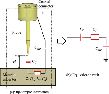
Figure 4. Schematic of a lumped element model of probe–sample interaction. Here, Cc is the coupling capacitance between the tip and the sample, Zs is the material impedance to be measured, including the resistance Rs, inductance Ls and Cs is the capacitance of the material. Cstr is the stray capacitance [2, 21].
Download figure:
Standard image High-resolution imageIn near-field region, the stray capacitance Cstr can be neglected because it is much larger than Cc [20]. Thus the lumped element model of such a probe–sample interaction can be simplified as a coupling capacitance Cc in series with the material impedance ZS. Particularly, in case of a metallized sample, in the first order of approximation, the interaction between the tip and the sample can be simplified and represented by a coupling capacitance Cc.
4.2. iNFMM calibration procedure
A calibration procedure is employed to transform the transmission coefficient S21 measured into the impedance of the device/material under test (ZS). The description of the calibration method and the material impedance extraction from the measured data (magnitude and phase-shift of the transmission coefficient) are illustrated in figure 5.
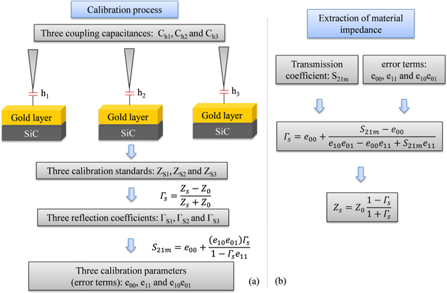
Figure 5. Calibration procedure of iNFMM (a) and the extraction of the material impedance (b).
Download figure:
Standard image High-resolution imageAs shown in figure 5, the calibration process is derived from a one-port VNA calibration method, requiring three standard impedances. The metalized SiC substrate is selected as the standard material for the calibration process and the probe sample interaction is modeled as said before by a coupling capacitance Cc. In general, there are basically two methods to analytically solve this capacitance: the image-charge method [21] and the surface integration method [22]. In this study, the image-charge method is used to determine the capacitance Cc. As the electromagnetic field is concentrated around the probe tip of semi-sphere shape and according to [23, 24] works, the capacitance CC between the semi-sphere and the metallic plane is given as follows:

where α = cosh−1(1 + a') with a' = h/R0. h is the stand-off distance between the tip and the sample. R0 is the tip radius. The impedance Zs of the sample can be related simply to the reflection coefficient Γs [25, 26] by:

where Z0 is the measurement system characteristic impedance (here 50 Ω: VNA impedance). When only the coupling capacitance Cc is considered, Zs can be written as:

 is the angular frequency. A traditional one port calibration model is used to link the transmission coefficient measured S21m to the reflection coefficient Γs (figure 5(a)).

The error terms, e00, e11 and e10e01, are respectively the directivity, matching and tracking errors. They can be determined by measuring three reflection coefficients for three known calibration standards ZS1, ZS2 and ZS3 with reflection coefficients ΓS1, ΓS2 and ΓS3. It should be mentioned that the calibration coefficients depend on the operating frequency. For example, if we consider for the calibration procedure, 10, 260, and 410 μm as the stand-off distance, we obtain based on the equation (2) 2.6 fF, 0.22 fF and 0.14 fF respectively for the corresponding coupling capacitance. One can note that the capacitance value decays rapidly with increasing stand-off distance. Then, relying on the equations (3)–(5), the calibration parameters retrieved at 2 GHz are e00 = 0.015/−81.1°, e11 = 3.9 × 10⁻⁶/−178.7° and e01e10 = 0.99/−0.024°. Once these three calibration parameters are determined, the electrical properties are extracted from the transmission coefficient according to the flow-chart given in figure 5(b). This calibration process is repeated for each frequency point considered.
5. Results and discussions
5.1. Evaluation of the measurement sensitivity
The quality factor of the iNFMM represents one of the most effective parameters to demonstrate the measurement sensitivity [1, 27]. As reported in the literature, the transmission-line-based structures usually exhibit a quality factor in the order of 1000 [3, 28, 29]; while the resonator-based platforms present higher Q values around 5000 [5, 30]. Unfortunately, all these platforms are narrow band and thus enable high measurement sensitivity in a limited frequency band. In contrast, an interferometer-based structure has the potential to achieve a good sensitivity in a broad frequency band. For example, Bakli et al obtained a Q varying from 5300 to 9400 in the frequency band (2–6 GHz) in free space [31] considering a zero level of −60 dB (30 dB above the noise floor of −90 dB of the VNA for an IFBW of 100 Hz). In this work, we extend the working frequency range up to 18 GHz with an excellent sensitivity (Q in the order of 53 000). The zero level is set around −75 dB (15 dB above the VNA noise floor) by carefully tuning the attenuator and the delay line when the probe is placed in air. The intermediate frequency bandwidth (IFBW) and power of the VNA (P0) are set to 100 Hz and 0 dBm, respectively.
Generally, λ/4 or λ/2 coaxial resonator based NFMMs are used to retrieve the materials/devices under test properties from the measurement of the quality factor and resonant frequency [1]. Nevertheless, since recently, the TLM is exploited more and more in AFM-based NFMM [25, 32]. The proposed iNFMM has the advantage of being operable with both resonator and TLMs. First, the measured quality factor (Q) and the resonance frequency shift (Δf) as a function of the probe–sample distance are shown in figure 6. In fact, Δf represents the difference between the resonance frequency obtained when measuring the sample under test (fmeas) and the reference resonance frequency (fref) measured without sample under test. In this study, the reference frequency selected is 2 GHz. The stand-off distance selected goes from 10 μm, to guarantee the tip–sample interaction is in the near field, to 510 μm (h ≫ apex size). In NFMM systems the distance control between the probe and the sample is a key parameter. The resolution and therefore the precision on the quantities measured is directly related to the accuracy with which the distance probe–sample is controlled. Different techniques can be used to ensure a fine control of the distance. For example, for experiments in the nanometer scale generally the probe-tip is mounted onto a quartz tuning-fork oscillator [33]. In our case, for distances in the micrometer range, the tip–sample distance is determined by the following process. First, the probe tip approaches the sample surface gently, and once the tip touches the surface, the contact position is noted as 0. Then, this reference position is used to set the displacement of the tip by using the stage.

Figure 6. Measured quality factor (a) and resonance frequency shift (b) of transmission coefficient ∣S21∣ as a function of the stand-off distance; f0 = 2 GHz, IFBW = 100 Hz, P0 = 0 dBm, the wave-cancelling process is done considering the probe in air with zero level = −75 dB.
Download figure:
Standard image High-resolution imageThe four samples have different microwave responses in terms of quality factors and resonance frequency shifts qualifying the method for material quality analysis. It is observed in figure 6(a) that the quality factor increases when increasing the tip–sample distance h. This is due to the fact that the quality factor (QRef) is tuned to the max (53 000) for the reference measurement (no sample under test). The total quality factor (Qt) is given by  where Qin is the intrinsic quality factor of the material under test and Qc is the coupling quality factor dominated by the capacitance between tip and materials. Thus, the quality factor variations Qt measured at the same height indicate the different internal losses including dielectric losses for these four samples. Values of Qin are proportional to dielectric losses tanδ [34]. By extracting impedance from measured S21 of both SiC and SiCGAlO samples, we obtain values of tanδ(SiCGAlO) = 0.3456 which is much higher than tanδ(SiC) = 9.2 × 10⁻⁵. It corresponds to the results given in figure 6(a) showing that the SiCGAlO quality factor is much lower than that of SiC. Due to the conductivity of graphene and gold, most of the electromagnetic field is reflected, SiC substrates are thus shielded. In other words, dielectric losses from SiC in SiCG and MSiC contribute less efficiently in reducing the total quality factor in this measurement in which Q exhibits similar values in both two samples. It is easy to understand the frequency shift phenomenon when we treat samples as RLC circuit in series. Both SiC and SiCGAlO samples add big capacitance in series in the circuits which makes resonance shift. However, again, the resonance shift difference between SiCG and MSiC are quite close. Compared with the simple metal layer, the graphene layer contributes not only to the inductance but also to the capacitance [35]. The measured imaginary part of graphene impedance (see figure 9) is positive which indicates the contribution of this capacitance effect may be quite small. A further mesoscopic model is required to give precise explanation for the frequency shift difference between SiCG and MSiC. But the clear difference between SiC and SiCG in quality factor and resonance shift measurement demonstrates that this iNFMM technique provides a new method to verify for example the uniformity of graphene grown on SiC substrate instead of using AFM.
If we look now at the second treatment method of the data we can plot the magnitude and phase-shift of the transmission coefficient S21 (figure 7).
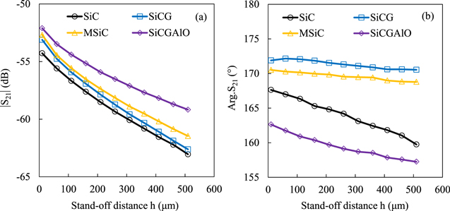
Figure 7. Measured magnitude (a) and phase-shift (b) of the transmission coefficient S21 as a function of the stand-off distance; F0 = 2 GHz, IFBW = 100 Hz, P0 = 0 dBm, the wave-cancelling process is done considering the probe in air with zero level = −75 dB.
Download figure:
Standard image High-resolution imageAs shown in both the magnitude and phase-shift plots the four samples can be easily distinguished by the proposed iNFMM. One can also note that as the zero level selected (−75 dB) is adjusted when the probe is in air, the ∣S21∣ decays as a function of the stand-off distance. The phase-shift spectra of S21 are also affected by the distance separation between the probe and the materials but in proportions depending on the material under test. Thus, this technique demonstrates its potential for the investigation of the local electromagnetic properties of samples with high sensitivity.
Now, for the demonstration, based on the magnitude and phase-shift of the transmission coefficient, we present the results of the implementation of the calibration process described before to extract the electric properties of the material under test.
5.2. Extraction of the impedance of materials under test
When the iNFMM operates in the non-contact mode, the measurement accuracy can be influenced by the separation between the probe and the sample under test. Thus, the extracted electric properties are evaluated as a function of the stand-distance. For the demonstration, the substrate (SiC) is selected as the sample under test. Thanks to the calibration process detailed before, the measured transmission coefficient S21 is translated to the impedance of the sample under test. The probe–SiC interaction is simply modeled as a coupling capacitance (ZC) in series with the impedance of SiC (ZSiC), and thus ZSiC can be extracted by subtracting ZC from the total impedance ZS1 (ZS1 = ZC + ZSiC). Then, from the knowledge of ZSiC the dielectric properties of SiC can be determined. In figure 8, the extracted ε' and tanδ of SiC versus the stand-off distance and also versus the frequency are presented.
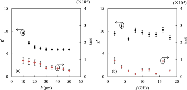
Figure 8. Extracted dielectric parameters of SiC after the calibration procedure: (a) ε' and tanδ as a function of the stand-off distance h at 2 GHz, (b) ε' and tanδ as a function of the frequency when the distance is kept to 10 μm.
Download figure:
Standard image High-resolution imageIn figure 8(a), the dielectric constant obtained at a small distance, ε' (h = 10 μm) = 9.6, agrees well with the value found in the literature [36]. It is observed that this value diminishes with the stand-off distance between 10 and 30 μm and then is almost constant around 6. Indeed, with the increasing stand-off distance, the electromagnetic coupling between the probe and the sample is weakened, resulting in a reduced wave penetration into the SiC substrate and a larger influence of the air gap between the sample and the tip. Thus, to guarantee a good performance of the platform, the stand-off distance is kept as small as 10 μm for the following. Additionally, the losses level retrieved in figure 8(a) (below 10−4) also agree well with the literature data. Then, the broadband behavior of the dielectric parameters from 2 to 18 GHz is shown in figure 8(b). The extracted dielectric parameters are also comparable to the theoretical values found in the literature [37].
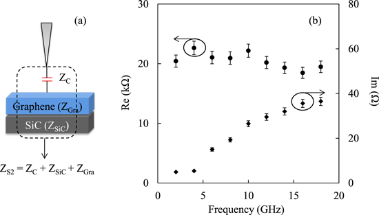
Thanks to the knowledge of the SiC properties, the impedance of the graphene flake (ZGra) can be solved in a similar manner. As modeled in figure 9(a), ZGra can be extracted from ZS2 which consists of three impedances in series: ZC, ZGra and ZSiC. The real and imaginary parts of impedance retrieved for graphene are presented in figure 9(b).
Figure 9. Modeling of the probe-SiCG interaction (a) and extracted complex impedance of graphene (b) as a function of frequency from 2 to 18 GHz.
Download figure:
Standard image High-resolution image
As shown in figure 9, the surface resistance of graphene is in the order of 20 kΩ from 2 to 18 GHz. When comparing the resistance obtained with the value measured by other approaches, we note that this resistance extracted by iNFMM is higher than the values retrieved by dc probing and CPW methods, but corresponds to the values acquired by the NFMM method ranging from tens to hundreds of kΩ [6, 14, 37]. Actually, as a 2D material with a thickness in atomic scale, the graphene flake presents a dielectric behavior with low conductivity in the vertical direction [38, 39]. This can explain the high surface resistance measured by iNFMM, in the order of 20 kΩ, as the microwave beam sent out by the probe illuminates vertically the sample (figure 9(a)). On the other hand, the imaginary part of the graphene impedance is also given in figure 9. The reactance of graphene is practically proportional to the frequency varying from 4.9 Ω at 2 GHz to 36.5 Ω at 18 GHz, which corresponds to an average inductance of about 360 pH. It is worth noting that these extracted values represent the local surface impedance of the graphene. Furthermore, the impedance measured represents the value of an area corresponding to the tip projection onto the graphene surface. Considering the tip end as a semi-sphere shape (D = 66 μm), the projected area on the graphene surface is about 3420 μm2. This capability of local characterization offers possibility to detect inhomogeneity from the mapping of materials.
6. Conclusion
In this paper, a broadband non-destructive and non-contact characterization of epitaxial graphene is realized by using an iNFMM. Thanks to the interferometric technique, high measurement sensitivity can be obtained at any desired operating frequency from 2 to 18 GHz. The probe–sample interaction is theoretically studied by using the electromagnetic simulation software, AnsysTM/HFSS. Simulation results demonstrate a strong electromagnetic coupling between the probe tip and the sample, allowing a very local evaluation. The measurement sensitivity is experimentally validated by measuring both the quality factor and shift of resonance frequency of different samples including silicon carbide (SiC) used as a substrate, epitaxial graphene (SiCG), gold-metallized SiC (MSiC) and epitaxial graphene with Al2O3 layer on the top (SiCGAlO). Finally, a calibration method is proposed to extract the complex impedance of a graphene flake grown on a silicon carbide substrate. Materials with known electrical properties are regarded as the calibration standards. The graphene flake is characterized as a resistance (∼20 kΩ) and a small inductance (360 pH). The retrieved resistance is comparable with the values obtained by platforms such as AFM-based NFMM. The advantage of the proposed method is its non-contact and non-destructive features; there is no need to fabricate electrodes on the sample surface for the characterization. This work actually contributes to a preliminary study for the local characterization of 2D materials.