

Abstract
Titanium oxide/silicon oxide (TiO2/SiO2) 2D patterns were obtained by magnetron sputtering depositions of Ti on close-packed and size-reduced colloidal masks on Si and quartz substrates, followed by mask lift-off and ending with thermal oxidation. The physical processes involved in growing 2D Ti patterns and their oxidation are analyzed. For the magnetron sputtering deposition, two regimes are considered: the low-pressure regime when the flux of sputtered atoms is anisotropic, and the high-pressure regime, when the flux of sputtered atoms is isotropic due to frequent collisions. Moreover, magnetron sputtering operation modes, such as dc sputtering and high power impulse sputtering, are compared. The changes in pattern size and morphology determined by the oxidation of the Ti patterns and Si substrate are analyzed. The hydrophilicity induced by UV-light irradiation and the visible-light photocatalytic activity towards the degradation of the methylene blue of the fabricated TiO2/SiO2 patterns were considerably higher when compared to the performances of uniform TiO2 films.
Export citation and abstract BibTeX RIS
1. Introduction
The discovery of the ability of spherical nanoparticles from a colloidal solution to self assemble on substrate surfaces [1] opened up the opportunity for the construction of nano masks to be used in etching or depositions for the fabrication of 2D nanopatterned surfaces with a relatively large, but limited, choice of motives and shapes. The whole nanofabrication process has been called nanosphere lithography (NSL) [2] and is nowadays intensely investigated for the fabrication of 2D nanopatterned surfaces with applications in cell biology [3], biosensors [4, 5], photonic crystals [6, 7], optoelectronic devices [8], and surface wetting [9]. Various materials (metals, oxides, polymers, self assembled molecular layers, etc) can be nanopatterned by this technique on a wafer-scale area with relatively low-cost and high throughput. The motives and shapes of the resulting 2D patterns depend very much on the choice of masks and deposition/etching techniques. Masks consisting of a single layer or a bilayer of close-packed nanoparticles [10], a layer of sparse charged nanoparticles [11], or a layer of particles with two distinct sizes [12], etc, have been used to produce various 2D nanopatterns by physical vapour depositions. Moreover, these masks can be modified by annealing [13] and/or reactive ion etching (RIE) [14] to obtain more control on the resulting 2D patterns. On the other hand, control of the shape and motives of the 2D nanopatterns obtained by physical vapour deposition can be achieved by modification, during depositions, of the orientation of the substrates with colloid masks with respect to the vapour source, a technique called angle-resolved NSL [15].
Among various etching and deposition techniques, plasma deposition and etching are very successful in the fabrication of nanostructured surfaces [16]. In the present paper we analyze the characteristics of titanium (Ti) 2D patterns obtained by magnetron sputtering depositions on closely-packed and size-reduced colloidal masks (CPCM and SRCM, respectively). The SRCMs are obtained by RIE of the CPCMs. Two sputtering deposition techniques are analyzed—dc magnetron sputtering (DCMS) and high power impulse magnetron sputtering (HiPIMS). While the DCMS operates at a constant low discharge power (density of power at the target surface from a few W cm−2 to a few tens of W cm−2), the HiPIMS is a pulsed discharge that operates with very short (from a few microseconds to a few hundred microseconds) and powerful (power density at the target surface of a few KW cm−2) discharge pulses applied to the cathode with a repetition frequency around 1 kHz. While the DCMS is a physical vapour deposition (PVD) technique producing vapour by sputtering, the HiPIMS deposition is an ionized PVD technique because a large fraction of the sputtered material is ionized [17]. Due to ionization and the higher energy of the sputtered atoms, the HiPIMS depositions produce much denser films as compared to DCMS depositions. The pressure of the working gas (usually argon (Ar)) used in magnetron sputtering deposition also has a tremendous effect on the compactness and morphology of the deposited films. It is well known that magnetron sputtering in gaseous plasma works in a limited range of gas pressure values [18]. At a higher limit of the working pressure range (high-pressure working regime), the sputtered atoms are scattered by elastic and inelastic collisions, thus having lower energies and a wider distribution of incidence angle values on the growing film (isotropic deposition). On the other hand, at a lower limit of the working pressure range (low-pressure working regime), the sputtered atoms are more energetic and reach the growing film with the background gas atoms suffering collisions (anisotropic deposition). Molecular dynamic simulation studies of the film growth have shown that energy and incidence angle distribution of sputtered atoms have a tremendous impact on the structure of the growing films [19]. Depositions of films with a rough columnar structure are favored by the low energy and wide incidence angle distribution of sputtered atoms in the high pressure regime, while depositions of smooth, compact and conforming (to the substrate topography) films are favored by the high energy and narrow incidence angle distribution of the sputtered atoms in the low-pressure regime. Therefore, a significant effect of the working gas pressure on the structure and morphology of both deposited films and 2D patterns is expected. In the present work, the low- and high-pressure working regimes are considered to be in agreement with the results of the Monte Carlo simulation and laser-induced fluorescence measurements of the velocity distribution functions of sputtered Ti atoms in a DCMS system [20]. These results indicated an isotropic velocity distribution for the sputtered Ti atoms in DCMS working at a high pressure of Ar gas (30 mTorr) and an anisotropic velocity distribution for the sputtered Ti atoms in DCMS working at a low pressure of Ar gas (3 mTorr). Therefore, we provide a detailed comparison of the 2D patterns obtained by the two deposition techniques working in regimes of high- and low-pressure. Finally, the silicon (Si) substrates with the deposited Ti 2D nanopatterns are oxidised by annealing in a pure oxygen atmosphere to obtain titanium oxide/silicon oxide (TiO2/SiO2) 2D nanopatterned surfaces with enhanced photocatalytic activity in visible light. Kannaiyan et al [21] have shown that TiO2/SiO2 patterned surfaces have a better visible-light photocatalytic activity towards decomposition of methylene blue (MB) in aqueous solution than the nano-dot covered TiO2 surfaces. The enhanced photocatalytic activity of a TiO2/SiO2 patterned surface has been attributed to a good adsorption of dye molecules on the SiO2 surface along with their diffusion to the TiO2 surface, where they are subjected to redox reactions. The TiO2 nanostructured surfaces can be coupled with metal co-catalysts to enhance the photocatalytic activity. Zhang et al [22] coupled the TiO2 porous surface (nanotube arrays) with gold nanoparticles to enhance the visible-light photocatalytic activity of TiO2 by coupling the plasmon light absorption in gold nanoparticles with the generation of charge carriers in TiO2. In this work, we investigate the visible-light photocatalytic activity of the fabricated TiO2/SiO2 2D patterns towards the decomposition of organic molecules (MB) in aqueous solutions under visible light irradiation. The wetting property of the fabricated 2D nanopatterned surfaces is also investigated.
2. Experiment
2.1. Materials
Aqueous solutions of polystyrene (PS) nanospheres with a diameter of 500 nm (10 wt%), ethanol (99.8%), acetone (99.8%) and MB (99.8%) were purchased from Sigma Aldrich. Deionized water (electric resistivity > 18 MΩ · cm) was prepared by a Milli-Q filtering system (Super-Q® Plus System from Merk Millipore). The targets used in the depositions (99.995% purity Ti disks with 5 cm in diameter) were purchased from Kurt J Lesker.
2.2. Fabrication of 2D Ti and TiO2 patterns
TiO2 nanopatterns were obtained by magnetron sputtering of Ti on quartz and Si substrates with CPCMs and SRCMs, followed by lift-off of the masks with the deposited films, and thermal oxidation by annealing the 2D patterns in a pure oxygen atmosphere at 900 °C. The main processing steps used in the fabrication of the patterns are presented schematically in figure 1.
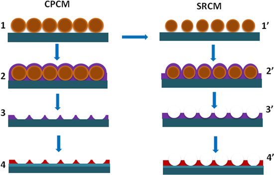
Figure 1. Schematic of the processing steps used in the fabrication of TiO2/SO2 patterned surfaces: (1) deposition of CPCMs by spin coating; (1') reactive ion etching in oxygen plasma of CPCMs to obtain SRCMs; (2) and (2') deposition of Ti thin films by DCMS and HiPIMS; (3) and (3') lift-off of colloidal masks with the deposited films by sonication; (4) and (4') thermal oxidation of Ti/Si 2D patterns to obtain TiO2/SiO2 2D patterns.
Download figure:
Standard image High-resolution imageBefore the mask depositions, the Si and quartz substrates (1.5 × 1.5 cm2) were cleaned in an ultrasonic bath (10 min in acetone, 20 min in ethanol, followed by rinsing with DI water and drying in nitrogen flow). Then, the substrates were further cleaned and hydroxylated by exposure to low-pressure plasma of water vapour and air mixture for 10 min [23]. This step considerably improved the quality of the CPCMs deposited by spin coating because the plasma treatment enhanced the substrate wetting property and promoted the formation of hydrogen bonds between the PS nanospheres and the substrate surfaces [24]. The as-received PS colloidal solution was diluted with deionized water to a concentration of 0.8 wt.% and subsequently mixed with ethanol in a 1:1 ratio. The mixture was sonicated for 10 min to disperse the PS nanospheres. A small amount of the diluted colloidal solution (90 μl) was deposited and spread instantaneously on the substrate, which was then loaded on the spin coater machine (Laurell Technologies WS-650).
The spin-coating process was performed in four consecutive steps: (a) 200 rpm for 30 s and (b) 400 rpm for 1 min to spread the PS bead solution evenly; (c) 800 rpm for 2 min to spin away the excess PS bead solution; (d) 4000 rpm for 20 s to spin away the excess materials from the edges. The spin coating deposition resulted in depositions of CPCMs consisting of a monolayer of hexagonally close-packed PS beads that were used in magnetron sputtering depositions for the fabrication of Ti nanopatterns. Some CPCMs were subjected to RIE to obtain SRCMs. The RIE used plasma of a radio frequency discharge (power of 50 W) in oxygen gas (purity of 99.999%) at a flow rate of 10 sccm and a pressure of 50 Pa. The flow rate of O2 gas was controlled by a mass flow controller (MKS), while the pressure was monitored with a full range pressure gauge (Agilent Technologies). The substrates with CPCMs were loaded on the cathode (stainless steel disk with 8 cm in diameter) of the radio frequency discharge chamber. Before etching, the base pressure in the chamber was maintained for 2 h at approximately 1 × 10⁻⁶ Torr by a dry (oil free) vacuum pumping system. The self-bias potential of the cathode surface during the discharge was around −300 V. The size and shape of the etched nanospheres was controlled by adjusting the etching duration and gas pressure and maintaining the RF power constant. The relatively large value of the gas pressure used in our RIE experiments determined isotropic etching at relatively small etching rates, which allowed for a good control of the shape and size of the etched masks. The RIE time was fixed to 1 min to obtain a reduction of the PS bead diameter from 500 nm to about 400 nm. Analysis of the shape and size of the etched PS beads was performed by atomic force microscopy (AFM). AFM images of a CPCM and a SRCM obtained by RIE are given in the supporting information (SI) (figure SI1 is available online at stacks.iop.org/NANO/28/255302/mmedia).
The Ti thin films were deposited on Si and quartz substrates with the colloidal masks of PS beads using DCMS and HiPIMS techniques. Before deposition, the base pressure of the deposition chamber was maintained for 2 h at approximately 1 × 10⁻⁷ Torr by a dry (oil free) vacuum pumping system. During the depositions, the flow rate of Ar (purity of 99.999%) was kept constant at 10 sccm by a mass flow controller (MKS), while the pressure was monitored with a full range pressure gauge (Agilent Technologies). The operating pressure (3 or 30 mTorr, respectively) was controlled by the opening of a gate valve connecting the vacuum pumping system to the deposition chamber. All the deposition runs were carried out by sputtering a pure Ti (99.995%) disk (magnetron target) with a diameter of 2 inch in Ar gas at a constant average power (100 W) and a target-substrate distance (100 mm). For the DCMS operation, a dc power supply (PNC 400–1500 from Heinzinger) was connected to the magnetron and set to deliver a constant average power of 100 W at a voltage applied to the cathode versus the grounded deposition chamber of about −300 V. For the HiPIMS operation, the magnetron was powered by a homemade high power pulse generator with the pre-ionization voltage set to maintain a constant discharge current intensity of about 8 mA between pulses. Ultra-short voltage pulses (5 μs duration) with an amplitude of −1 kV were applied to the magnetron cathode to determine high power discharge pulses with peak values of the current intensity in the range 30–40 A. The HiPIMS pulse repetition frequency was varied to obtain an average value of the discharge power of 100 W in both high- and low-pressure regimes. More details on our HiPIMS system used for the depositions of Ti and TiO2 thin films are given elsewhere [25]. The deposition time, the operating mode and the operating pressure were selected as variable parameters in order to produce depositions of films with the same superficial density of mass, parameter that was monitored by a quartz crystal microbalance (Q-pod Infincon) placed beside the substrate holder and facing the target. After the depositions, the colloidal masks with the deposited films on top were removed by sonication in DI water for 3 min. This operation left the 2D nanopatterns of Ti on the Si or quartz substrates. Finally, using a programmable substrate heater from Neocera, the Ti/Si 2D patterns were thermally oxidised in oxygen atmosphere at 900 °C for 2 h to obtain the TiO2/SiO2 2D patterns. The oxidation was performed in the same chamber (also used in the depositions) vacuumed at 1 × 10⁻⁷ Torr and filled with pure oxygen (purity of 99.999%) at the atmospheric pressure.
2.3. Measurements
The cross-sectional scanning electron microscopy (SEM) images of the CPCM of the PS beads with Ti coatings were obtained by using a Carl Zeiss Crossbeam Neon 40ESB FIB/SEM microscope. The AFM investigations were performed in air with a commercial AFM apparatus (XE 70 from Park, South Korea) working in non-contact mode with a Si AFM probe (MikroMasch HQ:NSC35/NoAl) with a sharpened tip (nominal curvature radius of 8 nm) and a stiff cantilever (nominal resonant frequency and force constant of 150 kHz and 5.4 N m−1, respectively). The topography AFM images were levelled to the planar surface of the substrate (height = 0) by homemade Matlab processing and analyzing software. The height profiles of the patterns were extracted from the AFM topography images and processed to remove the AFM tip-sample convolution effects by the inverse tip image method [26]. The crystalline structure of the Ti thin films deposited on CPCMs and TiO2 patterns obtained with SRCMs were studied by an -ray diffractometer (PANalytical X'pert PRO MPD) using Cu Kα radiation (λ = 0.15418 nm) in the Bragg–Brentano configuration. The UV–vis absorption spectra of the Ti and TiO2 2D patterned surfaces were obtained by a UV–vis spectrophotometer (Evolution 300 from Thermo Scientific). The photo-induced hydrophilicity was evaluated by measurements of the water contact angle for TiO2/SiO2 2D patterned surfaces irradiated by UV light. The water contact angle measurements were performed at room temperature by analysis of the profile images of small sessile water droplets captured by a digital microscope. The probes were radiated by a UV lamp (TUV T8 from Philips) at a power density of 1.8 mW cm−2.
The photocatalytic activity of the TiO2/SiO2 2D patterns was characterized by measuring the degradation rate of MB dye in aqueous solutions under visible light irradiation. The concentration of MB in solution was determined by measurements of optical absorbance in the 400–800 nm range (with a peak in the absorption at 664 nm) by a UV–vis spectrophotometer (Evolution 300 from Thermo Scientific). The UV–vis spectrophotometer was first calibrated in order to determine the relationship between the absorbance peak intensity and MB concentration. Then, a solution with an initial concentration of 440 ppm MB was prepared and used in the photocatalytic degradation experiments. The TiO2/SiO2 2D patterned probes were incubated in a 5 ml solution of MB, left in the dark for 5 min and then irradiated with visible light (λ > 400 nm) at a constant power density of 60 mW cm−2.
3. Results and discussion
3.1. Magnetron sputtering deposition of Ti thin film on substrates with closely-packed colloidal masks
Ti thin films with the same mass per area unit were deposited by DCMS and HiPIMS techniques on Si substrates with CPCMs of PS beads 500 nm in diameter. The SEM (figure 2) and AFM (not shown) images of the deposited Ti films show a strong effect of working gas pressure on the density, morphology and surface topography of the deposited films. At a high pressure (30 mTorr) the CPCM acts as a template for the columnar growth of low density polycrystalline films. The low density of these films is indicated by their thickness, a larger film thickness at the same mass per area unit indicating a lower density. Moreover, depositions in the high-pressure regime on substrates tilted at 45° with respect to the magnetron target showed that the columns always grow perpendicular to the substrate (see figure SI2 of the SI). This occurs because at large working gas pressure values the deposition is isotropic, which enhances the shadow effects of the mask with the growing film, i.e. the Ti atoms moving with large incidence angle values are shadowed by the highest local topography features and are, therefore, deposited preponderantly on the lateral sides of the highest features. Due to this effect, the top surface of the deposited film loses the spherical shape of the colloidal mask beads. This is shown in figure 3 by the film height profile along a line of beads. The height profile was obtained by analysis of the AFM topography images of the deposited films. The height profile shows, in agreement with the SEM images, that the top of the columns grown on the PS beads have a conical rather than a spherical shape. Also, small topography features that may be associated with the polycrystalline structure of the film are clearly visible in both the SEM and AFM images. At the low pressure (3 mTorr), the depositions are more anisotropic and more conform to the topography of the colloidal masks. The deposited films were much denser (smaller thickness) due to the higher mobility of the adatoms, which in this case are more energetic due to a much smaller collision frequency. The SEM images indicate the deposition of the films with smooth surfaces with the surface topography conforming with the CPCMs underneath. The height profile of the surface of the film deposited by DCMS at low pressure along a line of beads (figure 3) shows, in agreement with the SEM image, that the film surface maintains, with a certain increase of the curvature radius, the spherical shape of the beads underneath. Anisotropic deposition of Ti films by magnetron sputtering at low working gas pressure values is confirmed by SEM images of the films deposited on substrates tilted at an angle of 45° with respect to the sputtered target (see figure SI2 of the SI). In this case, preponderant film deposition along the direction of the sputtering target is clearly visible.
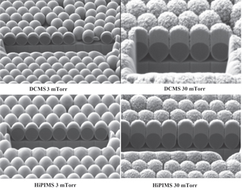
Figure 2. SEM images of Ti films deposited on colloidal masks by DCMS and HiPIMS at two working gas (Ar) pressure values, 3 mTorr and 30 mTorr. The images show cross sections of rectangular holes milled by FIB. The magnification of SEM images is not the same. The length scale on each image is indicated by the diameter of the PS beads, which is 500 nm.
Download figure:
Standard image High-resolution image
Figure 3. Height profiles of Ti films deposited on CPCMs by DCMS at two working gas pressure values (3 and 30 mTorr).
Download figure:
Standard image High-resolution imageThe characteristics of the Ti 2D patterns remaining on the Si substrate, after the CPCMs with deposited films were lifted off, were also dependent on the pressure of the working gas and the deposition technique. Figure 4 shows the AFM images of the patterns obtained by the two deposition techniques at low (3 mTorr) and high (30 mTorr) working gas pressure values. The corresponding SEM images of these patterns are shown in figure SI3 of the SI. Well-defined patterns that were larger in height were obtained on depositions at a low working gas pressure (3 mTorr). This occurred because, in the anisotropic depositions, more metal atoms can pass through the opening spaces of the CPCMs and thus contribute to the growing of the pattern. However, the opening spaces of the CPCM shrink during the film growth and, at a certain moment, the pattern ceased to grow because the deposition completely filled the mask openings. Therefore, there is a maximum height of the deposited patterns, which depends on how fast the openings of the colloidal masks are filled by the growing film. For the depositions at the high working gas pressure (30 mTorr), the growth of the film on the lateral features of the colloidal mask is enhanced due to the isotropy of the deposition, and the mask openings are filled much faster. This and the isotropy of the flux of metal particles reaching the growing pattern contribute to depositions of less well-defined 2D patterns, smaller in height, at this working gas pressure. Analysis of the pattern height profiles (see figure 5) along a symmetry direction of the pattern (segment AB shown in figure 4) illustrates these findings. Because the opening spaces of the CPCM are filled more slowly, the maximum height of the 2D pattern obtained by film depositions at low pressure is much larger. Also, at low working gas pressure values, the deposition technique has a greater impact on the fabricated 2D patterns. The HiPIMS deposition at a low working gas pressure produced the most well defined Ti pattern. This occurs because, in HiPIMS, a large fraction of sputtered atoms is ionised, and the ions are attracted to the negatively charged surface of the growing film. Also, the sputtered atoms are more energetic in HiPIMS than in DCMS.
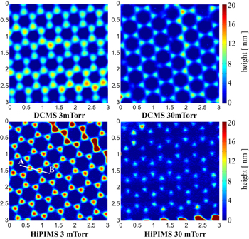
Figure 4. AFM images (3 μm × 3 μm) of 2D Ti nanopatterns obtained by DCMS and HiPIMS depositions at two working gas (Ar) pressure values, 3 mTorr and 30 mTorr.
Download figure:
Standard image High-resolution image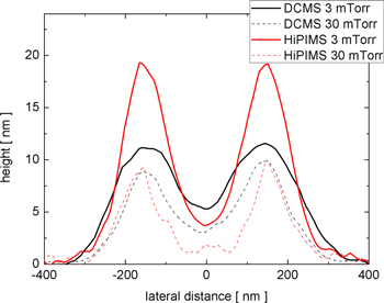
Figure 5. Height profiles of Ti 2D patterns grown on Si substrates with colloidal masks by DCMS and HiPIMS depositions at two working gas pressure values.
Download figure:
Standard image High-resolution image3.2. Magnetron sputtering deposition of Ti thin film on substrates with size-reduced colloidal masks
Depositions with CPCMs resulted in the fabrication of 2D patterns that were small in height due to the smallness of the opening spaces left by the masks for pattern deposition. We noticed that the patterns were much higher at CPCM defects that allow larger opening spaces. An AFM image illustrating an increase of pattern height along a defect line of a CPCM is provided in figure SI4 of the SI. Therefore, a well-defined 2D pattern with a larger height can be obtained if opening spaces left by the colloidal mask are enlarged by reducing the size of the beads of the CPCMs. Therefore, Ti thin films with the same mass per area unit were deposited by DCMS and HiPIMS techniques on Si and quartz substrates with size-reduced colloidal masks (SRCMs) of PS beads. The SRCMs were obtained by RIE of the CPCM to reduce the PS bead diameter from 500 nm to about 400 nm. Figure 6 shows the AFM images of the 2D patterns of Ti on Si substrates obtained with SRCMs by the two deposition techniques working at low (3 mTorr) and high (30 mTorr) gas pressure values. The patterns look like relatively uniform Ti thin films with a lattice of holes that retains the hexagonal symmetry of the CPCM. The height of the patterns is about 50 nm, except the pattern obtained by HiPIMS working at low pressure (3 mTorr), which has a height of about 35 nm. This is clearly indicated by the height profiles of the patterns (figure 7) along a symmetry direction of the pattern (segment AB in figure 6).
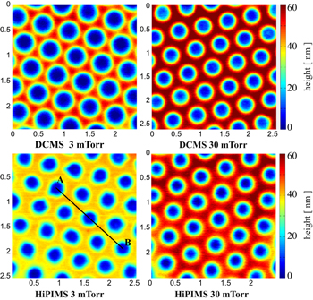
Figure 6. AFM topography images (2.5 μm × 2.5 μm) of Ti patterns obtained with SRCMs by DCMS and HiPIMS depositions at two working gas pressure values (3 and 30 mTorr). The height colour scale is the same for all images (0–60 nm).
Download figure:
Standard image High-resolution image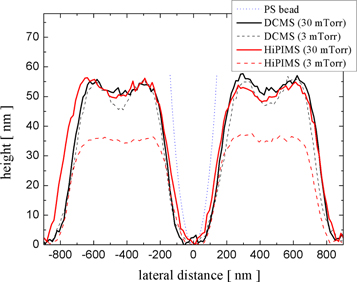
Figure 7. Height profiles of Ti patterns obtained by DCMS and HiPIMS depositions with SRCMs at two working gas pressure values (3 and 30 mTorr). A profile of a PS bead of SRCM with a diameter of 400 nm is shown on the central hole of the pattern.
Download figure:
Standard image High-resolution imageFor all patterns, the height profiles indicate that the holes are much larger than the PS beads of the SRCM (around 400 nm in diameter). This is explained by the shadowing effects of the SRCMs in totally or partially isotropic depositions. According to the SEM and AFM images (not shown) of the film grown on the SRCMs, the film also deposited on the lateral sides of the beads, thus reducing the open spaces of the SRCMs. Therefore, this narrowing of the mask open spaces during depositions determined patterns with enlarged holes (compared to the beads of the mask).
The Ti thin films deposited on the colloidal masks have polycrystalline structures irrespective of the deposition technique and working gas pressure value. Figure 8 shows the x-ray diffraction (XRD) patterns of the Ti thin films deposited on CPCMs by DCMS and HiPIMS techniques working at low and high gas pressure values. The broadening and shape of the diffraction peaks can be attributed to the smallness of crystallites and to the internal strain of the deposited films. Scherrer's equation [27] determines the values to be between 5 and 20 nm for the size of nanocrystallites in the film structure. The size of the nanocrystallites increased slightly with an increase in the working gas pressure used in both deposition techniques. The HiPIMS deposition technique tends to produce films with slightly larger nanocrystallites as compared to the DCMS deposition technique. Unfortunately, we could not obtain diffraction patterns for the Ti 2D nanopatterns left on the substrate after the lift-off because of the small amount of Ti on the Si substrates.
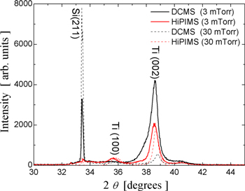
Figure 8. XRD pattern of Ti films deposited on CPCMs by DCMS and HiPIMS at two working gas pressure values.
Download figure:
Standard image High-resolution image3.3. Thermal oxidation of 2D Ti patterns
The 2D Ti patterns on the Si substrates were oxidised by annealing at 900 °C in pure oxygen gas at the atmospheric pressure for 2 h. The surface topography of the resulting patterns was analyzed by AFM. As a result of oxidation, the height and volume of the patterns increased.
Figure 9 shows the comparative Ti patterns obtained by DCMS depositions at low- and high-pressure working gas values (left side) and the TiO2 patterns resulting from their oxidation (right side). For a more quantitative comparison, the height profiles of the patterns along the segment AB in figure 9 are shown in figure 10. The height profiles indicate that the oxidation determined an increase of the profile height by a factor of 2.7 for the Ti patterns deposited at a high working gas pressure and of 1.6 for the Ti patterns deposited at a low working gas pressure. Interestingly, the increase of the pattern volume is noticeable only on the direction perpendicular to the substrate, the lateral dimensions of the patterns being roughly the same. The increase of volume by the oxidation of Ti can be estimated by considering the conservation of the number of Ti atoms during oxidation. Thus, if ρTi and ρTiO2 are the densities of Ti and TiO2, the number of Ti atoms from a volume VTi of the Ti pattern is:

where mTi is the mass of a Ti atom. The same number of Ti atoms should be in a volume of VTiO2 of the TiO2 pattern:

Therefore, the ratio VTiO2/VTi is:

An estimation of the pattern volume ratio considering ρTi = 4.5 g cm−3, ρTiO2 = 4.25 g cm−3 for rutile TiO2, mTi = 47.86 amu and mTiO2 = 79.87 amu [28] gives a value of 1.76. Therefore, an increase of the pattern volume due to oxidation around this value is expected. This value is estimated considering that the Ti and TiO2 patterns have the same density with crystalline bulk materials. This is not a realistic assumption because the density of the coating material can be much lower than the density of the bulk material. For the case of DCMS deposition at a low working gas pressure, the Ti film is much more porous due to enhanced shadowing effects in the isotropic deposition and lower energy of the sputtered atoms. Therefore, the increase of the pattern height as a result of the oxidation of Ti patterns obtained by DCMS deposition at a high working gas pressure is much higher than the value estimated above. This indicates very different values of density for pattern materials as compared with bulk materials. The Ti and TiO2 patterns obtained by DCMS deposition at a low working gas value showed an increase of volume due to oxidation by a factor that is much closer to the estimated value. In this case, the densities of the patterns (Ti and TiO2 resulting from oxidation) are closer to the densities of the bulk materials due to better compactness of the deposited Ti pattern. This occurs because the energy of the sputtered atoms at DCMS at low pressure is much higher, which improves the mobility of the adatoms on the surface of the growing films. The TiO2 patterns obtained by the oxidation of Ti patterns from HiPIMS deposition (see figure SI5 of the SI) showed a slight increase of volume.

Figure 9. AFM topography images (2 μm × 2 μm) of Ti patterns (left side) obtained by DCMS depositions at two working gas pressure values (3 and 30 mTorr) and the TiO2 patterns resulting from their oxidation (right side). The height colour scale is the same for all images.
Download figure:
Standard image High-resolution image
Figure 10. Increase of the pattern height as a result of the oxidation of Ti patterns obtained by DCMS deposition in Ar at 3 mTorr and 30 mTorr.
Download figure:
Standard image High-resolution imageThe oxidation of the Ti patterns deposited with SRCMs also resulted in drastic changes of pattern surface topography. The left side of figure 11 shows the AFM images of Ti patterns obtained by DCMS depositions on SRCMs and mask lift-off. The right side of figure 11 presents images of TiO2 patterns obtained by thermal oxidation. An increase of the pattern height and shrinking of the holes are clearly visible on the images of the oxidized patterns. A more quantitative comparison of the patterns before and after oxidation is illustrated in figure 12 by the height profiles of the patterns along a symmetry direction of the lattice of holes, which is shown by the segment AB in figure 11.
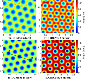
Figure 11. AFM topography images (2.5 μm × 2.5 μm) of Ti patterns (left side) obtained by DCMS depositions with SRCMs at two working gas pressure values (3 and 30 mTorr) and the TiO2 patterns resulting from their oxidation (right side). The height colour scale is the same for all images.
Download figure:
Standard image High-resolution image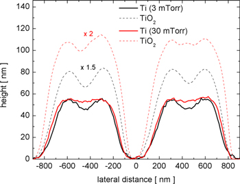
Figure 12. Height profiles of Ti and TiO2 (resulting from oxidation of Ti) patterns obtained by DCMS of Ti on SRCMs at two working gas pressure values.
Download figure:
Standard image High-resolution imageAs a result of pattern oxidation, the pattern height increases by a factor of 1.5 for the Ti pattern deposited by DCMS at a low working gas pressure (3 mTorr) and by a factor of 2 for the Ti pattern deposited by DCMS at a high working gas pressure (30 mTorr). The volume increasing factors observed in the oxidation of the Ti patterns obtained with SRCMs are slightly smaller than the factors observed in the oxidation of Ti patterns obtained with CPCMs. This may be explained by a larger lateral expansion of the patterns in the latter case (visible as a shrinking of the holes). Important changes of pattern surface topography as a result of oxidation were also observed for the Ti patterns obtained by HiPIMS depositions on SRCMs. These changes are illustrated in figure SI7 of the SI. For the patterns deposited at a low working gas pressure, an increase of the pattern height by a factor of 1.5 and an enhanced shrinkage of the holes has been noticed, while for the pattern deposited at a high working gas pressure it has been observed that there is no noticeable change in pattern height and a slight shrinkage of the holes.
The crystalline structure of the TiO2 2D patterns obtained with SRCMs has been investigated by XRD. The XRD patterns (figure 13) show formation of a rutile phase for the oxidized Ti patterns obtained by both DCMS and HiPIMS techniques working at low and high working gas pressure values. The broadening of the diffraction peaks determines values between 6 and 30 nm for the size of the nanocrystallites. For the patterns obtained by HiPIMS depositions, the value of gas pressure used in the depositions has a much stronger effect on the crystalline order of the oxidized patterns. Thus, the pattern obtained by thermal oxidation of the Ti patterns by HiPIMS deposition at a low working gas pressure is less crystalline. Moreover, the broad base of the diffraction peak at 2θ = 33.4° can be attributed to the formation of the sub oxide crystalline phases Ti2O3 and Ti2O [29].
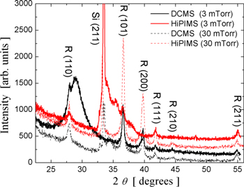
Figure 13. XRD pattern of TiO2 patterns obtained with SRCMs by DCMS and HiPIMS at two working gas pressure values.
Download figure:
Standard image High-resolution image3.4. Hydrophilicity and photocatalytic activity of TiO2 2D Ti patterns
The TiO2 surface becomes super hydrophilic (water contact angle less than 5°) when it is irradiated by UV light. This phenomenon is related to the photocatalytic activity of the TiO2 material and is attributed to the photocatalytic decomposition of either water or hydrophobic adsorbed molecules at Ti4+ photoreduced to Ti3+ sites, which are situated at the oxygen bridges on the surface [30]. As compared to the surfaces of uniform TiO2 films, we expect an enhancement of the effect of UV-light irradiation on the hydrophilicity of TiO2 patterns due to the effects of pattern topography on the water contact angle [9] and of the enhancement of the photocatalytic activity of the patterns. Indeed, all the TiO2 patterned surfaces described above showed a much faster decrease of the water contact angle when compared to the uniform TiO2 films obtained by the same deposition and oxidation techniques. Uniform TiO2 films were prepared by either DCMS or HiPIMS depositions of uniform Ti films on quartz substrates and then thermally oxidized, retaining the experimental parameters used in the 2D pattern fabrication.
Figure 14 shows the comparative variation of the water contact angle for a uniform TiO2 film (100 nm in thickness) and the TiO2/SiO2 patterns obtained by HiPIMS depositions at a low working gas pressure (3 mTorr) with a CPCM and an SRCM. Before UV irradiation, the patterns and film surfaces showed some degree of hydrophobicity (water contact angle around 90 degrees) due to either fully stoichiometric surfaces or adsorbed contaminant hydrocarbon molecules [31]. As a result of the UV irradiation, the water contact angle decreased much faster on the TiO2 patterned surfaces than on the uniform TiO2 films. All the TiO2 patterns described above showed similar variations of the water contact angle as a result of UV-light irradiation (see figure SI6 of the SI).
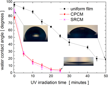
Figure 14. Variation of the water contact angle for a uniform TiO2 film and the TiO2/SiO2 2D patterns obtained by HiPIMS depositions at a low working gas pressure (3 mTorr) with a CPCM and a SRCM, respectively.
Download figure:
Standard image High-resolution imageThe photocatalytic activity of the TiO2 2D patterns towards decomposition of the MB molecules in an aqueous solution under visible light irradiation was investigated and compared with the activity of uniform TiO2 thin films obtained by the same deposition techniques and thermal oxidation. Figure 15 presents the variation of MB concentration in an aqueous solution during visible light irradiation of uniform TiO2 thin films and the TiO2/SiO2 patterns described above. As expected, the photocatalytic activity of the TiO2 patterns in visible light is higher than that of the uniform films. This may be a synergetic result of effects such as: (1) a better adsorption of visible light; (2) an increase of the effective area of the active TiO2 surface; (3) a longer lifetime of photo-generated charge carriers due to their spatial separation in pattern structures; and (4) a better absorption and diffusion of dye molecules on the patterned surfaces. However, the TiO2/SiO2 2D patterns fabricated by different techniques at different values of the sputtering gas pressure showed different photocatalytic activities. The patterns obtained with SRCMs are more active than the patterns obtained with CPCMs. This can be explained by the weak absorption of light on the latter patterns due to their small height (thickness). Also, the effective area of the pattern surfaces is much larger for the patterns obtained with SRCMs as compared to the patterns obtained by CPCMs. The AFM images indicate an effective area about two times larger for the patterns obtained with SRCMs than for the patterns obtained with CPCMs. The absorption of MB molecules is slightly better on the patterned TiO2 surfaces as compared to the uniform TiO2 film surfaces, a fact indicated by the decrease of MB concentration during the initial time of 5 min (prior to visible light irradiation), when the probes were kept embedded in the MB solution without light irradiation.

Figure 15. Variation of concentration of methylene blue (MB) aqueous solution as a result of irradiation with visible light of uniform TiO2 films and TiO2 patterns obtained by DCMS and HiPIMS depositions of Ti with CPCMs and SRCMs followed by mask lift-off and thermal oxidation.
Download figure:
Standard image High-resolution imageThe patterns produced by HiPIMS are more active than those produced by DCMS. This might be the effect of a more dense structure of the patterns produced by HiPIMS, which correspond to a lower density of charge carrier recombination sites. The pressure of the sputtering gas also had an effect on the pattern photocatalytic activity, a slightly better activity being observed for the patterns obtained at low pressure. This might also be an effect of a denser structure of the patterns obtained in sputtering depositions at a low sputtering gas pressure. For all the patterns, the rate of the photocatalytic decomposition of MB molecules showed a large decrease during the first 20 min of visible light irradiation from a large initial value to a value that then remained approximately constant afterwards. For the most active TiO2 patterns deposited by HiPIMS on SRCMs, the MB decomposition reaction rate decreased from the initial value of 4.5 · 1015 molecule/s to a value of about 1.6 · 1014 molecules/s. For the uniform film surfaces, the MB decomposition reaction rate showed a continuous decrease from the initial value of 8.6 · 1014 molecules/s to 9 · 1013 molecules/s after 120 min of irradiation. Considering the effective area of the irradiated probes and a density of surface reaction sites of 2.2 · 1016 sites/cm2 [32], we estimated turnover number values (after 120 min of irradiation) of around 60 and 26 for the TiO2 patterns obtained by HiPIMS deposition with SRCMs and the uniform film obtained by DCMS deposition, respectively. These values are larger than the values reported for thin anatase TiO2 films deposited by reactive DCMS [32].
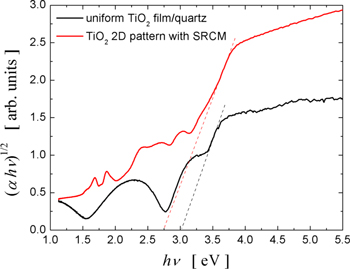
The best photocatalytic activity was obtained by the pattern fabricated by HiPIMS deposition at a low working gas pressure (3 mTorr) with an SRCM. The XRD data for this latter pattern showed a less crystalline order with the formation of sub oxide crystalline phases. This is expected to determine a decrease of the photocatalytic activity of this pattern. However, incomplete oxidation of this pattern and formation of sub oxide crystalline phases may increase the absorption of visible light due to a decrease of the energy bandgap. This is proved by the results of the light absorption spectroscopy measurements performed for the TiO2 uniform film and 2D pattern fabricated on quartz substrate by HiPIMS deposition of Ti followed by thermal oxidation. The patterned TiO2 sample showed a much better absorption in visible light than the uniform film. The Tauc plots presented in figure 16 indicate an energy bandgap of 3 eV for the uniform film and 2.7 eV for the patterned surface.
Figure 16. The Tauc plots of the TiO2 pattern deposited by HiPIMS deposition at a low sputtering gas pressure on quartz substrate with an SRCM and of the TiO2 uniform film obtained by the same method.
Download figure:
Standard image High-resolution image
Such an important reduction of the bandgap may be due to the effect of the formation of Ti-terminated surfaces on the TiO2 2D nanopatterns. Recent investigations showed that an important reduction of bandgap energy at a standard anatase TiO2 surface can be achieved by thermal treatment in oxygen to generate a Ti-terminated anatase surface phase on the stoichiometric oxygen-terminated surface [33]. Nanostructured and reduced TiOx (x < 2) could be a good visible light photocatalytic material provided the charge carrier recombination probability is maintained low [34]. However, all the patterns studied in this work showed a relatively good transparency, which is an indication of the complete oxidation of Ti patterns. This is proved by optical microscopy images obtained in reflected light on TiO2/SiO2 patterns on Si and in transmission light on TiO2/SiO2 patterns, which are presented in figures SI8 and SI9 of the SI material. A slight reduction of the bandgap energy can be attributed to the quantum confinement of charge carriers in the nanostructured TiO2 patterns and thin films. The Brus model of first excitonic energy in a semiconductor cluster foresees a reduction of bandgap energy with about 0.1 eV for TiO2 nanoparticles with a diameter of 5 nm [35].
4. Conclusion
TiO2/SiO2 2D nanopatterned surfaces were fabricated by magnetron sputtering depositions of Ti on colloidal masks on Si and quartz substrates, followed by the lift-off of the colloidal masks and ending with thermal oxidation. Closely-packed colloidal masks were obtained by spin coating deposition of a monolayer of PS beads with a diameter of 500 nm. The patterns obtained with these masks reproduced the triangular shape of the opening spaces of the close-packed colloidal masks and their height did not exceed 10 nm because the deposited films quickly filled the opening spaces of the mask. To increase the opening spaces of the colloidal mask, size-reduced colloidal masks (PS beads with their diameter reduced to about 400 nm) were fabricated by RIE in oxygen plasma of the closely-packed colloidal masks. The reactive etching increased the opening spaces of the masks, which determined the deposition of patterns with a much larger height. These latter patterns can be described as relatively uniform films with hexagonal hole lattices left by the PS beads of the etched masks. The two sputtering deposition techniques used in the present work, i.e. dc magnetron sputtering and high power impulse magnetron sputtering, gave different results in terms of pattern shape, size and structure. Compared to dc magnetron sputtering, the high power impulse magnetron sputtering produced more compact and well-defined 2D nanopatterns because of a higher energy and ionization ratio of the sputtered atoms. The pressure of the sputtering gas had a strong effect on the density and compactness of the patterns. At a high pressure (30 mTorr), the sputtered atoms have low energies and a wider distribution of incidence angle values on the growing films, which determined the isotropic depositions of the low-density films and patterns. In this case, the colloidal masks played the role of templates for columnar growth. At a low sputtering gas pressure (3 mTorr), the sputtered atoms were more energetic and came preponderantly from the direction of the sputtering target, which determined anisotropic depositions of smooth and compact films and patterns. In this case, the open spaces of the colloidal masks were filled much more slowly and the height of the patterns was larger.
The substrates with the Ti 2D nanopatterns were thermally oxidised in pure oxygen atmosphere to obtain TiO2/SiO2 2D nanopatterned surfaces. Thermal oxidation determined the formation of patterns with a polycrystalline rutile structure and an increased volume (compared to the volume of the Ti patterns). An estimation based on the conservation of the number of Ti atoms in the patterns indicated an increasing factor of 1.76 for the transformation of Ti in rutile TiO2. Topography AFM images of the patterns taken before and after thermal treatment revealed an increase in pattern height with a factor ranging between 1.5 and 2.7. A larger increase of volume was noticed for the oxidation of low density patterns deposited by dc magnetron sputtering at a high sputtering gas pressure.
The effect of UV light irradiation on the hydrophilicity of the 2D patterned TiO2/SiO2 surfaces has been investigated by measurements of the water contact angle. Compared to the surface of uniform TiO2 films prepared by the same techniques, all patterned surfaces became superhydrophilic much faster by UV irradiation. The photocatalytic activity of the TiO2 patterned surfaces was investigated by measurement of the decomposition rate of MB in aqueous solutions under visible light irradiation of the patterned surfaces. The photocatalytic activity of the TiO2 patterns in visible light was higher than that of the uniform TiO2 films obtained by the same techniques. The patterns obtained with size-reduced colloidal masks were more active than the patterns obtained with close-packed colloidal masks. The patterns produced by high power impulse magnetron sputtering were more active than those produced by dc magnetron sputtering. Also, the patterns obtained by depositions at a low sputtering gas pressure had a slightly better activity than the patterns obtained by depositions at a high sputtering gas pressure. The higher photocatalytic activity of the patterned TiO2 surfaces in visible light has been attributed to an important reduction of the bandgap energy of TiO2 in patterns.
Acknowledgments
This work has been supported by the Romanian National Plan for Research, Development and Innovation, grant JOINT RESEARCH PROJECTS PN-II-ID-JRP-2012-RO-FR-0161.