


Abstract
Recently metrological atomic force microscopes (metrological AFMs) have been used for surface roughness measurements. The National Metrology Institute of Japan (NMIJ), AIST, provides a profile surface roughness calibration service using a metrological AFM based on ISO 19606:2017. This international standard requires evaluation of probe-tip diameter D and error in roughness measurements by using a standard plate with needle-shaped spikes before conducting surface roughness measurements. However, the conventional standard plate has several problems: (1) the needle-shaped spikes are too high, (2) the distance between spikes is too long, and (3) the spike curvature radius is not small enough, compared with AFM probe-tip size, which may lead to considerable uncertainty derived from probe-tip error evaluation. This study examined a new type of commercially-available standard plate as a candidate for probe-tip diameter evaluation. It features lower spike height and shorter distance between spikes in order to avoid probe-tip wear caused by repeated scanning. This study demonstrated that the overestimated uncertainty derived from probe-tip error evaluation can be corrected by using the new standard plate.
1. Introduction
Atomic force microscopes, as well as stylus and optical instruments, have been used to measure surface roughness to achieve sufficiently high quality in fabrication processes, such as, thin film formation and material surface treatment [1–7]. Several tip radius evaluation methods have been proposed for reliable metrology [8–10]. In particular, metrological atomic force microscopes (metrological AFMs) are used to enhance the reliability of roughness measurement results [11–14]. The National Metrology Institute of Japan (NMIJ), AIST, provides a profile surface roughness calibration service using a metrological AFM based on ISO 19606: 2017 [15–17].
This international standard requires probe-tip error evaluation by using a probe-tip diameter evaluation standard plate before conducting surface roughness measurements of a specimen. As a measured probe-tip diameter D contains profile information of both an AFM probe-tip and a standard plate used for probe-tip diameter evaluation [15–17], the measured D is overestimated, compared with the true diameter of AFM probe-tip. A probe-tip diameter evaluation standard plate needs to have spikes that are as sharp as possible.
It is necessary to evaluate probe-tip diameter D and error in roughness measurements [15–17] using a standard plate with needle-shaped spikes [18] before conducting surface roughness measurements. The conventional standard plate, however, has several problems as described later. This study examined a different type of commercially-available standard plate as a candidate [19] for the probe-tip diameter evaluation, which features lower spike height and shorter distance between spikes to avoid tip wear caused by repeated scanning. The standard plate candidate is used in studies related with dimensional measurement by AFM or other probe measurement techniques [20–28], for instance, an international round robin test of the size of nano-particles [20]. However, uncertainty evaluation in surface roughness measurements using the standard plate candidate has not been conducted yet. It is helpful for users if the standard plate candidate can be used for the probe-tip error evaluation based on ISO 19606: 2017 [15]. In this study, surface roughness is measured for eight types of specimens, all of which were used in the previous studies described in [16] and [17].
2. Measurement conditions
2.1. Instrument
The metrological AFM used for roughness measurements in this study is the same as that used in the previous studies [16, 17]. It is an SI (International system of units)-traceable instrument since laser interferometers are installed on its x, y and z axes. By using a metrological AFM, the calibration procedure of x, y and z scan axes, using a certified calibration standard stipulated in ISO 19606: 2017 [15] is unnecessary.
2.2. Method to determine criteria for probe-tip error [15–17]
Figure 1 shows the probe-tip evaluation sequence. Ra and RSm are the arithmetical mean roughness and mean width of roughness profile elements, respectively. First, preliminary roughness measurements of a specimen are carried out to obtain preliminary Ra and RSm. The preliminary values are necessary in the probe-tip judgement procedure. Next, part of the probe-tip diameter evaluation standard plate is measured. The cross section of a spike profile at 10 nm below its top in Z direction is obtained and D is calculated from the cross section as a probe-tip diameter based on '10.3 Evaluation of probe-tip diameter' and 'Annex A' of ISO 19606: 2017. The desired value of D, the diameter of the cross section of the AFM probe tip for measuring surface roughness with sufficient accuracy, is expressed using the model below. The model assumes that the specimen surface profile is sinusoidal with a cycle of RSm given by equation (1):
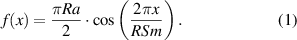

Figure 1. Probe-tip evaluation sequence [15].
Download figure:
Standard image High-resolution imageIn this case, Ra is expressed as follows:
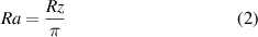
where Rz is the maximum height of roughness profile.
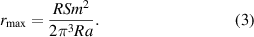
Equation (2) gives a value between a triangle wavefront and a rectangular wavefront, that is often close to the real value of the specimen. The tip of a probe is assumed to be a spherical surface with a radius of curvature r, which is desirable if it can reach the bottom parts of the roughness profile. Therefore, a tip with a radius greater than the maximum radius of the inscribed circle (r = rmax) cannot reach the bottom of the roughness profile and is not suitable for roughness measurements. A tip with r less than or equal to rmax is considered acceptable. Based on the above model, rmax is given by
Then, Dmax, D value corresonding to rmax, is expressed as follows:

However, for sharp tips where r is less than 10 nm, must be used. Ra is a constant, whose value is a preliminary value obtained in the first step of figure 1, and RSm is a variable in the range of 0.04 µm to 2.5 µm. Based on Annex B of ISO 19606: 2017 [15], if D is less than Dmax/2 (5% criterion), the Ra measurement error is expected to be less than 5%, and if D is between Dmax/2 and Dmax (20% criterion), it is expected to be less than 20%.

2.3. Standard plate used for probe-tip diameter evaluation
Table 1 shows the specifications of the standard plates used for probe-tip diameter evaluation in the previous studies [16–18] and in this study [19]. Figures 2(a)–(c) show a schematic drawing of the probe-tip diameter evaluation standard plate used in the previous studies [16–18], a thermal field emission scanning electron microscope (FE-SEM) (HITACHI S4300-SE, acceleration voltage: 2.0 kV) image of a top view of the standard plate, and an SEM image of a birds eye view of the standard plate, respectively. The standard plate has a number of needle-shaped spikes and has the advantage of being intuitive and easy to use since it is similar in shape to a knife edge used in conventional stylus-type roughness measurement instruments. However, several drawbacks were identified in the previous studies. (1) Needle-shaped spikes are too high, compared with the surface roughness of a specimen, which in general ranges from 300 nm to 500 nm. Probe tip might be damaged during the probe-tip diameter evaluation conducted before roughness measurements of a specimen. We cannot know a coordinate of a certain needle-shaped spike preliminarily, therefore the AFM measurement capturing whole shape of the needle-shaped spike is needed. At this time, AFM probe-tip must scan on the slope portion of the spike. The AFM-probe control along vertical axis tends to be unstable on the steep slope due to the interference between the probe-tip (having finite cone angle) and the spike. Therefore, there is a possibility that it results in higher tip wear. Additionally, there are broken spikes in the needle-shaped spikes, thus the spike measurement not necessarily completes at one time. Figure 3 shows metrological AFM images of the standard plate used for probe-tip diameter evaluation. Figure 3(a) is an example of successful approach of a probe-tip to the standard plate, and figure 3(b) is an example of failure to approach the same probe-tip to the standard plate. (2) The distance between spikes is approximately 2.12 μm, which is too long. Several AFM images are needed for positioning of the standard plate, which takes a long time. (3) The spike curvature radius is approximately 10 nm, which is not small enough, compared with AFM tip size. The probe-tip diameter might be overestimated if the curvature radius of a spike is not sufficiently small.
Table 1. Specification of the standard plate used for probe-tip diameter evaluation.
| Manufacturer | Product number | Distance between any two nearest neighboring spikes (nm) | Spike base (nm) | Spike height (nm) | Spike angle (degrees) | Spike curvature radius (nm) | Reference |
|---|---|---|---|---|---|---|---|
| NT-MDT Spectrum Instruments | TGT1 | 2120 | — | 300–500 | 50 | 10 | [16–18] |
| MICROMASCH® | PA01 | (100–200) | 50–100 | 50–150 | — | Less than 5 (minimum) | [19–28] This study |

Figure 2. (a) Schematic drawing of a probe-tip diameter evaluation standard plate used in the previous studies [14–16]. (b) Thermal field emission scanning electron microscope (FE-SEM) (HITACHI S4300-SE, acceleration voltage: 2.0 kV) image of a top view of the standard plate. (c) SEM image of a birds eye view of the standard plate. (a) Reprinted from [17], Copyright (2019), with permission from Elsevier.
Download figure:
Standard image High-resolution image
Figure 3. Metrological AFM images of the standard plate (TGT1) used for probe-tip diameter evaluation. (a) Example of a successful approach of a probe-tip to the standard plate. (b) Example of a failure to approach the same probe-tip to the standard plate.
Download figure:
Standard image High-resolution imageFigures 4(a)–(c) show a schematic drawing of the top view of the probe-tip diameter evaluation standard plate used in this study [19], a thermal FE-SEM (acceleration voltage: 20.0 kV) image of a top view of the standard plate, and an SEM image of a birds eye view of the standard plate, respectively. This standard plate is composed of sharp pyramidal nanostructures. The pyramids are triangular with a base of 50 nm to 100 nm in length and their height ranges from 50 nm to 150 nm. The curvature radius of the sharpest tips is below 5 nm.

Figure 4. (a) Schematic drawing of the top view of the probe-tip diameter evaluation standard plate used in this study [19]. (b) Thermal FE-SEM (acceleration voltage: 20.0 kV) image of a top view of the standard plate. (c) SEM image of a birds eye view of the standard plate.
Download figure:
Standard image High-resolution image2.4. Specimens
Table 2 shows the specifications of the specimens for roughness measurements. All of the eight specimens were used for roughness measurements in the previous studies [16, 17]. As a result of the probe-tip error evaluation in one of the previous studies [16], Specimen 2 alone was judged to be suitable for roughness measurements with an error of 20%. In this study, therefore, measurement results of Specimen 2 are mainly reported.
Table 2. Specification of the specimens [16, 17].
| Specimen No. | Specimen | Manufacturer | Product number | Reference | Evaluation result of probe-tip diameter and error in roughness measurement in the previous studies |
|---|---|---|---|---|---|
| 1 | Silicon wafer | Shin-Etsu Chemical Co, Ltd | CZ-P <100> | [17] | 5% |
| 2 | Flat aluminum total reflection mirror | SURUGA SEIKI CO, Ltd | S01-20-3 T | [16] | 20% |
| 3 | Indium tin oxide (ITO) thin film | GEOMATEC CO, Ltd | 0007 | [16] | 5% |
| 4 | Indium tin oxide (ITO) thin film | GEOMATEC CO, Ltd | 0005 | [16] | 5% |
| 5 | TipCheck sample | Aurora NanoDevices Inc | TIP001 | [16] | 5% |
| 6 | Gauge block | Mitutoyo Corporation | 613614–02 | [16] | 5% |
| 7 | Roughness standard | SiMETRICS GmbH | RnS 40 | [16] | 5% |
| 8 | Roughness standard | SiMETRICS GmbH | ARS f1 | [17] | 5% |
2.5. Cantilever probes
The standard silicon cantilever probes (OMCL-AC160TS, Olympus Co, Ltd) used in this study are the same as those used in the previous studies, featuring a spring constant of approximately 42 and resonance frequency of approximately 300 kHz. Since the combination of the specimens and the cantilever probes in this study is the same as that in the previous studies, the preliminary Ra and preliminary RSm of the previous studies are used in this study.

2.6. Roughness measurements
Table 3 shows roughness measurement conditions of each specimen. All measurement conditions in this study are the same as those in the previous studies [16, 17]. The reason why the number of picture elements is 512 (Y) × 16 (X) is as follows. The number of picture elements in the fast-scanning direction and in the slow-scanning direction is selected from 256 pixels to 512 pixels and from 10 pixels to 512 pixels, respectively, based on '11 Roughness measurements of specimen' in ISO 19606: 2017 [15]. Furthermore, in the last procedure of the roughness measurements, Sa (arithmetical mean height of the scale limited surface) featuring the number of picture elements of 512 (Y) × 512 (X) at the fifth measuring point for all eight specimens were obtained in the previous studies. All Sa were in the ranges of the uncertainty of all Ra. Furthermore, when measurements with the number of picture elements of 512 × 512 are repeated, as shown in of reference [16], the probe-tip is worn, the values of roughness become smaller, and the expanded uncertainties increased. Therefore, it can be considered that the number of picture elements of 512 (Y) × 16 (X) is suitable in this study. One probe is used per specimen. The roughness of Specimen 1, Specimen 2, Specimen 3 ... Specimen 8 is measured in this order. The measurement order of the five measurement points in one sample is randomly selected. Two repeated measurements at each measuring point are performed continuously. This is because the scanner of the metrological AFM in our institute cannot be positioned again at the same measuring point. Ra, RSm and D are calculated by combining the roughness analysis module and the particle analysis module of the Scanning Probe Image Processor (from Image Metrology A/S) [29]. A λc filter is set to one fifth of each scanning range.
Table 3. Roughness measurement conditions of each specimen [16, 17].
| Specimen No. | Evaluation length (μm × μm) | Scanning speed (nm s−1) | Number of picture elements | Number of measuring points | Repetition number at each measuring point |
|---|---|---|---|---|---|
| 1 | 1 × 1 | 100 | 512 × 16 | 5 | 2 |
| 2 | 2 × 2 | 400 | 512 × 16 | 5 | 2 |
| 3 | 2 × 2 | 400 | 512 × 16 | 5 | 2 |
| 4 | 5 × 5 | 500 | 512 × 16 | 5 | 2 |
| 5 | 5 × 5 | 500 | 512 × 16 | 5 | 2 |
| 6 | 10 × 10 | 1000 | 512 × 16 | 5 | 2 |
| 7 | 20 × 20 | 1200 | 512 × 16 | 5 | 2 |
| 8 | 20 × 20 | 1200 | 512 × 16 | 5 | 2 |
3. Measurement results and discussion
3.1. Evaluation of probe-tip diameter
Figure 5(a) shows a 3D rendering image of a metrological AFM image of the standard plate captured before surface roughness measurements of Specimen 2. The scan area is 320 nm (Y) × 320 nm (X). The number of picture elements is set at 512 pixels (Y) × 512 pixels (X) based on '10.3 Evaluation of probe-tip diameter' in ISO 19606: 2017 [15]. Figure 5(b) is a gradient norm image of figure 5(a). Figure 5(c) is a top view of figure 5(a). The numbers in figure 5(c) indicate spike positions where the cross sections of the spikes are profiled at 10 nm below their tops in the Z direction and the D are calculated. Figure 5(d) shows an example of cross-sectional area (blue color) at 10 nm below its top in Z direction. When each D is calculated, the area of interest (AOI) is limited in a way to contain just one spike as shown in figure 5(d). Table 4 shows the calculation results of D. The calculated results range from 30.4 nm at Position 2 to 37.0 nm at Position 8. The minimum value of 30.4 nm is selected as D for Specimen 2. In a previous study, D for Specimen 2 was approximately 43.2 nm [16]. The new probe-tip diameter evaluation standard plate makes it unnecessary to adjust the AFM probe tip onto a certain spike. This enables us to measure many spikes at once, which may contribute to lower tip wear, and also to choose a minimum value (taken from the sharpest spike of the standard plate) so as to estimate optimum D. By using the new probe-tip diameter evaluation standard plate, the overestimation of D is corrected. For the other seven specimens in this study, D are found to range from 21.2 nm to 38.2 nm.
Table 4. Calculation results of probe-tip diameters, D.
| Spike position No. | Probe-tip diameter, D (nm) | Area (nm2) | Minimum Z (nm) | Maximum Z (nm) |
|---|---|---|---|---|
| 1 | 35.3 | 978.04 | −58.02 | −48.06 |
| 2 | 30.4 | 727.45 | −63.04 | −53.08 |
| 3 | 34.2 | 920.78 | −57.71 | −47.75 |
| 4 | 36.6 | 1052.5 | −65.09 | −55.13 |
| 5 | 33.4 | 875.68 | −69.15 | −59.18 |
| 6 | 33.4 | 873.72 | −64.78 | −54.82 |
| 7 | 35.5 | 986.66 | −64.67 | −54.70 |
| 8 | 37.0 | 1075.7 | −76.14 | −66.17 |
| 9 | 34.3 | 923.92 | −71.66 | −61.69 |
| 10 | 31.4 | 776.47 | −77.61 | −67.64 |
| 11 | 35.5 | 989.02 | −76.18 | −66.21 |
| 12 | 32.9 | 849.02 | −74.90 | −64.94 |
| 13 | 33.6 | 888.62 | −78.77 | −68.72 |

Figure 5. (a) A 3D rendering image of a metrological AFM image of the standard plate used for probe-tip diameter evaluation. (b) The Z gradient norm image of (a). (c) Top view of (a): The numbers indicate spike positions where the cross sections of the spikes profiled at 10 nm below their tops in the Z direction and the D were calculated. (d) An example of cross-sectional area (blue color) at 10 nm below its top in Z direction.
Download figure:
Standard image High-resolution image3.2. Evaluation of error in roughness measurements
Figure 6 shows a D-RSm map for the probe-tip error evaluation and the evaluation results in this study and one of the previous studies. Detailed information of D-RSm map is described in the previous studies [15, 16]. For Specimen 2, the preliminary Ra of 1.4 nm and RSm of 80.0 nm used in the previous study are also used in this study. The solid and dotted lines represent 20% and 5% criteria, respectively, and the open and solid circles show the results of the previous study [16] and this study, respectively. The open circle is below the solid line. This indicates that the probe-tip can be used for roughness measurements with an error of less than 20% of Ra. The solid circle is below the dotted line. This demonstrates that the probe-tip is capable of performing roughness measurements with less than 5% error. The new standard plate is found to be effective in improving the evaluation of probe-tip error. For the other seven specimens as well, the probe-tip error evaluation results demonstrate that their surface roughness is also measured with errors less than 5%.

Figure 6. A D-RSm map for the probe-tip error evaluation to measure roughness of Specimen 2. Adapted from [16], Copyright (2015), with permission from Elsevier.
Download figure:
Standard image High-resolution image3.3. Roughness measurement results
Figure 7 shows the results of Specimen 2 roughness measurements and their uncertainty evaluations in this study and a previous study [16]. The diamonds and error bars indicate Ra and expanded uncertainty U95, respectively. Table 5 shows major sources of uncertainty in roughness measurements of each specimen and their contributions to the combined standard uncertainty. In Specimen 2, the expanded uncertainty in this study dropped to half that in the previous study because the uncertainty derived from the probe-tip error evaluation decreased. In addition, Ra values are found to be within the expanded uncertainties both in this study and the previous study, which demonstrates the consistency of the measurement results.
Table 5. Major sources of uncertainty in surface roughness measurements of all specimens and their contributions to the combined standard uncertainty [16, 17].
| Contribution to the combined standard uncertainty, u (nm) | |||||||||||||||||
|---|---|---|---|---|---|---|---|---|---|---|---|---|---|---|---|---|---|
| Specimen No. | 1 | 2 | 3 | 4 | 5 | 6 | 7 | 8 | |||||||||
| Major source of uncertainty | Previous study [17] | This study | Previous study [16] | This study | Previous study [16] | This study | Previous study [16] | This study | Previous study [16] | This study | Previous study [16] | This study | Previous study [16] | This study | Previous study [17] | This study | |
| Interferometer nonlinearity | 0.07 | 0.07 | 0.07 | 0.07 | 0.07 | 0.07 | 0.07 | 0.07 | 0.07 | 0.07 | 0.07 | 0.07 | 0.07 | 0.07 | 0.07 | 0.07 | |
| Probe-tip error evaluation | 0.005 | 0.004 | 0.16 | 0.04 | 0.04 | 0.04 | 0.20 | 0.13 | 0.24 | 0.24 | 0.30 | 0.34 | 1.8 | 1.8 | 3.0 | 3.0 | |
| Non-uniformity of surface roughness of a specimen | Negligible | Negligible | 0.03 | 0.04 | 0.03 | 0.02 | 0.14 | 0.11 | 0.09 | 0.09 | 0.74 | 0.82 | 1.5 | 0.7 | 1.6 | 2.9 | |
| Interferometer resolution | 0.02 | 0.02 | 0.02 | 0.02 | 0.02 | 0.02 | 0.02 | 0.02 | 0.02 | 0.02 | 0.02 | 0.02 | 0.02 | 0.02 | 0.02 | 0.02 | |
| Repeatability of measurement | Negligible | Negligible | 0.01 | Negligible | 0.01 | Negligible | Negligible | 0.01 | Negligible | Negligible | Negligible | 0.03 | 0.06 | 0.03 | 0.12 | 0.05 | |

Figure 7. Roughness measurement results and expanded uncertainties of Specimen 2 in this study and a previous study [16].
Download figure:
Standard image High-resolution image
Table 6 shows roughness measurement results of each specimen. For Specimens 1, 3, 4 and 5, Ra and U95 remain almost unchanged from the previous studies. For Specimens 6, 7 and 8, Ra in this study is slightly larger than that in the previous studies. There is a possibility that, due to less probe-tip wear realized by using the new probe-tip diameter evaluation standard plate, Ra increases slightly. Further investigations concerning tip wear during probe-tip error evaluation procedures are necessary. The increase in the expanded uncertainty in roughness measurements of Specimen 8 in this study is attributed to larger uncertainty derived from non-uniformity of its surface roughness as shown in table 5. The number of measuring points was 5 in previous [15] and this studies based on ISO 19606: 2017. However, it might be necessary to increase the number of measuring points to evaluate the uncertainty derived from non-uniformity of surface roughness of a specimen more precisely.
Table 6. Roughness measurement results of each specimen [16, 17].
| Previous studies [16, 17] | This study | |||
|---|---|---|---|---|
| Specimen No. | Measurement result, Ra (nm) | Expanded uncertainty, U95 (nm) | Measurement result, Ra (nm) | Expanded uncertainty, U95 (nm) |
| 1 | 0.17 | 0.14 | 0.15 | 0.14 |
| 2 | 1.4 | 0.4 | 1.3 | 0.2 |
| 3 | 1.5 | 0.2 | 1.5 | 0.2 |
| 4 | 4.5 | 0.5 | 4.4 | 0.4 |
| 5 | 8.6 | 0.6 | 8.4 | 0.5 |
| 6 | 10.4 | 2.1 | 11.7 | 2.3 |
| 7 | 61.5 | 4.6 | 63.7 | 4.2 |
| 8 | 102.5 | 6.8 | 103.8 | 9.1 |
3.4. Discussion
Use of the new probe-tip diameter evaluation standard plate reduces the uncertainty in probe-tip error evaluation. The 5% criterion and 20% criterion in evaluation of error in roughness measurements were experimentally determined based on round robin test results [15, 16]. The possibility to set a 3% criterion is suggested by the Ra measurement results for a specimen with Ra = 20 nm [15]. In order to further decrease uncertainty derived from probe-tip error evaluation, it is necessary to obtain successful results in round robin tests so as to be able to propose a criterion below 5%.
In the measurements of smaller roughness, the uncertainty derived from instruments, such as an interferometer, becomes increasingly dominant as shown in table 5. A new metrological AFM is under development to realize roughness measurements with smaller uncertainties [30]. It has been demonstrated that the metrological AFM under development is capable of reducing the Z-axis component of the thermal drift rate to about 1 nm h−1 while an AFM probe gets close to the surface in a stabilized measurement environment [30]. The use of a low-noise AFM operating at low relative humidity was also reported for the purpose of realizing surface roughness metrology in sub-nanometer order [31]. Furthermore, metrological AFMs are expected to be applied to line edge roughness (LER) measurements as well as surface roughness measurements. A metrological AFM with a tip-tilting mechanism has been developed [32] and is used for LER metrology [33].
4. Outlook and conclusion
In this study, a different type of commercially-available standard plate as a candidate was used, featuring lower spike height and eliminating the need for aligning the position of the AFM probe-tip onto a certain spike. This standard plate is found to be effective in reducing uncertainty caused by probe-tip error evaluation since many spikes are measured simultaneously and the sharpest one can be selected. Therefore, the possibility of adopting a 5% criterion will be increased. The authors plan to evaluate uncertainty in measurement of arithmetical mean height of the scale limited surface, Sa [7, 17], and other parameters [12, 13] in addition to Ra in the future.
Acknowledgments
Part of this study was supported by Nippon Sheet Glass Foundation for Materials Science and Engineering and The Precise Measurement Technology Promotion Foundation.