
Abstract
Antimony selenosulfide (Sb2(S,Se)3) solar cells have attracted great attention due to their tunable optoelectronic properties, ease of preparation and low toxicity. However, the harmful intrinsic defect density and internal nonradiative recombination of Sb2(S,Se)3 hinder its practical usage. In this work, a facile additive approach is explored to modify the Sb2(S,Se)3 solar cell efficiency by using tetrabutylammonium iodide (TBAI). After applying a certain amount of TBAI into the Sb2(S,Se)3 precursor solution, the film surface presents lower cracks and roughness than that of the pristine sample. It also increases its hydrophobicity and n-type nature revealed by contact angle and work function measurements. Moreover, the incorporation of TBAI during the formation of the Sb2(S,Se)3 layer improves the quality of the film effectively suppresses its defect trap density, which manifests as a reduction in charge recombination and enhancement of the power conversion efficiency (PCE) when incorporated into solar cells. The fabricated device with 0.62 mol% of TBAI shows the highest PCE (8.87%) and high stability without encapsulation, maintaining about 91% of its initial efficiency after 60 d in air. The results provide a feasible strategy to the ongoing progress of reliable Sb2(S,Se)3 devices.
Export citation and abstract BibTeX RIS

Original content from this work may be used under the terms of the Creative Commons Attribution 4.0 license. Any further distribution of this work must maintain attribution to the author(s) and the title of the work, journal citation and DOI.
1. Introduction
Antinomy-based materials are particularly attractive for photovoltaic applications because of the good light harvesting properties, low cost, non-toxic and environmentally friendly nature [1–4]. Notably, solar cells based on Sb2(S,Se)3 alloys have received growing interest recently because of the tunability of their optical bandgap energy in the range of 1.1–1.7 eV by modulating the composition ratio of Se/(Se + S) [5]. This chemical modulation causes a considerable rise in the power conversion efficiency (PCE) up to 10.7% [6].
The growth of high-crystallinity absorber films with a minimum bulk defect formation, compact morphology and excellent optoelectronic properties is one of the most crucial issues in the final PCE enhancement of Sb2(S,Se)3 solar cells. Several deposition routes such as chemical bath deposition [7], vapor transport deposition [8], thermal evaporation [9], and close-space sublimation [10] have been extensively reported in the literature. Nevertheless, the hydrothermal process [11] has recently emerged as a viable solution technique. Although this deposition is susceptible to the presence of cracks, it is possible to adjust the film morphology and crystallinity by controlling the nucleation growth and/or reaction rate directly into the hydrothermal solution, or by post-deposition treatment [12–15]. Numerous efforts have been addressed to the processing of high-quality Sb2(S,Se)3 films, including additive engineering [13], interfacial engineering [14], crystal orientation manipulation [15] and solvent-assisted deposition [16]. Most of these studies are based on post-treatments of Sb2(S,Se)3 films through post-selenization/sulfidation with SeS2 or Se powder [17] or solution post-treatment with organic chloride and potassium iodide [6, 18].
Regarding additive engineering, Zhao et al [6] implemented a second hydrothermal process by using NaF, KF, RbF and CsF as additives of the previously synthesized Sb2(S,Se)3 films. They found that the post-treated films with an aqueous solution of NaF exhibit a mild S/Se gradient combined with passivated and reduced defects along the film, resulting in the record PCE of 10.7%. Li et al [19] found that by introducing an inorganic additive such as NHF4 in the hydrothermal solution, the surface of the CdS used as electron transport material is modified while a favorable band gradient of the Sb2(S,Se)3 film is created. Similarly, it has been demonstrated that using zeolite as an additive improves the compactness and reduces the presence of pinholes in the Sb2(S,Se)3 film, increasing the PCE of the devices.
Quaternary-ammonium cations, i.e. ethyl- and butyl-, have been successfully investigated as additives in the synthesis of conductive polymers [20] and inorganic/organic perovskites [21, 22], with beneficial effects on film quality, morphology and grain boundary passivation. For instance, by applying a low concentration of additives, such as methylammonium formate [23], ethylammonium and tetrabutylammonium iodide (TBAI) [24] in the precursor solution, the perovskite film is obtained with high-quality and surface coverage without affecting the crystal structure. The enhancement in the crystallinity of perovskite film, in turn leads to a superior photovoltaic performance. Moreover, TBAI has been used as a post-treatment method to passivate surface defects in perovskite solar cells [25]. Even though TBAI is gaining increased popularity as additive for perovskite solar cells through controlling the crystal growth process and suppressing the formation of undesirable defect states, there are currently no reports that explore the use of TBAI as additive in the crystallization process of Sb2(S,Se)3 films.
In this contribution, the impact of adding an optimal concentration of TBAI into the hydrothermal precursor solution of Sb2(S,Se)3 is investigated. The corresponding incorporation results in a smooth surface of the Sb2(S,Se)3 layer with few cracks and reduced work function, indicating a more n-type nature. It is also found that after adding TBAI, the trap density and charge recombination process are efficiently reduced in the Sb2(S,Se)3 layer. Consequently, the champion device using a cell architecture of fluorine-doped tin oxide (FTO)/c-TiO2/c-CdS/Sb2(S,Se)3 with TBAI/spiro-OMeTAD/Au exhibits the highest PCE of 8.87%, retaining nearly 91% of the initial performance after 60 d under ambient conditions.
2. Experimental section
2.1. Hydrothermal deposition
The FTO substrates were cleaned by successive ultrasonication in neutral detergent, ethanol, deionized (DI) water, and 2-propanol, and dried with compressed air. These substrates were exposed under UV light for 30 min to remove remnant organic residues. The TiO2 and CdS compact layers, c-TiO2 and c-CdS, respectively, were deposited sequentially according to previous literature [26]. The antimony selenosulfide films were growth by hydrothermal route from a precursor solution containing 20 mM antimony potassium tartrate trihydrate (Sigma-Aldrich, ⩾99%), 80 mM sodium thiosulfate pentahydrate (Sigma-Aldrich, ⩾99.5%), and 4.5 mM seleneourea (Sigma-Aldrich, 98%) dissolved in 40 ml DI water. Then, the proper amount of TBAI (Sigma-Aldrich, 98%) was incorporated into the above solution to obtain the desired molar ratios with respect to the Sb content. After that, the precursor solution was poured into the Teflon liner with the FTO substrates and placed in an electric oven at a temperature of 135 °C for 110 min. The as-deposited Sb2(S,Se)3 films were transferred into a glove box filled with nitrogen, placed on a hot plate at 330 °C for 20 min and cooled down to room temperature.
2.2. Device fabrication
To complete the device fabrication, a spiro-OMeTAD solution [26] was spin-coated at 3000 rpm for 30 s, and annealed in air at 100 °C for 10 min. Later, Au electrodes were thermally evaporated. In the case of space-charge limited current (SCLC) measurements, a phenyl-C61-butyric acid methyl ester layer was spin-coated on the Sb2(S,Se)3, followed by the thermal evaporation of a 70 nm Ag electrodes.
2.3. Characterization methods
A solar simulator (Oriel Sol3A, Newport) was used to measure the current density–voltage (J–V) characteristics in air under AM1.5 G sunlight. The active area (0.12 cm−2) of the devices was defined using a shadow mask with metal aperture. A customized system (Sciencetech) with a 75 W Xenon lamp and a monochromator was employed to obtain the incident-photon-conversion-efficiency (IPCE) spectra. A field-emission scanning electron microscope (S5500, Hitachi) equipped with energy-dispersive x-ray spectroscopy (EDS) was used to observe the morphologies and cross-sectional images. Although cracks are clearly differentiated from grain boundaries of the samples as observed in the processed SEM images (figure S1(a)), further analysis was implemented by using open-source software Gwyddion [27]. Briefly, different surface regions of the samples (figures S1(c)–(e)) containing visible cracks were selected and evaluated obtaining its depth profiles (figure S1(b)). These profiles effectively exhibited that the visible cracks are deeper than other surface features, differentiating between cracks and grain boundaries. Afterwards, ImageJ software was employed to measure the total crack length. An x-ray diffractometer (Ultima IV, Rigaku) was employed to collect the x-ray diffraction (XRD) patterns and to determine the crystal structure. A confocal Raman microscope (Alpha 300, Witec) was used to obtain the Raman spectra. An x-ray photoelectron spectroscopy (XPS) system (Versaprobe II 5000, Ulvac-Phi) was used to measure the surface composition. Absorption spectra were recorded on a spectrophotometer (UV-3101PC, Shimadzu). Work function measurements were performed under room temperature in a Kelvin probe (SKP-5050, KP Technology), whereas surface photovoltage (SPV) decays were taken using the same probe with a monochromatic light and a quartz tungsten halogen lamp (SPS040, KP Technology). The steady-state photoluminescence data were collected using a Horiba spectrometer (iHR550) equipped with a high-resolution monochromator and Synapse CCD detector. Water contact angle measurements were performed by using a custom-built system. A multichannel galvanostat/potentiostat (VMP-300, Biologic) was employed to carry out electrochemical impedance spectroscopy (EIS) analysis applying 10 mV AC amplitude.
3. Results and discussion
To demonstrate the potential application of TBAI as an effective additive to enhance the Sb2(S,Se)3 solar cell efficiency, various concentrations of TBAI were incorporated to the precursors through additive engineering. The Sb2(S,Se)3 devices were assembled using a cell architecture: FTO/c-TiO2/c-CdS/Sb2(S,Se)3 with TBAI/spiro-OMeTAD/Au. Herein, the Sb2(S,Se)3 films were hydrothermally grown by using precursor solutions containing small amounts of TBAI, i.e., 0.31, 0.62 and 1.25 mol% with respect to antimony. The J–V curves of the best Sb2(S,Se)3 solar cells with TBAI measured under AM 1.5 G sun illumination are shown in figure S2, and the photovoltaic data are listed in table S1. It is noted that the higher the concentration of TBAI, the higher the short-circuit current density (Jsc) and fill factor (FF) values of the Sb2(S,Se)3 devices. However, the open-circuit voltage (Voc) enhanced at the concentration of 0.62 mol% but tended to decrease at higher concentrations of TBAI. Therefore, Sb2(S,Se)3 solar cells with 0.62 mol% of TBAI yielded the best PCE.
After adjusting the concentration of TBAI added to the hydrothermal precursor solution, a comparison between the photovoltaic performance of Sb2(S,Se)3 solar cells fabricated without (wo TBAI) and with 0.62 mol% TBAI (w TBAI) was conducted. The FESEM image for a representative w TBAI solar cell is observed in figure 1(a), which also includes the chemical structure of TBAI. Characteristic J–V curves for both devices are shown in figure 1(b), and the corresponding histograms of the PCEs for ten devices in figure 1(c). The champion w TBAI solar cell exhibits a Jsc of 20.18 mA cm−2, a Voc of 0.74 V, and an FF of 59.15%, achieving an efficiency of 8.87%. On the other hand, the best performing wo TBAI device yields a PCE of 7.08% with a Jsc of 19.07 mA cm−2, a Voc of 0.70 V, and an FF of 52.96%. The average PCE is consistent with the above improvements. Figure 1(d) shows the corresponding IPCE spectra and integrated Jsc values with a negligible variation (3%) from those measured from J–V curves.
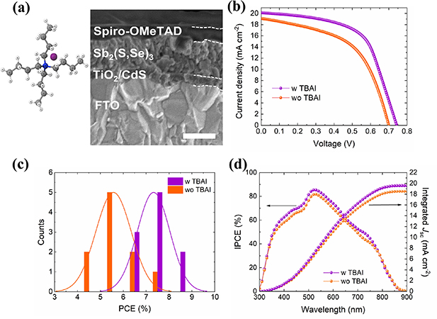
Figure 1. (a) Cross-sectional FESEM image of w TBAI device, including the chemical structure TBAI. Inset bar: 200 nm. (b) J–V curves of the champion w TBAI and wo TBAI devices, (c) histogram of the PCE distribution of ten individual devices. (d) IPCE spectra and integrated photocurrent density value over the entire IPCE spectra for w TBAI and wo TBAI solar cells.
Download figure:
Standard image High-resolution imageTo gain an understanding of the influence of TBAI addition on the photovoltaic performance, morphological and structural properties of the as-fabricated Sb2(S,Se)3 films were investigated. It is worth nothing that all the Sb2(S,Se)3 films evaluated were thermally treated to promote their crystallization, as indicated in the experimental section. Figures 2(a) and (c) display the top-view FESEM images of the Sb2(S,Se)3 samples grown without and with TBAI addition. It is observable that there are no significant changes in spherical-shaped grains. However, the film without TBAI exhibits broader particle distribution (figure S3) and larger number of surface cracks than those with TBAI, giving a total crack length of ∼24.6 and ∼10.3 μm, respectively. The crack length was determined from the processed SEM images, as described in the experimental section. AFM measurements were also used to further explore the surface morphology (figures 2(b) and (d)). The AFM images confirm the results obtained by FESEM. From the profile of the cross-section (inset) obtained along the dashed line in figure 2(b), the crack size is 124 nm wide and 31 nm depth for the film without TBAI. In addition, the surface roughness is reduced from 39.6 nm to 31.3 nm. The improved surface morphology and/or film quality is manifested in a larger shunt resistance (Rsh) in the w TBAI device. The values of Rsh were obtained from the J–V curves of figure 1(b), where the lower slope of the w TBAI device at potential close to zero can be related to a larger Rsh, i.e., 163 Ω cm−2 for wo TBAI and 384 Ω cm−2 for w TBAI.
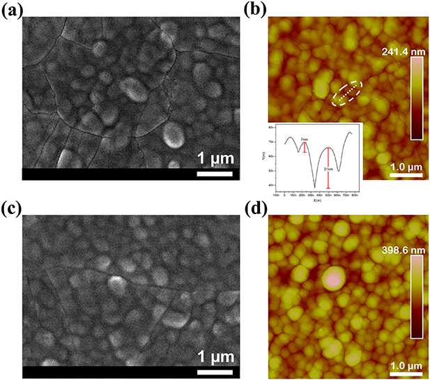
Figure 2. Top-view FESEM images and AFM images of the Sb2(S,Se)3 layer (a), (b) pristine, and (c), (d) with TBAI. The inset in figure (b) shows the depth profile of the AFM image obtained along the dashed line.
Download figure:
Standard image High-resolution imageThe XRD patterns of the Sb2(S,Se)3 films grown without and with TBAI are shown in figure S4(a). Both patterns exhibit nearly similar diffraction peaks without any additional impurity or new secondary phase. In the enlarged view of the XRD patterns in different 2θ ranges (figure 3(a)), the corresponding diffraction peak positions are between the standard PDF cards (PDF#42-1393) and (PDF#15-0861) of the binary antimony compounds, Sb2S3 and Sb2Se3, respectively. This indicates that both films exhibit the characteristic stibnite crystal structure. Compared with the pristine Sb2(S,Se)3 samples, the diffraction peaks of the film with TBAI are slightly shifted to lower angles and the relative intensities of the (211) and (221) planes decrease. Quantitatively, this trend is confirmed in the calculated texture coefficients of the (211) and (221) planes with TBAI, reducing its value by 16 and 13% (figure S4(b)). Apparently, after adding TBAI to the hydrothermal precursor solution benefits the growth of the (hk0) planes, promoting film growth parallel to the substrate, which has been related to a flat surface morphology [11]. It could also contribute to Se enrichment explaining the shift to lower diffraction angles [28]. Here, it is important to mention that the incorporation of TBAI into the crystal lattice can also alter the interplanar spacing, but it is unlikely that it remains as a molecule due to the crystallization thermal treatment of the Sb2(S,Se)3 film. XPS and Raman spectroscopy measurements were performed to assure the absence of TBAI in the Sb2(S,Se)3 surface. Figure 3(b) shows the high-resolution Sb 3d spectra of both Sb2(S,Se)3 samples. The XPS peaks of Sb 3d5/2 and 3d3/2 in the films without TBAI are centered at binding energies of 529.5 and 538.3 eV, respectively [28]. Remarkably, the characteristic Sb peaks of the Sb2(S,Se)3 grown in the presence of TBAI are also accompanied by slight shift towards lower binding energy, suggesting an effect of TBAI on the constituent elements of the Sb2(S,Se)3 surface. Figure S5(a) shows that this shift is also observed in the characteristic peaks of Se and S, which has been ascribed to the substitution of S with Se due to the electronegativity difference between the two atoms [15]. The ratio analysis of ISe/(ISe + IS) obtained by calculating the integrated area under Se and S peaks, i.e., Ise and IS, respectively, exhibits a significant increase from 0.19 (without TBAI) to 0.33 (with TBAI). Nevertheless, there are no additional XPS signals attributable to the incorporation of TBAI into the crystal lattice (figure S5(b)). In addition, the Raman spectra further proved the Se enrichment of the Sb2(S,Se)3 layers (figure 3(c)). The peak at around 216 cm−1 corresponds to the Sb–Se complex vibration, whereas the peaks at 280 and 314 cm−1 are ascribed to Sb–S vibration [18, 29]. For comparison, figure 3(c) also includes the typical Raman peak of tetrabutylammonium cations at 261 cm−1 obtained from TBAI precursor powder [30]. Similar to XRD and XPS results, there is no clear evidence of Raman peaks corresponding to the presence of TBAI in the thermally treated Sb2(S,Se)3 film, whereas in the as-deposited Sb2(S,Se)3 film before annealing shows the main peak of TBAI (figure S6). In figure 3(c), there is not a noticeable shift after adding TBAI as that observed in XRD and XPS, which can be due to an insufficient difference between the Se concentration of both samples to cause significant changes in vibrations. However, the relative intensity ratio of ISb-Se/ISb-S slightly increases from 0.31 to 0.45 with the presence of TBAI in the hydrothermal precursor solution, suggesting the Se enrichment of the Sb2(S,Se)3 film. EDS analysis was carried out to identify the atomic content ratios of Se/(Se + S) in the pristine film and with TBAI, as presented in table S2. It is found that after adding TBAI the atomic ratio increases from 0.17 to 0.21, which agrees well with the results obtained.
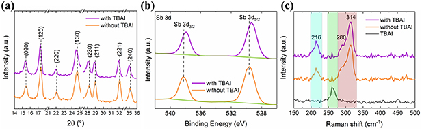
Figure 3. (a) XRD patterns, and (b) Sb 3d XPS profile of the Sb2(S,Se)3 samples without and with TBAI. (c) Raman spectra of both films including that of TBAI powder for comparison. The Raman peaks related to TBAI, Sb-Se, and Sb-S vibrations are highlighted in green, blue, and red, respectively.
Download figure:
Standard image High-resolution imageThe absorption spectra were used to examine the optical properties of both synthesized Sb2(S,Se)3 layers. As shown in figure 4(a), a negligible difference is found over the entire absorption curves of both films, although the absorption band edge is slightly varied. Thus, the optical band gap values were estimated by Tauc plot method (inset of figure 4(a)), being 1.57 and 1.6 eV for films with and without TBAI, respectively. These values are in agreement with those reported previously [31]. To evaluate the impact of adding TBAI on the electronic properties of the Sb2(S,Se)3 films, the work function (WF) was obtained by measuring the contact potential difference (CPD) in a Kelvin system. Briefly, the WF of the films is calculated by the equation [9]: CPD = (WFT−WFS)/e, where WFT and WFS represent the work functions of the gold probe and sample, respectively. Figure 4(b) shows that the average WF of the Sb2(S,Se)3 film decreases after adding TBAI from 4.88 to 4.79 eV, increasing its n-type character. A similar trend in optoelectronic properties has been previously reported as the atomic ratio of Se/(Se + S) increases, which results in a higher carrier concentration [5, 32].
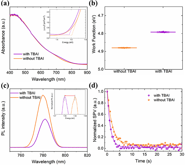
Figure 4. (a) Absorption spectra, (b) work function, (c) photoluminescence, and (d) surface photovoltage (SPV) decays of the Sb2(S,Se)3 films with and without TBAI. The inset of (a) shows the Tauc plot, whereas the inset of (c) shows a zoom of the normalized PL spectra.
Download figure:
Standard image High-resolution imageFigure 4(c) shows the steady-state photoluminescence (PL) spectra of the both Sb2(S,Se)3 samples. It is observed that the film with TBAI exhibits a lower PL intensity peak than that of pristine film, indicating a PL quenching after adding TBAI. This phenomenon suggests the efficient photogenerated electron charge transfer and transport within the Sb2(S,Se)3 film. Furthermore, the red shift of the PL emission peak at the same excitation wavelength (inset of figure 4(c)) is in accordance with the absorbance measurements. To obtain further insight into the charge-carrier dynamics, transient SPV study was carried out using the CPD under dark and superband gap illumination. The experimental SPV decays and their corresponding fits by using a bi-exponential model are shown in figure 4(d). According to this model, the recombination of the photogenerated free carriers in the Sb2(S,Se)3 bulk, along with at the surface/interface contribute to the two components [26]. The overall fit shows an excellent agreement with the experimental data. Compared with the pristine sample, the film with TBAI exhibits a faster SPV decay of the free electrons, indicating a reduction of the trap density. This reduction is consistent with previous works using ionic liquid in perovskite films [33, 34], who have suggested that a more n-type film improves the optoelectronic properties due to a reduction in the availability of electron traps.
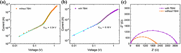
The SCLC analysis was used to investigate the consequence of the introduction of TBAI on the trap density (Nd) in both films. Thus, electron-only devices were assembled and measured the J–V characteristics under dark conditions (figures 5(a) and (b)). The linear relationship at low bias in the logarithmic J–V curves indicates an ohmic contact. Subsequently, the current rapidly increases with increasing the applied bias, indicating a transition to the trap-filled regime in which all available electron trap state are filled [35]. The transition voltage is defined as the trap-filling limit voltage (VTFL), and the Nd is determined by:  , where
  0 and r
are vacuum permittivity and the relative dielectric constant of the Sb2(S,Se)3, respectively; and L is the Sb2(S,Se)3 thickness. The film without TBAI reveals a trap density of 8.22 × 1015 cm−3, whereas that with TBAI shows a lower density of 6.17 × 1015 cm−3. The reduction of trap density demonstrates that an optimal concentration of TBAI into the precursor solution can effectively passivate the Sb2(S,Se)3 film defects, limiting the undesired nonradiative recombination. This observation is in agreement with the improved photovoltaic performance due to the enhanced transport and charge carrier within the Sb2(S,Se)3 films. EIS measurements reveal the beneficial influence of adding TBAI on the recombination phenomena of solar cells. Figure 5(c) depicts the Nyquist plots of the wo TBAI and w TBAI devices under dark conditions. The values of the recombination resistance (Rrec) and series resistance (Rs) can be extracted by fitting the Nyquist curves according to an equivalent electrical circuit [36]. The device with TBAI gives rise to a smaller Rs value than that of pristine device from 15.4 to 12.3 Ω, which is consistent with the above increased FF and Jsc. On the other hand, after adding TBAI the Rrec is significantly decreased about half of that of without TBAI. These findings indicate the successful suppression of carrier recombination, which contributes to maximize the Voc and PCE of the solar cells with TBAI.
0 and r
are vacuum permittivity and the relative dielectric constant of the Sb2(S,Se)3, respectively; and L is the Sb2(S,Se)3 thickness. The film without TBAI reveals a trap density of 8.22 × 1015 cm−3, whereas that with TBAI shows a lower density of 6.17 × 1015 cm−3. The reduction of trap density demonstrates that an optimal concentration of TBAI into the precursor solution can effectively passivate the Sb2(S,Se)3 film defects, limiting the undesired nonradiative recombination. This observation is in agreement with the improved photovoltaic performance due to the enhanced transport and charge carrier within the Sb2(S,Se)3 films. EIS measurements reveal the beneficial influence of adding TBAI on the recombination phenomena of solar cells. Figure 5(c) depicts the Nyquist plots of the wo TBAI and w TBAI devices under dark conditions. The values of the recombination resistance (Rrec) and series resistance (Rs) can be extracted by fitting the Nyquist curves according to an equivalent electrical circuit [36]. The device with TBAI gives rise to a smaller Rs value than that of pristine device from 15.4 to 12.3 Ω, which is consistent with the above increased FF and Jsc. On the other hand, after adding TBAI the Rrec is significantly decreased about half of that of without TBAI. These findings indicate the successful suppression of carrier recombination, which contributes to maximize the Voc and PCE of the solar cells with TBAI.
Figure 5. J–V characteristics of the electron-only devices assembled (a) without and (b) with TBAI under dark conditions. (c) Nyquist plots of both devices close to Voc.
Download figure:
Standard image High-resolution image
The long-term stability of the wo TBAI and w TBAI devices were tested in air at 25 °C and 61% humidity. It is important to note that these devices were stored without any encapsulation prior to the test. Figure S7 demonstrates that the w TBAI remains at about 91% PCE, whereas the wo TBAI maintained 83% PCE. Moreover, since the enhancement of surface hydrophobicity could improve the device stability, water contact angle measurements were also determined (inset of figure S7). The findings indicate that the w TBAI device has a more hydrophobic absorber film than wo TBAI. It is possible that the compositional change, i.e., Se enrichment, brought out by the presence of the additive in the hydrothermal precursor solution could be responsible for the changes in film hydrophobicity, which is outside of the scope of this work.
Although the best performing PCE of 8.87% obtained with our champion device is still lower than that record PCE of 10.7% [6], the main advantages of this strategy are its simplicity and low cost due to it does not require a post-hydrothermal process, reducing time and energy consumption.
4. Conclusions
In conclusion, we provide a facile additive strategy by incorporating a proper amount of TBAI into the precursor solution, leading to improved antimony selenosulfide solar cells performance. By adding TBAI, the Sb2(S,Se)3 film not only reduces the surface roughness and cracks, but also suppresses the formation of defects, improving the optoelectronic properties. The composition changes brought out by TBAI causes a shift in the Sb2(S,Se)3 work function toward higher energies increasing the n-type nature of the film. Further analysis demonstrates that the carrier recombination and the electron trap density were reduced in the devices based on Sb2(S,Se)3 film formed under the presence of TBAI. The optimal device with 0.62 mol% TBAI yields a champion PCE of 8.87%. Moreover, the PCE retains 91% of its initial value after 60 d of storage without encapsulation. This method provides a valuable strategy to reduce the presence of undesirable drawbacks in the antimony selenosulfide solar cells.
Acknowledgments
This work was performed with financial support of PAPIIT-UNAM (IN111722). R A Miranda-Gamboa and M A Millán-Franco acknowledge the PhD fellowships by CONACYT-México. The authors also thank the IER technicians: J Campos, E Barrios-Salgado, R Morán Elvira, M L Ramón, and G Casarrubias-Segura for their support.
Data availability statement
The data cannot be made publicly available upon publication because no suitable repository exists for hosting data in this field of study. The data that support the findings of this study are available upon reasonable request from the authors.
Conflict of interest
The authors have no conflicts to disclose.
Supplementary data (2.7 MB PDF)