
Abstract
We report on scalable heterointegration of superconducting electrodes and epitaxial semiconductor quantum dots (QDs) on strong piezoelectric and optically nonlinear lithium niobate. The implemented processes combine the sputter-deposited thin film superconductor niobium nitride and III–V compound semiconductor membranes onto the host substrate. The superconducting thin film is employed as a zero-resistivity electrode material for a surface acoustic wave resonator with internal quality factors  representing a three-fold enhancement compared to identical devices with normal conducting electrodes. Superconducting operation of
  resonators is achieved to temperatures
  and electrical radio frequency powers
  . Heterogeneously integrated single QDs couple to the resonant phononic field of the surface acoustic wave resonator operated in the superconducting regime. Position and frequency selective coupling mediated by deformation potential coupling is validated using time-integrated and time-resolved optical spectroscopy. Furthermore, acoustoelectric charge state control is achieved in a modified device geometry harnessing large piezoelectric fields inside the resonator. The hybrid QD—surface acoustic wave resonator can be scaled to higher operation frequencies and smaller mode volumes for quantum phase modulation and transduction between photons and phonons via the QD. Finally, the employed materials allow for the realization of other types of optoelectronic devices, including superconducting single photon detectors and integrated photonic and phononic circuits.
Export citation and abstract BibTeX RIS

Original content from this work may be used under the terms of the Creative Commons Attribution 4.0 license. Any further distribution of this work must maintain attribution to the author(s) and the title of the work, journal citation and DOI.
1. Introduction
Lithium niobate (LiNbO3) is a key material in the interconnected fields of nonlinear optics and acoustics due to its strong optical nonlinearity (e.g.  ) and piezoelectricity (e.g.
  ) [1–3]. LiNbO3's strong electro- and acousto-optical effects can be harnessed in quantum integrated photonic circuits [4, 5]. This unique combination of properties renders LiNbO3 a versatile host to synergistically combine various nonlinear photonic elements. Despite these advantages, LiNbO3 does not host optical emitters, which are required for many photonics applications. To overcome this shortcoming, several approaches are the focus of current research, including doping with rare earth ions [6, 7], direct growth [8] or transfer of 2D semiconductors [9–11], as well as heterogeneous integration of epitaxial semiconductors [12, 13].
One such method for integrating LiNbO3 with optically active quantum emitters is with piezoelectrically generated surface acoustic waves (SAWs), which mechanically deform the host material and have an associated electric field in piezoelectric materials. SAWs are highly appealing because of their universal coupling to dissimilar quantum systems [3, 14]. SAW devices are fabricated in a planar manner using straightforward CMOS device processing techniques, which has enabled optomechanical transduction between solid-state quantum emitters [15–17], integrated photonic and phononic circuits [18–21], and many other demonstrations of SAW coupling to optically or electrically active quantum systems sensitive to strain or electric fields [22–26]. Another advantage of SAW devices is that they typically operate at gigahertz (GHz) frequencies, where they can be cooled to the phononic ground-state without active cooling protocols [14, 17].
For quantum applications, SAW devices have to be further improved by mitigating loss channels. These include Ohmic heating in conducting electrodes of finite electrical conductivity. To alleviate these losses, SAW devices can be fabricated using superconducting electrode materials. For example, aluminum (Al) electrodes have been employed in SAW resonators of high quality factors  [27–29] proving the feasibility of this strategy. However, superconducting operation of such devices is limited to temperatures below aluminum's critical temperature
  . Such low temperatures are not strictly necessary for quantum control schemes of optically active solid-state two-level systems like semiconductor quantum dots (QDs) or defect centers. These QDs exhibit low decoherence already at moderate temperatures
  K, which are accessible with conventional
  cryostats. This low decoherence was impressively demonstrated by the implementation of all-optical coherent control schemes [30, 31]. These experiments are conducted under significantly relaxed conditions, i.e. higher operation temperatures compared to superconducting Al quantum systems. Thus, materials with moderately high
  would mark a significant advantage for hybrid SAW-QD devices. An additional challenge for integrating single quantum emitters with hybrid phononic quantum technologies remains the enhancement of the interaction strength between QDs and SAW phonons [32–35] and at the same time mitigating the aforementioned losses due to Ohmic heating by employing superconducting electrodes. The first has motivated the development of hybrid systems consisting of strong piezoelectric SAW substrates with heterogeneously integrated III–V compound semiconductors [36–38]. Heterogeneously integrated SAW devices are an extremely active field of current research, and recently large-scale radio frequency acoustoelectric devices have been realized [39, 40] This versatile approach is naturally suited to realize hybrid QD-SAW devices with transferred epitaxially grown QD layers [12, 41, 42]. For the latter, nitride-based superconductors are a leading material platform in the moderate temperature range because these materials exhibit much higher critical temperatures compared to Al. For example, niobium nitride (NbN) exhibits its superconducting transition at
  and is a well established material for superconducting single-photon detectors (SSPDs) [43–47]. SSPDs made from NbN and related compounds have been successfully demonstrated on a variety of substrates, including the materials used in this work: LiNbO3 [48–51] and GaAs [52, 53]. NbN and NbTiN single-photon detectors on LiNbO3-on-insulator waveguides have been demonstrated with system detection efficiencies of 46
 and 27
 , respectively [50, 51].
Here, we report on a scalable two-stage heterointegration process of III–V epitaxial QD heterostructures and superconducting electrodes on LiNbO3. In this process we adopt the fabrication technologies for NbN SSPDs, epitaxial lift-off, and bonding of III–V heterostructures. The full functionality of the fabricated devices is validated by verifying and quantifying two key performance metrics: (i) the superconducting transition of the electrodes and (ii) the optomechanical and acoustoelectric control of the QDs and simultaneous superconducting operation of the SAW electrodes.
The remainder of this article is structured in five sections. Sections 2 and 3 introduce the sample design and experimental techniques employed, respectively. Section 4 validates the electrical performance and superconducting operation. Section 5 reports on three different experimental approaches proving piezo-optomechanical control of QDs in our device. Section 6 summarizes the key findings and gives an outlook on the prospects of our approach and its future applications.
2. Sample design and fabrication
We implement our two-stage heterointegration on 128∘
Y-rotated LiNbO3, a common piezoelectric substrate for SAW resonator filters and delay lines with high electromechanical coupling  and phase velocity of
  at room temperature along the X-direction [54]. The prototype device is shown in figure 1(a). It is a one-port SAW-resonator aligned along the X-direction with NbN superconducting electrodes and an In(Ga)As QD heterostructure. In essence, two Bragg reflectors separated by a distance d form a SAW resonator with an effective cavity length
  . An interdigital transducer (IDT) is positioned in close proximity to one of the reflectors for SAW generation. This asymmetric configuration allows for heterointegration of large area semiconductor films. The electrodes of the Bragg reflectors and the IDT are made from NbN. The IDT electrodes are contacted by normal conducting pads. This configuration is adopted from our previous work [42] employing normal conducting electrodes which provides the reference for benchmarking the performance of the advanced design developed here. The process flow diagram for sample fabrication is schematically shown in figure 1(b). Steps (i)–(iii) are the first heterointegration stage in which the SAW component is realized. It follows a top-down route starting with a continuous thin film and, thus, is fully scalable to the wafer-scale. In step (i) a uniform 20 nm thick film of NbN is deposited directly on a 100 mm diameter LiNbO3 substrate using reactive DC magnetron sputtering. The NbN deposition parameters are as follows: 2 mT chamber pressure, 30 sccm argon and 4 sccm nitrogen gas flows, 250 V DC bias voltage. To generate high-quality superconducting NbN films with high
  , an RRR superconducting-grade Nb sputter target was used [55]. In step (ii) this film is subsequentially patterned using optical lithography and inductively coupled plasma (ICP) reactive ion etching with CF4 chemistry. The corresponding ICP etch parameters are the following: 0.4 Pa chamber pressure, 144 sccm CF4 and 9 sccm nitrogen gas flows, 850 W source power, 35 W bias power. The SAW resonators are finalized in step (iii) when pads composed of Ti (10 nm)/Au (90 nm) are defined by a lift-off process to contact the NbN electrodes of the IDT. The second heterointegration stage is step (iv) during which the semiconductor membrane is transferred onto the LiNbO3 using epitaxial lift-off and transfer [12, 56, 57]. For the devices we use the heterostructure shown in the right part of figure 1(a). It is grown by molecular beam epitaxy on a semi-insulating (001) GaAs substrate starting with a 100 nm thick AlAs sacrificial layer. The active part of the heterostructure consists of a 250 nm thick GaAs layer with a single layer of In(Ga)As at its center. This active part is removed from the growth substrate by selectively etching the AlAs sacrificial layer using hydrofluoric acid (HF) and then transferred onto the LiNbO3.
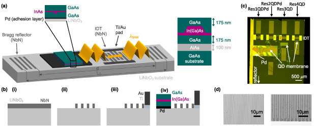
Figure 1. Device fabrication—(a) Schematic of the hybrid device. (b) Heterogeneous integration process flow: (i) NbN sputter deposition, (ii) optical lithography and etch, (iii) contact pad metallization lift-off, (iv) transfer of epitaxial III–V semiconductor heterostructure. (c) Optical microscope image of four devices of different cavity lengths with In(Ga)As QD heterostructure membranes heterointegrated. (d) Scanning electron microscope images of the reflectors (left) and the IDT (right).
Download figure:
Standard image High-resolution imageIn contrast to our previous work [12, 42], we study two types of devices. For the first type, shown in figure 1(a), analogous to our previous design, a 50 nm thick palladium (Pd) adhesion layer on top of a 5 nm thick titanium (Ti) layer defined via a lift-off process creates a strong and rigid metallurgic bond between LiNbO3 and the semiconductor. This layer also serves to shunt the piezoelectric fields, suppressing acoustoelectric charge carrier dynamics. For the second type, no Ti/Pd is used and consequently the interface between LiNbO3 and the semiconductor is no longer an equipotential plane. Thus, the piezoelectric potential induced by the SAW at the LiNbO3 surface extends into the semiconductor [58]. This allows the verification of piezo-optomechanical coupling comprising dynamic control of the QD energy levels and electric field driven ultrafast carrier dynamics [59–61] to regulate the charge state of the QD [62, 63]. The one-port SAW resonators were designed for a SAW wavelength  corresponding to a nominal SAW frequency of
  . These resonators had four different mirror spacings
  as shown in figure 1(c). The effective cavity length is given by
  , where d is the above spacing between the Bragg reflectors and
  is the mirror penetration depth for of a single Bragg reflector. For our electrode width
  and single-electrode reflectivity
  [42, 54, 64], we obtain
  . Figures 1(c) and (d) show optical and scanning electron microscope images of the final devices. Figure 1(c) shows that Res1QDPd and Res2QDPd contain QD membranes attached via a Pd adhesion layer, whereas the Pd layer is absent for Res3QD and Res4QD. Table 1 gives an overview of the different resonator designs (nominal SAW frequency f0, nominal SAW wavelength λ0, mirror spacing d, QD membrane, and Pd adhesion layer). Figure 1(d) shows high resolution images of the Bragg reflector (left) and the IDT (right) demonstrating successful pattern transfer into the NbN.
Table 1. Overview of the different resonator designs, where f0 nominal SAW frequency, λ0 is the SAW wavelength as defined lithographically, d is the mirror spacing defined lithographically, and the bottom two rows indicate the presence or absence of a QD membrane and a Pd adhesion layer.
| Device name | Res1 | Res1QDPd | Res2QDPd | Res2QD | Res3QD | Res4QD |
|---|---|---|---|---|---|---|
| f0 (MHz) | 300 | 400 | 400 | 400 | 400 | 400 |
| λ0 (µm) | 13.3 | 10.0 | 10.0 | 10.0 | 10.0 | 10.0 |
d

| 340 | 440 | 220 | 220 | 110 | 60 |
| d (µm) | 4522 | 4400 | 2200 | 2200 | 1100 | 600 |
| QD membrane | no | yes | yes | yes | yes | yes |
| Pd layer | no | yes | yes | no | no | no |
3. Characterization techniques
The sample was mounted on a custom-made carrier and wire-bonded. All experiments were conducted with the sample loaded into a variable temperature closed-cycle optical cryostat equipped with radio frequency (rf) signal lines. For rf characterization a vector network analyzer (VNA) was used to determine the S11 scattering parameter at different applied rf power levels  . The piezo-optomechanical response of single QDs was characterized by a combination of time-integrated and time-resolved photoluminescence (PL) spectroscopy [16]. Here, electrical excitation of the SAW resonator was performed using an rf signal generator. A directional bridge was used to analyze the reflected electrical power using an oscilloscope online during the optical experiment to ensure consistency between the optical and rf electrical data [42]. In the experiments presented here, optical excitation was performed using a continuous wave
  diode laser focused to a diffraction limited spot with a diameter of
  by a
by a  microscope objective with a focal length of 2.89 mm. A moderate optical pumping density
  ensured preferential generation of single exciton species with no noticeable signatures of biexcitons. The emission of the QDs was collected by the same objective and dispersed in a 0.7 m grating monochromator. Time-integrated multi-channel detection was performed using a cooled CCD detector. For single-channel time-resolved detection, the detection wavelength was scanned and the signal was recorded by a single photon avalanche diode (SPAD) with time resolution
  ps. The electrical pulses of the SPAD were recorded with time correlation electronics referenced to the electrical signal applied to the IDT [21, 65].
4. Electrical characterization
We first validate the electrical operation of our device in the superconducting regime of NbN and determine the accessible ranges of the main operation parameters, the sample temperature, T, and the rf electrical power,  , applied to the IDT. Figure 2 shows a comprehensive set of data and their analysis for resonator Res1 before transfer of the QD heterostructure. The nominal design frequency was
  with a nominal mirror distance of
  with
with  . We begin with applying a constant low rf power
  and measure the S11 scattering parameter as a function of the applied electrical frequency for different values of the sample temperature in the cryostat. These data are plotted in figure 2(a) with T increasing from the bottom to top spectrum. The spectrum recorded at the base temperature
  shows the expected resonator response with clearly resolved minima in the reflected rf power at the resonance frequencies of the cavity modes (vertical dashed lines). The measured free spectral range
  corresponds to an effective resonator length
  , in good agreement with the nominal lithographically defined cavity length
  . Second, the measured S11 can be fitted using
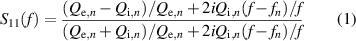
with  and
and  being the internal and external Q-factors of mode n at frequency fn
[64]. At base temperature, we obtain values ranging between
being the internal and external Q-factors of mode n at frequency fn
[64]. At base temperature, we obtain values ranging between  , indicating a three-fold improvement compared to identical resonator devices equipped with normal conducting Ti/Al electrodes [42].
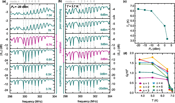
Figure 2. Electrical characterization—(a) Scattering parameter S11 of a  SAW resonator at
  with temperature T increasing from bottom to top and (b) at T = 3.7
  with
with  increasing from bottom to top. (c) Phase diagram in the
  -T parameter space indicating the phase boundary from the superconducting to normal conducting state. (d) Internal quality factor Qi
of the phononic modes as a function of T.
-T parameter space indicating the phase boundary from the superconducting to normal conducting state. (d) Internal quality factor Qi
of the phononic modes as a function of T.
Download figure:
Standard image High-resolution imageAs T increases, we observe the transition from superconductivity to normal conductivity at  (purple spectrum). For temperatures above
  , we observe a characteristic change of the spectrum with the emergence of peaks (instead of dips) that are shifted in frequency compared to the modes in the superconducting state (dashed lines). This behavior is expected for loss-dominated resonators, which is the case for NbN thin films above
  . Its conductivity is at least one order of magnitude lower than commonly used normal conducting metals like aluminum [54, 66, 67]. In figure 2(b) we show analogous S11 spectra with the temperature held constant at
  and the electrical power applied to the IDT increasing from the bottom to the top. As
  increases from
  , we observe a clear change of the spectrum at
  (purple). This change is markedly different to the abrupt change in figure 2(a) between
  and
and  . Here, the dips at the resonator mode frequencies broaden continuously and evolve in a spectrum similar to the normal conducting state at the highest power level
  . This continuous broadening cannot be explained by a change of the global sample temperature, but instead indicates a local breakdown of superconductivity in a subset of the electrodes. Since the cavity mode frequencies (vertical grey lines) remain constant, we conclude that superconductivity is initially preserved in the Bragg mirrors' electrodes. Breakdown occurs locally in the IDT electrodes, where the driving rf electrical signals drives a current. The corresponding local increase of the current density above the critical value breaks superconductivity. This occurs first at the cavity resonance where the highest current densities are reached. With increasing
  , the critical current density is reached off-resonance giving rise to the observed apparent broadening. At the highest
  , superconductivity breaks down over the entire range of frequencies. Ohmic heating in this normal conducting state raises the global sample temperature above
  , retaining a spectrum similar to that observed in figure 2(a).
To further corroborate this interpretation we analyze the observed  as a function of
  , plotted in figure 2(a). These data show that an increase of
  leads to a decrease of the measured
  . At this point we bear in mind that an increase of
  corresponds to an increase of the current density. Thus the data in figure 2(a) corresponds to an effective phase boundary of a superconductor in the current-temperature parameter space. Finally, we analyze
  as a function of T obtained from a best fit of equation (1) to the data in figure 2(a). The obtained values for modes
  are plotted for temperatures
  in figure 2(d). The data clearly show that high
  is in fact preserved for all modes up to
  when superconductivity breaks down. To summarize, the performed electrical characterization proves superconducting operation with high internal
  . The derived effective phase boundary defines the parameter space for the operation of our device. For all experiments shown in the remainder of this article, the effective phase boundary was first pinpointed to ensure superconducting operation in the optical experiments.
5. Piezo-optomechanical characterization
In the second phase of our characterization, we investigate the piezo-optomechanical interaction between the SAW resonator and the QDs in the heterointegrated device. We probe the optomechanical coupling between single QDs and phononic modes by measuring the optical emission as a function of the applied rf parameters. In all these experiments, the electrodes are in the superconducting state. Thus we validate combined superconducting operation and SAW control of single QDs. In the following, the design frequency of the investigated devices is  . In sections 5.1 and 5.2, we use the Res2QDPd resonator with the QD heterostructure transferred onto a Pd adhesion layer in its center. The Pd shunts the electric field induced by the SAW [12, 41]. Accordingly, Stark-effect modulation, which becomes dominant at high SAW amplitudes [58] and acoustoelectric charge state regulation [62, 68] are effectively suppressed and can be neglected in the following. In section 5.3 we use a Res2QD resonator where a QD heterostructure is directly transferred onto the LiNbO3 without a Pd adhesion layer. In this case, the piezoelectric fields can induce spatio-temporal carrier dynamics and thus, regulate the charge state of the QD.
5.1. Time-integrated optomechanical characterization
We first measure the optomechanical response of a single QD by time and phase averaged PL spectroscopy. As schematically shown in figure 3(a), the detected line shape is a time-average of the sinusoidally modulated Lorentzian QD emission line [58, 69] given by
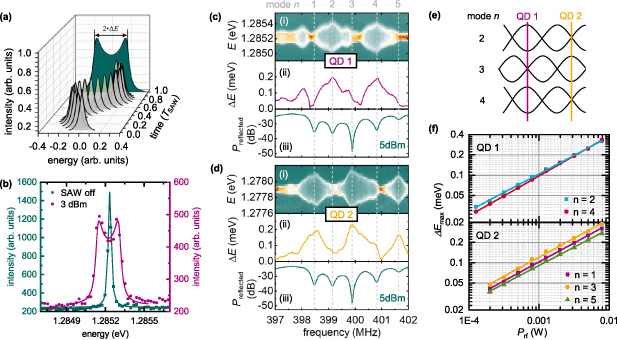
Figure 3. Piezo-optomechanical characterization—(a) Schematic of dynamic modulation of Lorentzian emission line giving rise to the time-integrated spectrum given by (2). (b) Emission line of a single QD (data points) without a SAW applied (green) and with a SAW applied (purple) with best fits of equation (2) (solid lines). (c) and (d) PL spectrum (i), extracted  (ii) and reflected electrical rf power (iii) recorded from QD 1 and QD 2, respectively. (e) Schematic of site-selective coupling of QD 1 and QD 2. (f)
  for different phononic modes as function of
  of QD 1 (top) and QD 2 (bottom).
Download figure:
Standard image High-resolution image
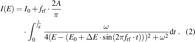
In this expression, I0 denotes a time-independent intensity offset, E0 the center energy, A the amplitude, ω the width of the Lorentzian emission peak, and  the optomechanical modulation amplitude. Figure 3(a) schematically shows the sinusoidal modulation of the Lorentzian emission line of a single QD (gray) and the resulting time-integrated emission spectrum (green) with its optomechanical tuning amplitude labeled as
  . Figure 3(b) shows the measured time-integrated emission spectra of a exemplary QD (data points) and a best fit of equation (2) (solid line). Without a SAW applied (green), the expected Lorentzian line is faithfully detected. When strained by a SAW (
 dBm,
dBm,  MHz, purple), the characteristic lineshape given by equation (2) is observed.
Next, we confirm the optomechanical coupling of QDs to the SAW resonator modes. To this end, we begin by applying  dBm to the IDT, at which the resonator was verified to be in the superconducting state. We then scan
  from 397 to 402 MHz. We select two QDs, QD 1 and QD 2, which are separated by
  along the axis of the resonator. The results of the performed characterization experiments are shown for QD 1 and QD 2 in figures 3(c) and (d), respectively. The upper panels (i) show the time-integrated PL intensity as a function of electrical
  (horizontal axes) applied to the IDT and photon energy (vertical axes). The lower panels (iii) show the simultaneously recorded reflected rf power to identify the involved SAW modes fn
of mode index (n) of the hybrid SAW resonator. These are labeled and marked by the vertical dashed lines. The center panels (ii) show
(horizontal axes) applied to the IDT and photon energy (vertical axes). The lower panels (iii) show the simultaneously recorded reflected rf power to identify the involved SAW modes fn
of mode index (n) of the hybrid SAW resonator. These are labeled and marked by the vertical dashed lines. The center panels (ii) show  of the two QDs extracted from the experimental data by fitting equation (2). These data clearly prove the anticipated site and frequency selective coupling of the embedded QDs and the phononic modes. QD 1 in figure 3(c) shows strong optomechanical response
  and, thus, strong optomechanical coupling when
  is in resonance with an even index mode
  . Conversely, this coupling is suppressed for odd index models
  . The optomechanical coupling is inverted for QD 2 in figure 3(d), which exhibits strong and weak coupling for
  and
and  , respectively. These observations are in agreement with the QD 1 being at the antinodes of the
  modes and QD 2 being at those of the
  modes as shown schematically in figure 3(e) [42].
In a third step, we study the dependence of the optomechanical modulation  on the applied rf power. We increase
  from
from  in steps of
  to
to  and record the resulting
  of QD 1 and QD 2. In this range of
  , the device is in the superconducting state, which was confirmed by the simultaneously measured electrical power reflected from the device. This measured range is
  larger than that of the
  device shown in figure 2. The extracted
  of QD 1 and QD 2 are plotted as a function of
  in the upper and lower panel of figure 3(f), respectively. These data are presented for all modes to which the respective QDs couple. Moreover, the data is plotted in double-logarithmic representation to identify the power law dependence
  and the underlying coupling mechanism. QD 1 exhibits a power law dependence with an average slope
  and QD 2 with
  . The amplitude of the SAW,
  , and
, and  . Hence, a slope of
  is a characteristic fingerprint for deformation potential coupling being the dominant mechanism [16]. We note that the small increase compared to the ideal value of m = 0.5 may arise from a weak nonlinearity as observed for similar hybrid devices with normal conducting electrodes [42]. Moreover, the extracted slope excludes Stark effect modulation for which m = 1 is expected [58].
5.2. Time-resolved optomechanical characterization
Next, we perform time-correlated single-photon counting to resolve the SAW-driven dynamics of QD 3 directly in the time domain. This type of characterization allows direct observation of the temporal shift of the QD emission line, which was not addressed in our previous work on hybrid QD-SAW resonators with normal conducting electrodes [42]. In the following,  dBm is fixed. Before conducting these time-resolved measurements, we study the time-integrated emission of QD 3 as in the previous section to determine the position of the selected QD in the SAW cavity field. Figure 4(a) shows the time-integrated emission spectrum of QD 3 (top panel) and the simultaneously measured reflected rf power (bottom panel) as a function of
  . From these data we conclude that QD 3 couples strongly to odd modes and only weakly to even modes. The derived relative position of QD 3 within the SAW cavity field is shown schematically as an inset of figure 4(a). In addition and in agreement with the data shown in figure 3 and [42], a pronounced optical response can be found in the frequency range between the n = 2 and n = 3 modes. The time-resolved analysis of the dynamically strained QD 3 is performed for three characteristic frequencies
  marked by different colored lines in figure 4(a).
  MHz corresponds to the resonance of mode n = 1.
  MHz and
  MHz are chosen in between the n = 2/n = 3 and n = 3/n = 4 modes, respectively. At these frequencies, QD 3 shows strong (f23) and weak (f34) modulations. The top panels of figure 4(b) present plots of the temporal modulation of the QD emission line at the three selected frequencies in false color representation. In all three cases, a clear sinusoidal modulation is observed in the time domain. Furthermore, the period of these modulations correspond to that set by the applied rf. The bottom panels of figure 4(b) show the peak positions (black) as a function of time extracted from these data by best fits of a Lorentzian line for each time stamp. By fitting the obtained data with a sine function (solid orange, blue, and purple lines) we extract modulation frequencies of the QD
  ,
,  , and
, and  . These values agree well with the electrical rf. Thus, these data prove that in this sample the QD is predominantly modulated at the SAW excitation frequency, regardless of its location in the phononic mode spectrum. These findings furthermore clearly indicate that no dominant wave mixing processes occur in the SAW resonator and that the dominant coupling mechanism is deformation potential coupling.

Figure 4. Time-resolved dynamic modulation—(a) Time integrated PL spectrum of QD 3 and reflected rf power. The inset shows the position of QD with respect to the n = 2 and n = 3 modes. (b) Time-dependent PL spectra (top) for three selected  marked in (a) and extracted spectral modulations (bottom).
Download figure:
Standard image High-resolution image5.3. Acoustoelectric charge state control
Finally, we demonstrate acoustoelectric control of the charge states of single QDs on our hybrid platform. To this end, we study resonator Res2QD with a nominal SAW frequency of  with a mirror spacing d = 220 λ0 and a QD heterostructure directly transferred onto the LiNbO3 without a Pd adhesion layer. Again, the design frequency is
  as confirmed by the SAW mode spectrum plotted in the lower panel of figure 5(a). The upper panel of figure 5(a) shows the emission spectrum of two QDs, QD 4 and QD 5 (plotted in false-color representation as a function of
  ). These data are recorded at relatively low rf power of
  at which strain coupling is dominant [58, 63]. Thus, both emission lines QD 4 at
  and QD 5 at
  show the expected broadening when
  is tuned into resonance with modes of odd (
 ) index, while no significant coupling is observed for modes of even index (
 ). Thus, we can conclude that both QDs are at the antinodes (nodes) of the strain field of odd (even) index modes. This observation proves mode-selective strain coupling of the QD to the SAW even with a relatively weak van der Waals bond between the semiconductor and LiNbO3 substrate, compared to the rigid metallurgical bond for the devices with the Pd adhesion layer. Next, we increase the rf power to
  and plot the recorded emission spectra in the same range of photon energies and
  in false-color representation in the center panel of figure 5(a). These data exhibit a completely different behavior than those of samples with a Pd adhesion layer (cf figures 3, 4 and [12, 42]) arising from the combination of strain tuning and acoustoelectrically driven carrier dynamics by the SAW. In this device without the Pd adhesion layer, no highly-conductive metal shortens the piezoelectric fields induced by the SAW on the LiNbO3–GaAs interface. Thus, the electric field extends into the semiconductor. This field efficiently ionizes the photogenerated excitons and induces spatio-temporal charge carrier dynamics (STCDs) [59, 60, 70]. The induced dynamics regulate the charge state of the QDs on timescales of the SAW and lead to correlated suppression and emergence of different emission lines [62, 68]. We note that in contrast to other previous work, these dynamics are observed within a SAW resonator, and no freely propagating SAWs were employed.

Figure 5. Acoustoelectric charge state regulation—(a) PL spectra as function of  at
at  (top) and
  (center) showing the emission of QD 4 and QD 5 and simultaneously measured reflected rf power (bottom). (b) Schematic SAW-induced bandstructure modulation in the device and the resulting acoustoelectric electron (purple) and hole (green) dynamics for one full acoustic cycle. Dashed lines mark the position of QD 4 when even and odd index modes are excited.
Download figure:
Standard image High-resolution image
In the following analysis, we focus on QD 4 for which different emission lines can be clearly identified. In order to understand the experimental findings, we have to consider that our device is a SAW resonator in contrast to devices with propagating SAWs studied previously in literature. In our resonator, the nodes of the phononic modes' standing wave pattern are stationary. To understand the experimental findings, we have to consider the time-dependent strain and electric field at the position of QD 4 for a given mode index n. As shown above, QD 4 is located at the antinodes of odd index ( ) modes and at nodes of even index (
 ) modes. For X-propagating SAWs on 128∘
Y-rotated LiNbO3, the volume dilatation inducing the optomechanical modulation and the electric potential are in phase and simultaneously tune the emission line and regulate the occupancy state. Figure 5(b) schematically depicts the dynamic evolution of the bandstructure modulation at four distinct times during the acoustic cycle. At t = 0, the amplitude of piezoelectric potential of the SAW is maximum. Thus, the corresponding sinusoidal modulation is superimposed giving rise to the well established type-II band-edge modulation [71]. At
) modes. For X-propagating SAWs on 128∘
Y-rotated LiNbO3, the volume dilatation inducing the optomechanical modulation and the electric potential are in phase and simultaneously tune the emission line and regulate the occupancy state. Figure 5(b) schematically depicts the dynamic evolution of the bandstructure modulation at four distinct times during the acoustic cycle. At t = 0, the amplitude of piezoelectric potential of the SAW is maximum. Thus, the corresponding sinusoidal modulation is superimposed giving rise to the well established type-II band-edge modulation [71]. At  , the situation is reversed and positions of maxima and minima are exchanged. At
  and
and  , destructive interference of the SAW fields occurs and leads to an unperturbed flat bandstructure. In these schematics, the vertical dashed lines indicate the position of QD 4 in this bandstructure when odd index (
 ) modes or even index (
 ) modes are excited.
For  , QD 4 is at the node of the electric potential modulation. Thus, the resulting gradient and hence amplitude of its electric field is maximum. This leads to an efficient dissociation of excitons and pronounced STCDs as shown in the schematics of figure 5(b). In the experimental data, we observe a strong suppression of the emission line observed for the weakly modulated case at
  and a new emission line at
  . This switching is a characteristic fingerprint of acoustically regulated carrier injection driven by STCDs. For
  , QD 4 is at the antinode of the electric potential modulation. Thus, the gradient and electric field vanishes and the STCDs are dominated by redistribution processes of electrons and holes from their unstable points (and position of the QD) to regions of maximum electric field. These processes are indicated in the schematics of figure 5(b) and are slow compared to field-driven drift. This leads to marked changes in the carrier injection dynamics into QD 4 which favors the preferential generation of different occupancy states and resulting emission lines for different n. For n = 1, the occupancy state corresponding to the
  line is preferentially generated, while for n = 3, that of the
  line. For n = 5, both lines are almost completely suppressed which points towards efficient carrier depletion at the position of the QD 4. When tuning
  , a characteristic and reproducible switching pattern is observed. This observation unambiguously proves that the direct coupling of QD heterostructure to the LiNbO3 substrate leads to pronounced STCDs and charge state regulation which can be efficiently suppressed by a thin metallic layer shunting the electric fields. Note that detailed modeling at the level possible for propagating SAWs [62, 63] is not possible for the devices studied here. As shown for the piezo-optomechanical response the complex mode pattern of our resonator comprises contributions of propagating and stationary waves. The observed switching hampers the faithful disentanglement of these contributions, which would be required to perform numerical simulations of the STCDs.
6. Conclusion
In summary, we developed and implemented a two-step heterointegration process of a hybrid SAW-resonator device comprising superconducting electrodes and an epitaxial semiconductor heterostructure on a LiNbO3 substrate. Our facile process can be scaled to the wafer-scale by building on recent breakthroughs in this field. Firstly, the here applied transfer of millimeter-sized and few 100 nm thick semiconductor heterostructure membranes can be realized at the wafer-scale through wafer bonding techniques [39, 40, 72]. Secondly, superconducting thin films are sputter-deposited and patterned in a subtractive process, which is in principle also directly scalable. We validated the functionality of the fabricated devices by characterizing the parameter space for superconducting operation of the SAW component. In these first experiments, we monitored the superconducting to normal conducting transition of the NbN electrodes as a function of temperature and applied electrical rf power. The achieved internal quality factor  marks a three-fold improvement to previously studied similar devices using normal conducting electrodes [42]. After transfer of the III–V semiconductor, we verified the combined superconducting operation of the SAW device and piezo-optomechanical control of the embedded QDs. In a series of experiments, mode-selective coupling of the QDs, time-modulation of the QD emission line, and acoustically regulated carrier injection are verified. The latter observation provides direct evidence of spectral tuning of the QD by dynamic strain and simultaneous acoustoelectric regulation of the QD's occupancy state for the first time in a SAW resonator.
Our two-step heterointegration opens directions for advanced piezo-optomechanical quantum devices. First, our superconducting SAW resonators are fabricated with the same processes used for NbN single-photon detectors [51], enabling future SAW devices to be integrated with SSPDs during a single fabrication step. Second, the performance of our resonators can be deliberately enhanced to small mode volume ( ), higher Q-factor, and high frequency (
 1 GHz) operation [73]. These devices then harness the large K2 of LiNbO3 and strong optomechanical coupling of III–V semiconductor QDs [32–34]. These may ultimately enable coherent optomechanical control in the sideband regime [35, 74]. Third, the process can be extended to additional heterointegration steps for example adding defect quantum emitters providing spin qubits serving as quantum memories [26, 75–77].
Acknowledgments
We gratefully acknowledge support via the UC Santa Barbara NSF Quantum Foundry funded via the Q-AMASE-i program under award DMR-1906325. This project was funded by the Deutsche Forschungsgemeinschaft (DFG, German Research Foundation)—465136867 and the Bavaria-California Technology Center BaCaTeC (Förderprojekt Nr. 8 [2020-1]). K M acknowledges financial support via the German Federal Ministry of Education and Research (BMBF) via the funding program Photonics Research Germany (Contract Number 13N14846). M L and J J F acknowledge funding by the Bavarian Hightech Agenda within the Munich Quantum Valley doctoral fellowship program. J J F and K M acknowledge financial support by the Deutsche Forschungsgemeinschaft (DFG, German Research Foundation) under Germany's Excellence Strategy-EXC-2111-390814868. We thank Hubert Riedl (WSI-TUM) for crystal growth.
Data availability statement
The raw data that support the findings of this study are openly available at the following URL/DOI: https://doi.org/10.5281/zenodo.8003086.