

Abstract
Emerging wide bandgap BAlN alloys have potential for improved III-nitride power devices, including high electron mobility transistors (HEMTs). Yet, few relevant studies have been carried out. In this work, we have investigated the use of the B0.14Al0.86N alloy as part or the entirety of the interlayer between the GaN buffer and the AlGaN barrier in the conventional GaN/AlGaN heterostructure. The numerical results show considerable improvement of the two-dimensional electron gas (2DEG) concentration with small 2DEG leakage into the ternary layer by replacing the conventional AlN interlayer by either the B0.14Al0.86N interlayer or the B0.14Al0.86N/AlN hybrid interlayer. Consequently, the transfer characteristics can be improved. The saturation current can be enhanced as well. For instance, the saturation currents for HEMTs with the 0.5 nm B0.14Al0.86N/0.5 nm AlN hybrid interlayer and the 1 nm B0.14Al0.86N interlayer are 5.8% and 2.2% higher than that for the AlN interlayer when VGS−Vth = +3 V.
Export citation and abstract BibTeX RIS

Original content from this work may be used under the terms of the Creative Commons Attribution 4.0 license. Any further distribution of this work must maintain attribution to the author(s) and the title of the work, journal citation and DOI.
1. Introduction
In the past decades, III-nitride semiconductors, especially AlGaN, InGaN, and GaN, have been widely employed for optical and electronic devices due to their superior properties, such as suitable bandgap, high saturation velocity, high breakdown field, and high chemical and thermal stability. Invented in 1993 based on the two-dimensional electron gas (2DEG) at the AlGaN/GaN heterointerface induced by the net polarization charge, the GaN-based high electron mobility transistor (HEMT) has attracted enormous research interest due to its vast high power and high speed applications [1]. Since then, substantial efforts have been made to improve the GaN-based HEMT performance [2]. Previously, there have been reports of the use of organic interlayers to regulate the charge transport in organic transistors [3–6], and the organic molecules could also be applied in GaN-based HEMTs to improve the transport properties [7]. In general, a higher Al content of the AlGaN barrier layer can induce larger net polarization charge at the AlGaN/GaN heterointerface, resulting in higher 2DEG concentration in the conventional AlGaN/GaN HEMT structure. However, the electron mobility can be compromised due to the scattering caused by the alloy disorder. Additionally, further increasing the Al content of the AlGaN barrier layer could degrade the interface quality due to the larger lattice mismatch between the AlGaN barrier layer and the GaN buffer layer [8].
To overcome the issues, the insertion of a thin (≤2 nm) AlN interlayer between the barrier layer and the GaN channel layer has been proposed and implemented, partly because the binary AlN does not cause alloy scattering. A thicker AlN interlayer is not feasible, as the AlN interlayer could relax due to the large lattice mismatch with the GaN buffer layer. Furthermore, the AlN interlayer can elevate the barrier height for the 2DEG due to its higher conduction band edge than that of the AlGaN barrier. Since the penetration of the electron wave function into a given barrier is in inverse proportion to the barrier height, the AlN interlayer could suppress the 2DEG leakage into the barrier, further suppressing the alloy scattering [9]. Moreover, the net polarization charge at the AlN/GaN heterointerface is greater than that of the AlGaN/GaN heterointerface, which induces a higher 2DEG concentration. Combining the three benefits, the AlN interlayer has been employed to minimize the alloy scattering and enhance the 2DEG concentration [10].
The wurtzite BAlN alloys with large bandgap have application potentials for III-nitride devices. Recently, meaningful progress has been made in studying epitaxy and the properties of BAlN thin films and heterojunctions. The growth of a highly reflective BxAl1-xN/AlN distributed Bragg reflector was conducted by metalorganic vapor phase epitaxy (MOVPE) [11]. The growth of five-period BxAl1-xN/AlN heterostructures with the boron content of 11% has been demonstrated [12], and researchers have performed the growth of single-crystalline BAlN layers with relatively high boron composition by MOVPE [13–15]. Moreover, the lattice constant and polarization properties of the BAlN alloys have been studied, in which large variations of those important quantities were found [16–18]. The net heterointerface polarization charges of the strained AlxGa1-xN/GaN (0 ≤ x ≤ 1) heterostructures on relaxed GaN are much smaller compared to those of the strained AlxGa1-xN/B0.14Al0.86N (0 ≤ x ≤ 1) heterostructures on relaxed GaN with similar Al composition x's of AlxGa1-xN. For instance, the absolute values of the net heterointerface polarization charges of the Al0.3Ga0.7N/GaN heterojunction is 0.0335 C m−2 [19]. In comparison, the absolute values of the net heterointerface polarization charges of the Al0.3Ga0.7N/B0.14Al0.86N and GaN/B0.14Al0.86N heterojunction are 0.1364 C m−2 and 0.1699 C m−2, which could offer significantly more band bending. Furthermore, the band alignments of the BAlN/(Al)GaN heterojunctions have been determined, showing an extremely large conduction band offset between BAlN and (Al)GaN due to the type-II nature, which is distinct from the type-I nature for the AlxGa1-xN/GaN (0 ≤ × ≤ 1) heterostructures [20, 21]. Despite the unique polarization and band offset properties, however, there have been few device research reports about the incorporation of the BAlN alloys in the technically-important HEMTs.
In this work, we propose to incorporate the BAlN alloy into the GaN HEMTs by leveraging its unique band alignment and polarization properties. Specifically, a thin BAlN layer is employed as the whole interlayer or as part of the interlayer in the conventional AlGaN/GaN-based HEMTs to provide considerably larger polarization charge at the heterointerface and thus 2DEG concentrations, while effectively suppressing the electron leakage into the AlGaN barrier layer through a larger conduction band offset than the conventional AlN interlayer.
2. Impact of interlayers on 2DEG characteristics
The simulation structures are constructed based on the conventional wurtzite III-polar GaN-based HEMT comprising a fully-relaxed GaN buffer layer, a 1 or 2 nm interlayer, and an Al0.3Ga0.7N barrier layer, shown in figure 1(a) [22–24]. For the interlayers, various designs under consideration include: 1 nm B0.14Al0.86N interlayer, 2 nm B0.14Al0.86N interlayer, 0.5 nm B0.14Al0.86N/0.5 nm AlN hybrid interlayer, 1 nm B0.14Al0.86N/1 nm AlN hybrid interlayer, 1 nm AlN interlayer, and 2 nm AlN interlayer, as shown in figures 1(b)–(e). It should be noted that for the structures without the interlayer, we increase the Al0.3Ga0.7N barrier thickness from 25 nm to 26 nm and 27 nm corresponding to the 1 and 2 nm Al0.3Ga0.7N interlayers, respectively, in order to keep the total thickness fixed for fair comparison. The B-content of 14% is chosen, i.e. the B0.14Al0.86N alloy, because its band alignment with (Al)GaN could be promising for the enhanced GaN-based HEMT and it has been realized epitaxially by our group. As shown by previous studies, sharp interfaces were observed for B0.14Al0.86N/Al0.7Ga0.3N and B0.14Al0.86N/GaN heterojunctions without boron diffusion, which have much larger thickness than our proposed 1 nm and 0.5 nm of the B0.14Al0.86N layers of the hybrid B0.14Al0.86N/AlN interlayers [20, 21]. The maximum thickness of the interlayer is limited at 2 nm as larger thicknesses could lead to lattice relaxation given the large lattice mismatch between the interlayer and the buffer layer, thus poorer material quality [25]. The entire HEMT structure is assumed to be fully strained to the GaN buffer layer. The B0.14Al0.86N/AlN heterojunction where AlN situates between B0.14Al0.86N and GaN is employed to minimize potential alloy scattering. The dielectric SiNx is applied for surface passivation. The length of the Schottky gate, the gate-to-source spacing, and the gate-to-drain spacing are set according to the typical values of the GaN-based HEMT shown in figure 1(a). The channel dimensions are the same for all the structures for fair comparison.
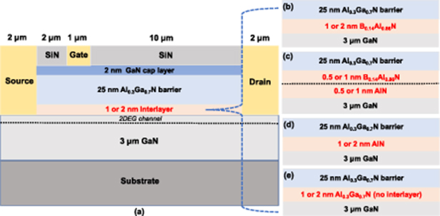
Figure 1. (a) Cross-sectional schematics of the HEMT structures with different interlayer configurations: (b) 1 or 2 nm B0.14Al0.86N, (c) 0.5 nm B0.14Al0.86N/0.5 nm AlN or 1 nm B0.14Al0.86N/1 nm AlN, (d) 1 or 2 nm AlN, (e) 1 or 2 nm Al0.3Ga0.7N (i.e. no interlayer).
Download figure:
Standard image High-resolution imageThe simulation employs APSYS developed by Crosslight Inc. [26]. The electrical properties of the structures are performed by solving Poisson's equation and the continuity equation. The transport model of electrons and holes including drift and diffusion are considered. The electron transport is based on the mobility models inside APSYS, which are the Caughey–Thomas model and modified transferred electron model for different electric filed conditions [27, 28]. The formation of the 2DEG amid the HEMT structures are mainly related to the heterointerface polarization difference and the band offset. The lattice constants, polarization parameters, and band offsets of the involved materials are from [16, 17, 20, 21], from which it can be deduced that the B0.14Al0.86N/GaN heterojunction exhibits a significantly larger conduction band offset and heterointerface polarization difference as compared to the conventional AlN/GaN and Al0.3Ga0.7N/GaN heterojunctions, potentially leading to much higher 2DEG concentration and less 2DEG leakage from the channel into the barrier.
The conduction band diagrams and the polarization-induced electron concentration of the HEMT structures with and without the 1 nm and 2 nm interlayers under zero bias are plotted in figures 2(a) and (d). Due to larger polarization sheet charge induced by B0.14Al0.86N, the conduction bands of the GaN buffer layer bend down the most below the Fermi level at the interlayer/buffer interface for the 1 nm and 2 nm B0.14Al0.86N interlayers om figures 2(a) and (c), respectively, followed by the hybrid interlayers and the AlN interlayers. The structures without the interlayers have the smallest conduction band bending. As the increased band bending below the Fermi level induces more electrons at the channel, the use of the B0.14Al0.86N interlayers leads to the highest concentration of electrons, followed by the hybrid interlayers, the AlN interlayers, and the structures without the interlayers are shown in figures 2(b) and (d).

Figure 2. (a) Band diagram and (b) electron concentration of the HEMT structures with and without the 1 nm interlayers. (c) Band diagram and (d) electron concentration of the HEMT structures with and without the 2 nm interlayers.
Download figure:
Standard image High-resolution imageThe corresponding 2DEG sheet densities of different structures are shown by red squares in figure 3. The structures with the 1 nm B0.14Al0.86N interlayer and the 1 nm hybrid interlayer have 2DEG sheet densities of 1.834 × 10¹³ and 1.710 × 1013 cm−2, which are 11.6% and 4.0% higher than 1.644 × 1013 cm−2 for the 1 nm AlN interlayer, respectively. Additionally, the 2DEG sheet densities of the structures with the 2 nm B0.14Al0.86N and hybrid interlayers are 2.120 × 10¹³ and 2.001 × 10¹³ /cm2, which are 13.6% and 7.2% larger than 1.866 × 1013 cm−2 for the 2 nm AlN interlayer. The structures without the interlayers, i.e. 1 nm Al0.3Ga0.7N and 2 nm Al0.3Ga0.7N in figure 3, have the lowest 2DEG sheet densities of 1.532 × 10¹³ and 1.517 × 1013 cm−2, respectively.
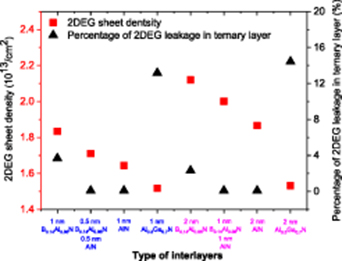
Figure 3. The 2DEG sheet density (red) and the percentage of 2DEG leakage in the ternary layer (black) of the HEMT structures with different configurations of 1 nm interlayers (blue axis) and 2 nm interlayers (purple axis).
Download figure:
Standard image High-resolution imageThough the B0.14Al0.86N interlayer has shown a considerably higher 2DEG sheet density, the leakage of the 2DEG into the B0.14Al0.86N ternary alloy could lead to scattering induced by the alloy disorder, which could compromise the 2DEG mobility and the device characteristics [29]. Meanwhile, figures 2(a) and (c) show that the structures with the 1 nm and 2 nm B0.14Al0.86N interlayers exhibit the highest conduction band edge in the respective figures contributing to large effective conduction band offsets of 4.33 eV and 6.13 eV between the interlayer and the channel, respectively, which is desirable for the suppressed 2DEG leakage. The B0.14Al0.86N/AlN hybrid interlayers result in a slightly lower effective conduction band offset but still higher than that by the conventional AlN interlayers in figures 2(a) and (c). The structures without the interlayer have drastically lower conduction band edge and hence the smallest effective conduction band offset.
Figures 2(b) and (d) manifest the spatial distribution of the 2DEG in the vicinity of the GaN channel. The majority of the 2DEG of all the structures are situated amid the GaN channel, though the structures without the interlayers have the largest leakage of the 2DEG in the Al0.3Ga0.7N ternary layer. To quantify the leakage into the ternary layer, i.e. Al0.3Ga0.7N or B0.14Al0.86N, the percentage of the 2DEG leakage to the ternary layer is defined as follows and the corresponding values are shown by the black triangles in figure 3.

Large percentages of 13.2% and 14.4% are found for the 1 nm and 2 nm Al0.3Ga0.7N (i.e. no interlayer), which can lead to severe alloy scattering. The percentages for the 1 nm and 2 nm AlN interlayers are less than 0.1%, which show effective leakage suppression. Small percentages less than 0.1% are also found for the 1 nm and 2 nm B0.14Al0.86N/AlN hybrid interlayers, indicating excellent suppression with larger 2DEG sheet densities as compared with the AlN interlayers. For the 1 nm and 2 nm B0.14Al0.86N interlayers with the largest 2DEG sheet densities, relatively small percentages of 3.7% and 2.3% are found.
3. HEMT device characteristics
The HEMT device characteristics are investigated subsequent to the study of the 2DEG characteristics. From figure 4, the threshold voltages under VDS = 10 V for the HEMTs with the interlayers of 1 nm B0.14Al0.86N, 0.5 nm B0.14Al0.86N/0.5 nm AlN, and 1 nm AlN are −5.43 V, −5.18 V, and −5.03 V, respectively, which are inversely proportional to the 2DEG sheet density in figure 4. Similarly, for the 2 nm interlayer designs, the threshold voltages are −6.79 V, −6.27 V, and −5.89 V for the 2 nm B0.14Al0.86N, 1 nm B0.14Al0.86N/1 nm AlN, and 2 nm AlN interlayers. The overall decreased threshold voltages for the 2 nm interlayer designs are attributed to the higher 2DEG sheet densities, in comparison with the 1 nm interlayer designs shown in figure 4.

Figure 4. The threshold voltage Vth of the HEMT structures with different interlayers under VDS = 10 V.
Download figure:
Standard image High-resolution imageThe transfer characteristics under VDS = 10 V are shown in figure 5. The 0.5 nm B0.14Al0.86N/0.5 nm AlN hybrid interlayer exhibits the maximum transconductance gm of 311.36 ms mm−1, compared with 310.00 ms mm−1 for the 1 nm B0.14Al0.86N interlayer and 301.6 ms mm−1 for the 1 nm AlN interlayer. Since the gate length remains the same for all structures of interest, the highest maximum transconductance for the 0.5 nm B0.14Al0.86N/0.5 nm AlN hybrid interlayer indicates improved carrier transport attributed to the minimized 2DEG leakage into the ternary layer and the higher 2DEG sheet density shown in figures 2 and 3. Despite with the 2DEG leakage of 3.7%, the 1 nm B0.14Al0.86N interlayer design yields a larger maximum transconductance as opposed to the conventional 1 nm AlN interlayer. Also the transconductance of 310.00 ms mm−1 for the 1 nm B0.14Al0.86N interlayer is barely lower than that for the 1 nm hybrid interlayer, which could be attributed to the larger 2DEG sheet density. For the structures with the 2 nm interlayers, the hybrid interlayer comprising 1 nm B0.14Al0.86N/1 nm AlN shows the largest maximum transconductance of 304.13 ms mm−1 among the three, compared to the 2 nm B0.14Al0.86N interlayer (300.50 ms mm−1) and the 2 nm AlN interlayer (299.63 ms mm−1). Again, the B0.14Al0.86N-containing interlayers lead to higher transconductance than the AlN interlayer for the 2 nm interlayer design. The larger transconductances show the feasibility of employing B0.14Al0.86N as the entirety or part of the interlayer to enhance the channel carrier transport.
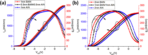
Figure 5. Transfer characteristics under VDS = 10 V of the HEMT structures comprising interlayers of (a) 1 nm B0.14Al0.86N, 0.5 nm B0.14Al0.86N/0.5 nm AlN, and 1 nm AlN; and (b) 2 nm B0.14Al0.86N, 1 nm B0.14Al0.86N /1 nm AlN, and 2 nm AlN.
Download figure:
Standard image High-resolution imageFigures 6(a) and (b) illustrate the IDS−VDS characteristics of the HEMT structures with different 1 and 2 nm interlayers with varying VGS-Vth of +1, +2, and +3 V. In all cases of figures 6(a) and (b), the hybrid B0.14Al0.86N/AlN interlayer results in higher saturation current under the same VGS−Vth, with the HEMTs with the B0.14Al0.86N interlayer and the AlN interlayer being the second and the third, respectively. For instance, the saturation currents for the B0.14Al0.86N/AlN hybrid interlayer and the B0.14Al0.86N interlayer are 5.8% and 2.2% higher than for the AlN interlayer when VGS-Vth = +3 V in figure 6(a) for the 1 nm interlayers. For the 2 nm interlayers in figure 6(b), 3.7% and 1.9% saturation current enhancements are observed in the hybrid B0.14Al0.86N/AlN interlayer and the B0.14Al0.86N interlayer compared with that for the AlN interlayer under the same VGS−Vth. The enhancements are consistent with the enhanced maximum transconductance in figures 5(a) and (b) for the HEMTs comprising the B0.14Al0.86N-based interlayers.

Figure 6. The IDS−VDS characteristics of the HEMT structures comprising interlayers of (a) 1 nm B0.14Al0.86N, 0.5 nm B0.14Al0.86N/0.5 nm AlN, and 1 nm AlN, and (b) 2 nm B0.14Al0.86N, 1 nm B0.14Al0.86N /1 nm AlN, and 2 nm AlN.
Download figure:
Standard image High-resolution image
4. Conclusion
We have proposed the application of the B0.14Al0.86N alloy for the interlayers of GaN-based HEMT device structures. The proposed structures comprise either B0.14Al0.86N interlayers or B0.14Al0.86N/AlN hybrid interlayers of 1 nm or 2 nm thick. The proposed structures lead to considerable enhancement of the 2DEG sheet density as opposed to the conventional AlN interlayers and result in good 2DEG confinement with low 2DEG leakage into the ternary layer. For instance, the structures with the 1 nm B0.14Al0.86N interlayer and the 1 nm hybrid interlayer have 2DEG sheet densities of 1.834 × 10¹³ and 1.710 × 1013 cm−2, which are 11.6% and 4.0% higher than 1.644 × 1013 cm−2 for the 1 nm AlN interlayer, respectively. Additionally, the small percentages of the 2DEG leakage of less than 0.1% are found for the 1 and 2 nm B0.14Al0.86N/AlN hybrid interlayers, indicating excellent suppression with larger 2DEG sheet densities. The enhanced 2DEG characteristics thanks to the use of the B0.14Al0.86N alloy lead to higher maximum transconductance and saturation currents than the HEMTs with the conventional AlN interlayers. As this might be the first work applying BAlN into the III-nitirde HEMT, we believe that there is still huge potential to optimize the HEMT structure with different boron compositions, or using BAlN as the barrier or back barrier layer. Moreover, the experiences of incorporating BAlN alloys into the HEMTs could be transferred to other optoelectronic devices due to their unique polarization and band structure properties, such as UV LEDs, lasers, and photodetectors.
Acknowledgments
The KAUST authors would like to acknowledge the support of like to acknowledge the support of KAUST Baseline Fund Grant No. BAS/1/1664-01-01, GCC Research Council Grant No. REP/1/3189-01-01, and Competitive Research Grant Nos URF/1/3437-01-01 and URF/1/3771-01-01.