
Abstract
Copper foil is the most common substrate to synthesize monolayer graphene by chemical vapor deposition (CVD). The surface morphology and conditions of the copper foil can be very different depending on the various suppliers or different batches. These surface properties of copper strongly affect the growth behavior of graphene, thus rendering the growth conditions irreproducible when different batches of Cu foil are used. Furthermore, the quality of the graphene is severely affected as well. In this work, we report a facile method of copper pre-cleaning to improve the graphene quality and the reproducibility of the growth process. We found that the commercial Ni etchant (based on nitric acid) or nitric acid is the most effective cleaning agent among various acidic or basic solutions. The graphene grown on thus-treated copper surfaces is very clean and mostly monolayer when observed under scanning electron microscopy (SEM) and optical imaging, as compared to the graphene grown on untreated copper foil. Different batches (but with the same catalog number) of copper foil from Alfa Aesar Company were examined to explore the effect of copper pre-cleaning; consistent growth results were obtained when pre-cleaning was used. This method overcomes a commonly encountered problem in graphene growth and could become one of the standard protocols for preparing the copper foil substrate for growing graphene or other 2D materials.
Export citation and abstract BibTeX RIS
1. Introduction
Graphene-based technology has been investigated extensively in the fields of electronics, optoelectronics, and energy storage due to the exceptional properties of graphene such as high carrier mobility, high mechanical strength and optical transparency [1–3]. For many applications, large area graphene film with high quality and uniformity across the whole area is desired [4–8]. Chemical vapor deposition (CVD) on metal substrates has been developed to achieve large area graphene films and Cu foil has been found to be the most effective substrate [9]. Due to a surface mediated growth mechanism, monolayer graphene can be synthesized on Cu foil with low pressure CVD. In recent years, efforts to improve the quality of graphene grown on copper foil by CVD have progressed, for example by increasing the crystalline size, controlling the nucleation site, and understanding the growth mechanism by controlling the growth parameters (pressure, precursor, temperature, and growth time) [10, 11]. Nevertheless, there are still unsolved issues and challenges. In particular, it has been commonly observed under scanning electron microscopy (SEM) that white impurity particles exist on the surface of the copper foil or the graphene after the CVD growth. These impurity particles cause serious problems, such as causing discontinuities in the graphene and increasing the occurrence of multilayer graphene since some of the impurity particles serve as multilayer graphene nucleation sites [12]. Depending on the supplier or the specific batch, the amount of these impurity particles can be quite different. Furthermore, the graphene growth conditions were found to be irreproducible if a different batch of Cu foil is used. These issues have been commonly observed [12–14]5, but not understood well. In this work, we have found that these impurities are mostly on the Cu foil surface before the CVD growth, and can be removed by a facile copper surface cleaning method to allow reproducible synthesis of clean and continuous monolayer graphene. We found that the commercial Ni etchant (Nickel Etchant TFB, Transense) or nitric acid is the most effective cleaning agent among various acidic or basic solutions. Energy-dispersive x-ray spectroscopy (EDX) in SEM and Auger electron spectroscopy (AES) have revealed that the white impurity particles are mainly Si, Ca, Pt, Ru, and Ce. As the copper surface is etched away by nitric acid, the generated NO2 gas bubbles help to push the impurity particles away from the copper surface, leading to a clean copper surface. The graphene grown using the thus-treated Cu foils has been shown to be very clean and continuous and the growth conditions become consistent.
2. Experimental details
2.1. Graphene growth procedure
Graphene was synthesized by low pressure chemical vapor deposition using a copper foil (25 μm, 99.8%, Alfa Aesar) as a catalytic metal substrate. After the pre-cleaning process, the copper foil was annealed at 1000 ° C for 30 min under a 10 sccm hydrogen atmosphere (∼330 mTorr) to increase the grain size and to obtain a smooth surface, followed by graphene synthesis under 5 and 10 sccm of methane and hydrogen atmospheres for 40 min (∼450 mTorr) while maintaining the same temperature. During the cooling of the chamber, 10 sccm of hydrogen was flowed until the furnace was cooled to room temperature.
2.2. Transfer
After the growth, the graphene was transferred from the copper to a SiO2/Si substrate. Poly(methyl methacrylate) (PMMA) (4.5% in anisole) was spun onto the sample at 2500 rpm for 1 min, followed by etching the copper with copper etchant (CE-100, Transene). The film of PMMA/graphene was then washed with DI water. To further remove the residual iron particles which come from the copper etchant (FeCl3), the film was floated on 10% HCl for 20 min, followed by neutralization with deionized water. After the PMMA/graphene was transferred onto the target substrate, the PMMA was removed by acetone vapor.
2.3. Characterization
The sheet resistance values of the graphene films (1 × 1 cm2) were obtained using the van der Pauw method. The Hall voltage to extract the carrier concentration was measured with a magnet of 2000 G. To observe the surface morphology, high resolution field emission scanning electron microscopy (HRSEM, SUPRA™ 40, Zeiss) was used. The surface morphology of the copper foil was examined by atomic force microscopy (Dimension 3100, Veeco).
2.4. Etching test
To estimate the continuity of the graphene films, copper etching tests were carried out. A drop of copper etchant (APS, Transene) was put on a graphene/copper foil for 5 s, followed by washing with DI water and blowing with N2 gas to dry off the water. If the graphene layer does not completely cover the copper surface, the copper etchant will leak through, which results in etching pits on the surface.
3. Results and discussion
3.1. The pre-cleaning process
Figure 1 compares the results of graphene growth with and without the Cu pre-cleaning step. In figure 1(a), SEM images of graphene grown on pristine copper foils (referred to as G-pristine Cu) of the same batch purchased from Alfa Aesar, but from four different runs under the same growth conditions, are shown. As mentioned previously, many white impurity particles with a large variation of size (10 nm–2 μm) can be seen in figure 1(a) (I shows the larger ones, in II–IV these particles can also be seen). Using SEM with energy-dispersive x-ray spectroscopy (EDX) (figure S1(a) available at stacks.iop.org/Nano/24/365602/mmedia) and Auger electron spectroscopy (AES) (figures S1(b) and (c) available at stacks.iop.org/Nano/24/365602/mmedia), it was found that these white particles on the copper surface are mostly metal particles, such as Si, Ca, Pt, Ru, and Ce. These impurities appear to play two roles during graphene growth: (1) as possible nucleation sites for mono- and bilayer graphene growth (for example, in figure 1(a), II and III, it can be seen there are white particles in the center of the bilayer graphene flakes) and (2) as possible obstacles to prevent continuous graphene growth (for example, in figure 1(a), III, the white thin lines are the incomplete graphene regions; some white particles can also be found in these regions; and in figure 1(b), I, the incomplete graphene region (when transferred onto SiO2/Si substrate) is very likely due to the presence of the impurity particles which prevent graphene from growing underneath). Figure 1(b) shows the optical images of graphene grown on these pristine copper substrates transferred to 300 nm SiO2/Si substrates (see SI method, available at stacks.iop.org/Nano/24/365602/mmedia). Figure 1(b) I corresponds to an incomplete region where graphene growth was hampered by the presence of impurity particles. In this region the graphene was not complete due to the presence of impurity particles, whereas in figure 1(b) II there are many broken regions in the graphene film. In our experiments, it appears that the graphene grown on the pristine copper foil tears more easily during transfer.
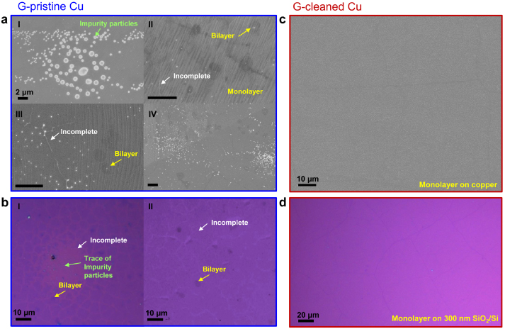
Figure 1. (a) Representative SEM images of graphene grown on different pristine copper foils (purchased from the same batch) using the same growth conditions. The regions of the impurity particles and bilayer graphene, and the incomplete area (no graphene) are clearly observed. (b) Optical images of regions in the corresponding graphene on 300 nm SiO2/Si. Certain incomplete or broken areas and bilayer regions are indicated by the white and yellow arrows, respectively. (c), (d) SEM and optical images of graphene grown on cleaned copper foil and on 300 nm SiO2/Si after transfer, respectively. No impurity particles could be seen and the graphene film has high continuity.
Download figure:
Standard image High-resolution imageThere are two possibilities for the origin of these impurity particles. First, they could come from impurities distributed inside the copper foil and be driven out to the surface during the high temperature growth. Another possibility is that these impurity particles are on the Cu surface even before the CVD synthesis. To test which possibility is dominant, we used various etchant solutions to etch the Cu surface, and found that the impurity particles were significantly removed when Ni etchant (or nitric acid) was used. This suggests that the impurity particles have been on the Cu surface from the beginning (further discussion is presented later in this work). Figure 1(c) shows the SEM image of graphene synthesized on a pre-cleaned copper foil (referred to as G-cleaned Cu). A very clean and highly continuous film can be seen. In addition, the occurrence of bilayer graphene is much reduced. The optical image of this graphene transferred to 300 nm SiO2/Si also confirms highly continuous graphene film (figure 1(d)). From these images it is very clear that the Ni etchant pre-cleaning is very effective in removing the impurity particles on the surface. Furthermore, the synthesis results with different batches of Cu became reliable when the pre-cleaning step was used.
In figure 2, a schematic diagram of the copper pre-cleaning process is shown (figure 2(a)) together with the SEM characterization of the corresponding Cu foil surface at each stage (figure 2(b)). As mentioned previously, our hypothesis is that most of the impurity particles were on the Cu surface. To remove these impurities, the foil was briefly dipped in Ni etchant solution for 30–90 s depending on the amount of impurities observed (see figure S2 available at stacks.iop.org/Nano/24/365602/mmedia). (Note: we have observed that Cu foil having more impurities requires a longer surface cleaning time. However, if the cleaning time is more than 2 min, the copper foil becomes severely damaged and is not useful for growth of graphene.) The main component of the Ni etchant is nitric acid, which reacts with Cu according to


Figure 2. (a) Schematic diagram of the copper pre-cleaning process with Ni etchant. (b) SEM images of the Cu surface corresponding to each step. After copper pre-cleaning, the copper surface is roughened. However, after thermal annealing, the copper surface becomes smooth.
Download figure:
Standard image High-resolution imageDuring this reaction, the Cu on the surface is being oxidized and dissolved in the solution; at the same time NO2 gas is violently generated, helping to push the impurity particles away. In this way, the original surface of the Cu foil, together with the impurities, is scraped off and a new, clean but very rough surface is obtained. After cleaning, the copper foil is dipped in DI water for further washing. This washing process is carried out three times, each time with fresh DI water. It should be noted that this step is very important because if any residual material from the solution is left on the copper surface, these impurities affect the graphene growth as further nucleation sites. To remove the DI water from the copper completely, the copper foil is briefly washed with acetone and isopropanol and dried by blowing with N2. The rough copper surface turns into a clean and smooth surface after postannealing under a hydrogen atmosphere, and is ready for growth of graphene.
In our experiments, various acidic and basic etchants were used to clean the copper foil, such as acetic acid, hydrochloric acid, chromium etchant (Chromium Etchants 1020, Transense), nitric acid, and sodium hydroxide. The SEM images in figure 3 show the copper surface after treatment with several etchants followed by the graphene growth. We found that nitric acid (5.4% (w/w)) and Ni etchant are most successful in removing the impurity particles, whereas the other etchants are not as effective. With acetic acid treatment, there is also a dark region along the copper rolling line (figure 3(a)). We confirmed that the dark regions are not bilayer graphene after transfer to 300 nm SiO2/Si. These regions might be related to the residuals from acetic acid or some impurities. In table S1 (available at stacks.iop.org/Nano/24/365602/mmedia) the etching ability of each etchant is tabulated. Since it was found that the impurity particles contain Si, we used NaOH to clean the copper substrate to remove the Si. However, after NaOH treatment and graphene growth we still found Si impurities on the graphene/copper surface. There could be two reasons why nitric acid (or Ni etchant) is more effective than other etchants. First, it is a strong reactant and oxidizing agent, and can remove many different types of impurities. Second, during the etching, NO2 bubbles are vigorously generated, thereby effectively preventing the impurities from depositing back on the Cu surface. The latter reason could be more crucial to result in effective cleaning.
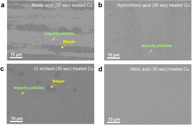
Figure 3. The cleaning effect of various etchants: (a) acetic acid, (b) hydrochloric acid, (c) chromium etchant, and (d) nitric acid. Nitric acid presents a very similar result to Ni etchant.
Download figure:
Standard image High-resolution imageDifferent cleaning times were also investigated to obtain optimized results. In general, we found that 30 s was long enough to obtain a clean graphene surface, while with shorter times typically the white impurity particles were not completely removed (figure S2 available at stacks.iop.org/Nano/24/365602/mmedia). Nevertheless, it was also found that for certain batches of copper foil, the amount of impurity particles is much larger and requires a longer cleaning time. This is illustrated in figure S3 (available at stacks.iop.org/Nano/24/365602/mmedia), where Cu foils from two different batches (but with the same catalog number, Alfa Aesar, 25 μm, 99.8%) are shown for comparison. Even though the foils have the same purity (99.8%), after graphene growth it can be seen that batch I has a lot more impurity particles compared to batch II, both in SEM (figures S3(a) and (c) available at stacks.iop.org/Nano/24/365602/mmedia) and in AFM (figures S3(b) and (d) available at stacks.iop.org/Nano/24/365602/mmedia). It was found that a longer cleaning time (90 s) with simultaneous ultrasonication was necessary to obtain a reproducible clean surface for batch I while 30 s was long enough for batch II.
3.2. Characterization of the graphene grown from the cleaned copper substrates
To evaluate the continuity of the as-grown graphene, we carried out a simple etch test using copper etchant (APS-100, Transense) on the graphene/copper surface [15]. After the CVD growth, if the copper surface is not completely covered by graphene, the copper etchant will leak through the openings and etch the copper underneath (as illustrated by the schematic diagram in the lower insets of figures 4(a) and (b)). For comparison, graphene samples grown from a pre-cleaned copper substrate (figure 4(a), G-cleaned Cu) and from a pristine copper substrate (figure 4(b), G-pristine Cu) were characterized by this method side by side. Figure 4(a) shows a typical AFM height image of G-cleaned Cu after the etching test; no etch pits could be found on the surface, indicating that graphene is highly continuous when grown using these pre-cleaned copper substrates. On the other hand, it can be seen in figure 4(b) that there are many etch pits for the graphene sample grown using a pristine copper substrate. This observation is consistent with the understanding that the impurity particles on the copper surface prevent the graphene film from closing up to form a seamless layer [15].
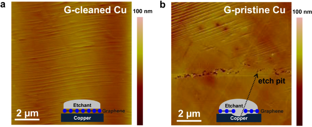
Figure 4. Graphene continuity examination I. AFM images of (a) Ni etchant cleaned copper foil and (b) pristine copper foil after the etching test with Cu etchant (APS-100, Transene) (see section 2.4 for details). The schematic diagrams in the lower inset show the mechanism for generated pits on copper foil.
Download figure:
Standard image High-resolution imageThe quality and continuity of the graphene were further examined by Raman characterization. Figures 5(a) and (b) display the Raman map of G-band intensity (1590 cm−1) divided by Si peak intensity (520 cm−1) for a 50 μm × 50 μm area for G-cleaned Cu and G-pristine Cu transferred to 300 nm SiO2/Si, respectively. The color of the Raman map for the G-cleaned Cu film shows good uniformity over the whole area (figure 5(a)), and this is typical for all G-cleaned Cu samples. On the other hand, it is more common to observe broken graphene regions in the G-pristine Cu samples, and one of these regions is characterized in figure 5(b). As can be seen, the broken regions in the graphene film also result in folded or rolled-up regions. Figures 5(c) and (d) present the corresponding Raman spectra of specific sample positions in figures 5(a) and (b), respectively. It is noted that the D-band in the Raman spectra of both samples is quite low, indicating the good crystalline structure of the graphene samples.

Figure 5. Graphene continuity examination II. Raman mapping images (IG/ISi) of (a) G-cleaned Cu and (b) G-pristine Cu on 300 nm SiO2/Si. For graphene grown on pristine (untreated) copper, it is more common to have tears in the film during transfer. In (b) a region with such tears can be seen. (c), (d) The corresponding Raman spectra of (a) and (b), respectively.
Download figure:
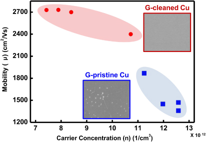
Standard image High-resolution imageElectrical measurements were also carried out to characterize the effect of copper cleaning. Figure 6 shows the mobility versus the carrier concentration for the G-cleaned Cu samples (red circles) and G-pristine Cu samples (blue squares). The mobility carrier concentration values were obtained by Hall measurements using large area samples (1 × 1 cm2). Most G-cleaned Cu samples have high carrier mobilities and low carrier concentrations, whereas G-pristine Cu samples show lower mobilities and high carrier concentrations. The difference in the carrier concentrations for these two types of samples could come from the fact that there are more broken regions in the G-pristine Cu samples with a lot of active edge sites to be doped during the graphene transfer, whereas the basal plane of graphene is not easily functionalized or doped compared to the edges of graphene [16]. In addition, the sheet resistance values of the G-cleaned Cu are between 241 and 295 Ω/sq, whereas the G-pristine Cu samples have a much wider sheet resistance variation, between 368 and 650 Ω/sq. The higher sheet resistance values and their larger variation in magnitude could be due to the fact that G-pristine Cu has more incomplete/broken regions in the film.
Figure 6. Comparison of the graphene carrier mobility and carrier concentration for graphene grown on cleaned versus pristine substrates. The data points of the upper left side and lower right side are obtained from G-cleaned Cu and G-pristine Cu (1 × 1 cm2 size), respectively. Each SEM image of graphene in the inset presents the graphene on a copper surface.
Download figure:
Standard image High-resolution image
Finally, it is worth pointing out that this pre-cleaning method is very effective in removing the impurity particles on the Cu surface allowing the growth of continuous graphene with higher quality and reproducibility. As some of these impurity particles also serve as nucleation sites for the growth of bilayer or multilayer graphene, this method can also help to reduce the amount of bi- or multilayer graphene. However, the bilayer or multilayer growth cannot be completely eliminated, since this growth is also determined by the growth conditions. Further effort is still needed to gain better control over the growth of monolayer versus bilayer or multilayer graphene.
4. Conclusion
In this work, we presented a facile method to clean copper foil before graphene growth. The common impurity particles on the Cu foil are found to be Si, Ca, Pt, Ru, and Ce. Among the various etchants, Ni etchant (or nitric acid) is the most effective cleaning agent. As a result, we obtained clean, continuous, and higher quality graphene by CVD. This method also helps to produce graphene with better reproducibility. This result will be highly desirable in many applications, not only for devices but also for oxidation resistance layer or impermeable atomic membrane applications as well [17, 18]. Since copper foils are also commonly used as substrates for the growth of other 2D materials, this method should be applicable to these applications as well [19–21].
Acknowledgments
This work is partially supported by the National Science Foundation under award number NSF DMR 0845358 and the Materials, Structures and Device (MSD) Center, one of the five programs in the focus center research program (FCRP), a Semiconductor Research Corporation program. A Hsu acknowledges the support from the MIT/Army Institute for Soldier Nanotechnologies (ISN). K K Kim acknowledges the support from the Leading Foreign Research Institute Recruitment Program through the National Research Foundation of Korea (NRF) funded by the Ministry of Education, Science and Technology (MEST) (No. 2012-00109). J Kong and M S Dresselhaus acknowledge the Graphene Approaches to Terahertz Electronics (GATE)—MURI grant N00014-09-1-1063. This work was also partially supported by the Korea Institute of Science and Technology (KIST) Institutional Program.
Footnotes
- 5
Discussions among our own group with other groups at the University of Southern California, and the University of Illinois at Urbana Champaign.