

Abstract
This paper reports photosensitive organic–inorganic hybrid polysiloxane (Poly-SX) based passivation fabricated at low temperatures under 180 °C for high performance and highly reliable amorphous InGaZnO (a-IGZO) TFT. The Poly-SX passivation can be fabricated by solution and photolithography process without needing any dry etching process. The passivated a-IGZO TFT has a high field effect mobility reaching 10.91 cm2 V−1 s−1 and enhanced reliability with a threshold voltage shift as low as +2.0 and −0.9 V after positive (PBS) and negative bias stress (NBS), respectively. These results demonstrate the possibility of fabricating passivated a-IGZO TFT on various flexible organic substrates at low temperatures by solution process.
Export citation and abstract BibTeX RIS
High performance thin film transistor (TFT) using amorphous InGaZnO (a-IGZO) is gaining a lot of attention in next generation flat panel displays, liquid crystal display (LCD), organic light emitting diode (OLED), and quantum dot light emitting diode (QLED). Devices that incorporate a-IGZO TFTs are popular because it has high transparency, large area uniformity, low temperature processability and excellent electronic properties such as high electron mobility, low off-current, low threshold voltage (Vth), small subthreshold swing (S) and good stability after bias stress.1,2) However, a-IGZO TFTs have reliability issues such as instability after positive bias stress (PBS) and negative bias stress (NBS).3) To reduce the degradation from atmosphere such as hydrogen, oxygen and water, which generate shallow charge trapping sites for electron,2,3) the a-IGZO backchannel is protected by inorganic passivation material such as SiO2, SiN, MgO, TiOx, Y2O3, Al2O3, and HfO24–6) fabricated by plasma enhanced chemical vapor deposition (PE-CVD) process and atomic layer deposition (ALD) process. ALD is a good method for fabricating pure dielectric layers, such as thermal ALD AlOx,7) sputtered Al2O3,8) and ALD Y2O3,9) double-layer passivation, such as Al2O3/SiNx10) and Parylene/Al2O3.11) These inorganic films fabricated by vacuum process have good passivation property, but the fabrication processes are usually complicated and utilize high temperature processes (>400 °C) to fabricate fine and uniform films. Previous research have shown organic passivation materials such as B-staged bis(benzocyclobutene) based resin,12) paraffin wax,13) CYTOP,14) poly(dimethylsiloxane) (PDMS)15) that can be fabricated by solution process. We have also previously reported solution processed organic and inorganic hybrid Poly-SX.16) Solution processed materials have the advantage of the capability of coating very uniform films in a large area. In addition, it can be used in an additive process such as printing which reduces material utilization and thus reducing cost.
Recently, a-IGZO was applied in the backplane of OLED and QLED for flexible devices. These applications typically require a low temperature process to enable fabrication on organic films. A typical disadvantage of most organic passivation is the high temperature process (>300 °C) needed to remove unwanted components in the precursor and to condense the passivation film. Table I shows the performance of passivation materials which have been reported in the past for a-IGZO TFT by solution process. To address this high temperature issue, organic passivations,13,14) PDMS,15) solution processed HfO217) and our non-photosensitive Poly-SX18) have been recently shown to be suitable candidates for application of advanced flexible display because these are fabricated using a low temperature solution process (<200 °C). Furthermore, the electrical characteristics of Poly-SX passivated TFTs can be enhanced by excimer laser annealing without thermal annealing.19) However, during the fabrication of these passivation materials, the electrical characteristics and performance are degraded due to the plasma damage by reactive ion etching (RIE), when contact holes on the source and drain are formed to contact the electrodes. Also, PDMS which consists of a D type structure (RSiO) is known to generate low molecular weight cyclic silicone20) which is a cause of contact fault in devices after baking. We have previously reported photosensitive Poly-SX passivation which can form contact holes through a simple photolithography process without any RIE process.21) This passivation improved the electrical property and showed high reliability after bias stress. Poly-SX which is mainly composed of SiO bond, not only exhibit excellent passivation properties but also possess substantial chemical durability against thinner, etchant and resist strippers usually used in subsequent fabrication processes compared with other organic passivation materials. However, these photosensitive passivation materials were fabricated at a high temperature of 300 °C which is not compatible with most flexible substrates. In this paper, we report a highly reliable photosensitive Poly-SX passivation for a-IGZO TFT despite curing at low temperature (180 °C) and clarified the effect of the passivation process to the channel layer. The decrease in process temperature without the loss of the photosensitivity will significantly help in not only inhibiting potential sources of degradation but also in reducing the process cost of developing next-generation flexible devices.
Table I. Summary of fabrication temperature, process, and ΔVth after PBS of each passivation materials.
| Paraffin13) | CYTOP14) | HfO217) | MePhQ50401018) | P-PSQ21) | |
|---|---|---|---|---|---|
| Cure temp. | RT | 180 °C | 150 °C | 180 °C | 300 °C |
| Process | No description of contact hole fabrication(Actual device usually need dry etching) | Dry etching | Photolithography | ||
| ΔVth after PBS | <1.0 V Vgs = 30 V, 1000 s at 30 °C | 2.8 V Vgs = 20 V, 5000 s Vds = 0 V at 30 °C | 1.68 V Vgs = 20 V, 10000 s Vds = 10.1 V | 0.9 V Vgs = 20 V, 10000 s Vds = 0 V at RT | 0.5 V Vgs = 20 V, 10000 s Vds = 0 V at RT |
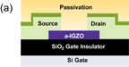
Figure 1 shows the cross section image of the bottom gate and top contact a-IGZO TFTs used in this study. The a-IGZO channel layer was deposited on a thermally oxidized SiO2/highly conductive n-doped Si substrate by RF magnetron sputtering deposition at room temperature. The channel thickness was 70 nm, which was deposited from sputtering a target of a-IGZO with a stoichiometric ratio of  . After channel patterning via photolithography, source and drain electrodes of Mo/Pt (80/20 nm) were deposited using RF magnetron sputtering and pattern through a lift-off process. Post annealing process for all TFTs was carried out at 300 °C for 2 h in N2/O2 (
 ) ambient atmosphere. We used these TFTs annealed at 300 °C to focus on the evaluation of passivation properties fabricated by low temperature process. After that, Poly-SX passivation layer was fabricated by solution process on the a-IGZO TFT. After coating 1.5 µm of Poly-SX, this layer was prebaked at 100 °C for 90 s to evaporate the solvent. In this research, we used a negative type photosensitive Poly-SX which can be cured by UV light to form contact holes (Fig. 2). This photosensitive fabrication can reduce the number of process from 10 to 6 steps compared with the fabrication of non-photosensitive passivation. The reduction of process steps especially skipping steps which can potentially induce degradation such as resist deposition, dry etching, and resist stripping promotes the high throughput fabrication of highly reliable TFTs. The exposed area of negative Poly-SX layer was initially cured by UV light and baked additionally at 120 °C for 60 s to facilitate further curing. Then, contact holes were formed at the unexposed area after development by TMAH 2.38% water solution. These TFTs were post-baked at 180 °C for 1 h in ambient atmosphere after exposure to UV light with sufficient energy over 200 mJ/cm2 to cure the passivation material via formation of the SiO bonds. Finally, the Poly-SX passivated a-IGZO TFTs were post-annealed at 150 °C for 2 h in O2 ambient atmosphere.
Download figure:
Standard image High-resolution image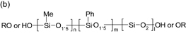
Fig. 1. (a) Device structure of bottom gate a-IGZO TFT passivated by Poly-SX. (b) Main polymer structure of evaluated Poly-SX. Terminal functional group of the Poly-SX includes OH and alkoxyl group.
Download figure:
Standard image High-resolution image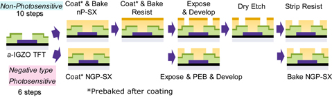
Fig. 2. Fabrication process of non-photosensitive Poly-SX and Negative type photosensitive Poly-SX with contact hole on a-IGZO TFT (Poly-SX: light yellow, resist: yellow).
Download figure:
Standard image High-resolution imageTwo types of photosensitive Poly-SX material were evaluated for passivation of a-IGZO TFTs (Fig. 1 and Table II). NGP-SX 1 and 2 are Poly-SX which is a combination of methyl (Me) 50%/phenyl (Ph) 40%/SiO2 (Q) 10% (MePhQ504010) and Me 70%/Q 30% (MeQ7030), respectively. These Poly-SXs was synthesized by polycondensation of silane monomers with an alkali catalyst. The polymer structure is mainly controlled by the functional group of Si and the amount of catalyst and water.22) These functional groups influence the mechanical and chemical properties of the passivation.18) MeQ7030 which includes a higher ratio of inorganic structure has a highly dense structure, hardness, chemical durability, and reactivity at low temperature from silica (Q) structure. In this research, we used a different type of MePhQ504010 compared with the previous report.18) NGP-SX 1 included a high silanol type of MePhQ504010 to enable dissolution by an alkali developer. Water based alkali developer was preferred compared with organic solvent for environmental protection. NGP-SXs coated films have negative-type photosensitivity from photo initiator which accelerates the silanol condensation at the exposed area. The film at the unexposed area was dissolved by the alkali developer to form the contact holes. These two types of Poly-SXs have a suitable amount of silanol to enhance the development time.
Table II. Main polymer and Monomer formulation of NGP-SXs. n, m, and l denote the mol % of the methyl, phenyl, and silica groups, respectively.
| Sample | Polymer | n | m | l | Photolithography |
|---|---|---|---|---|---|
| NGP-SX 1 | MePhQ504010 | 50 | 40 | 10 | Yes |
| NGP-SX 2 | MeQ7030 | 70 | — | 30 | Yes |
Table III shows the transparency and electrical properties of NGP-SX 1 and 2 after UV curing and thermal curing at 180 °C for 1 h in ambient atmosphere. With a transparency of 99% in the visible region (at 400–800 nm), these materials have excellent transparency for display applications. The dielectric constants of NGP-SX 1 and 2 are 3.72 and 3.93, respectively, which are similar to thermal oxide SiO2. Also, the leakage current at 2 MV/cm of NGP-SX 1 and 2 are 4.6 and 0.60 µA, respectively.
Table III. Summary of dielectric constant and leakage current of each sample.
| Sample | Transparency at 400 nm | Dielectric constant | Leakage current at 2 MV/cm (µA/cm2) |
|---|---|---|---|
| NGP-SX 1 | >99% | 3.72 | 4.6 |
| NGP-SX 2 | >99% | 3.93 | 0.60 |
The initial characteristics and reliability after PBS and NBS of these NGP-SX passivated TFTs were evaluated with a semiconductor parameter analyzer (Agilent 4156C) at room temperature. The size of the channel length and width were 10 and 90 µm, respectively. The passivated TFTs were subjected to PBS by applying a gate voltage of (Vgs = 20 V) and NBS (Vgs = −20 V) for 10000 s with Vds = 0 V at room temperature.
We compared the device properties between two types of passivated TFTs and un-passivated TFT (Fig. 3). The transfer characteristics (Ids–Vgs) of passivated TFTs show clear transfer curves and exhibit no hump phenomenon despite being cured at low temperature, because these passivation materials have good barrier property from water in air compared with un-passivated TFT. Electrical characteristics are obtained from the transfer characteristics in the linear regime at Vds = 0.1 V using
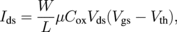
where Cox is the capacitance and the field effect mobility (μ) is obtained from
where gm is the measured transconductance.
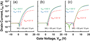
Fig. 3. Initial characteristics (absolute value) of (a) un-passivated and (b) passivated a-IGZO TFT by NGP-SX 1, (c) NGP-SX 2.
Download figure:
Standard image High-resolution imageThe μ of un-passivated, passivated NGP-SX 1 and 2 were 7.39, 6.93, and 10.91 cm2 V−1 s−1, respectively (Table IV). Particularly, the μ of NGP-SX2 increased by 48% from un-passivated TFTs and a higher μ compared with non-photosensitive Poly-SX.18) This is because the photosensitive Poly-SX passivation can form contact hole patterns via photo-lithography without RIE process which is known to damage TFTs. Also, NGP-SX was cured gradually through a 2 step process of UV exposure/soft bake to accelerate the reaction to form contact holes and post bake process. The gradual 2 step process can further reduce the remaining impurities which degrade TFT performance which is better than the drastic curing performed with non-photosensitive Poly-SX. In addition, Poly-SX film fabricated by this 2 step process causes a slightly lower residual stress on TFT. The residual stress has been shown to degrade the TFT performance.23) The Vth of NGP-SX 2 decreased from 6.50 to 3.37. Also, NGP-SX 2 has lower subthreshold swing (S) compared with other TFTs. Figure 4 exhibits the reliability of Poly-SX passivated a-IGZO TFTs after bias stress. The ΔVth of NGP-SX 1 and 2 under PBS/NBS after 10000 s were +2.0 V/−0.9 V and +2.4 V/−1.8 V, respectively. In this research, NGP-SX 1 and 2 were baked at lower temperature (180 °C). Nevertheless, the NGP-SXs show lower ΔVth and higher reliability compared with un-passivated TFT (+6.2 V/−2.6 V).21) The NGP-SXs passivated TFT has comparable device performance with positive photosensitive Poly-SX cured at a higher temperature of 300 °C.21) One of the causes of the enhanced property is that NGP-SXs have a simple formulation that circumvents RIE thus inhibiting etching damage on the TFT and include lower amount of carbon from photo active compounds. Generally, controlling the carbon amount is also important for a-IGZO TFT due to performance degradation by a high amount of carbon.24) Also, NGP-SX 2 consist of the same polymer with non-photosensitive MeQ7030.18) Both passivated TFTs did not exhibit any hump phenomenon but NGP-SX 2 has a lower ΔVth shift than −4.3 V observed in non-photosensitive MeQ7030 passivated TFT after NBS and higher mobility than 4.33 cm2/V. The improved performance of NGP-SX 2 over its non-photosensitive counterpart can mainly be attributed to its fabrication which consists mainly of a photolithography process without RIE thus inhibiting plasma damage.
Table IV. Summary of electrical characteristics.
| Sample | Mobility (cm2 V−1 s−1) | Vth (V) | S (V/dec) |
|---|---|---|---|
| Un-passivated | 7.39 ± 1.57 | 6.50 ± 0.30 | 0.22 ± 0.03 |
| NGP-SX 1 | 6.93 ± 0.19 | 5.76 ± 0.39 | 0.22 ± 0.08 |
| NGP-SX 2 | 10.91 ± 0.19 | 3.37 ± 0.80 | 0.17 ± 0.05 |
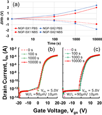
Fig. 4. (a) ΔVth of passivated a-IGZO TFT after PBS (Vgs = 20 V) and NBS (Vgs = −20 V). (b, c) Evolution of transfer characteristics (absolute value) of (b) NGP-SX 1 and (c) NGP-SX 2 after NBS.
Download figure:
Standard image High-resolution imageTo theoretically estimate the value and evaluate the factors which influence Vth shift at longer stress time of a-IGZO TFTs, we used the stretched exponential model,25)

where ΔV0 is the threshold voltage shift at infinite time, this is provided by Vg-stress (applied stress voltage) − Vth-initial (initial Vth before stress), T represents the stress time, τ is the characteristic trapping time of carriers, and β is the stretched-exponential exponent. Figure 5 shows the fitting curve from the equation. The τ/β value of NGP-SX 1 under PBS and NBS were 0.48 × 10⁶/0.36 and 3.10 × 10⁸/0.31, respectively. In the case of NGP-SX 2 under PBS and NBS, the values were 6.53 × 10⁶/0.29 and 3.98 × 10⁶/0.40, respectively. The coefficient of determination (R2) of all NGP-SX passivated TFTs are very high over 0.95 and shows a very good fit. The result showed that the degradation mechanism is mainly due to charge trapping and injection rather than other degradation mechanism such as defect creation and impurities.26)
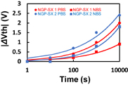
Fig. 5. ΔVth of passivated a-IGZO TFT by NGP-SX 1 (red) and NGP-SX 2 (blue) after PBS (circle) and NBS (square). Lines show the fitting results to the stretched-exponential functions.
Download figure:
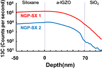
Standard image High-resolution imageWe analyzed the distribution profile of elements in the interface of passivation/a-IGZO layer and the bulk of a-IGZO layer by secondary ion mass spectrometry (SIMS). NGP-SX 2 showed a lower amount of carbon by −93% compared to NGP-SX 1 (Fig. 6). NGP-SX 1 have a higher amount of carbon due to its methyl and phenyl functional groups in the Poly-SX structure. Carbon from this passivation layer diffused into the a-IGZO layer and was detected by SIMS. Also, NGP-SX 2 has a lower amount of OH and H compared to NGP-SX 1. This is because in a-IGZO passivated by NGP-SX 2, it was easier for the silanol group to condensate compared to NGP-SX 1 and to decompose the source of OH and H. Additionally, NGP-SX 2 which includes a higher ratio of Q structure in the polymer has a higher density barrier structure against atmosphere than NGP-SX 1.
Fig. 6. SIMS profile of 13C (solid line), 16O+1H (dash line), and 1.2H (dot line) in the interface of passivation/a-IGZO layer, bulk of a-IGZO and the interface of a-IGZO/SiO2 layer of NGP-SX 1 (red) and 2 (blue).
Download figure:
Standard image High-resolution image
NGP-SX 2 passivation has lower amounts of carbon and has a mainly inorganic composition relatively closer to silica because of the Q structure. This passivation has lower carbon diffusion, which causes the higher mobility compared with NGP-SX 1. Additionally, the silica structure of NGP-SX 2 creates a higher density barrier structure from atmosphere and enables the improvement of reliability. It is difficult to form contact holes by RIE for the non-photosensitive MeQ703018) because having a higher density structure increases the etching durability, which causes the TFT to be exposed to longer etch time and incur plasma damage. However, with these photosensitive NGP-SX, the RIE process can be entirely skipped and plasma damage will be inhibited, which promotes a higher device performance.
In this research, we demonstrated high mobility and highly reliable photosensitive passivation for a-IGZO TFT despite baking at a lower temperature under 180 °C. The photosensitive passivation use photolithography process to make contact holes instead of an RIE process. Coating the NGP-SX passivation on the a-IGZO TFT increased the field effect mobility by 48% from un-passivated TFT. Also, the Vth shift was minimized during PBS and NBS to 2.4 and −1.8 V, respectively. These characteristics show the promising applications of photosensitive Poly-SX passivation in a-IGZO TFTs and flexible devices fabricated at low temperature process on various film substrates.