
Abstract
We demonstrate optically-pumped waveguides grown on freestanding GaN substrate featuring AlInN claddings and GaN/Al0.1Ga0.9N multiple quantum wells exhibiting narrow bandwidth (3.8 nm) optical gain around 370 nm. Due to the high refractive index contrast between the cladding layers and the active region, the confinement factor is as high as 48% and net modal gain values in excess of 80 cm−1 are measured. The results agree well with self-consistent calculations accounting for built-in electric field effects and high carrier density related phenomena. These results open interesting perspectives for the realization of more efficient near-UV lasers and optical amplifiers.
Export citation and abstract BibTeX RIS

Content from this work may be used under the terms of the Creative Commons Attribution 4.0 license. Any further distribution of this work must maintain attribution to the author(s) and the title of the work, journal citation and DOI.
Over the past two decades, visible emitting III–nitride (III–N) light-emitting diodes (LEDs) and laser diodes (LDs) emerged as essential optoelectronic devices, which led to the solid-state lighting revolution. This was made possible thanks to their compact and power-efficient nature compared to what offered previous technologies. However, III–N-based UV light sources exhibit decreasing device performance with decreasing emission wavelength.1,2) Although III–N LEDs have been demonstrated with emission wavelengths down to 210 nm,3) the shortest emission wavelength reported to date for conventional edge emitting LDs is 336 nm and in this case, it is limited to pulsed mode operation.4) Shorter wavelength operation requires either optical pumping5) or electron beam pumping.6) Beyond reduced p-type conductivity that results from the increasing activation energy of the Mg-acceptor with increasing band gap, residual absorption occurring in the (Al)GaN cladding layers is an important source of losses and the limited refractive index contrast between the waveguide (WG) and the cladding materials is detrimental to the optical confinement factor (Γ). A potential pathway to decrease the lasing threshold relies on the use of AlInN cladding layers. Indeed, the latter offer a high refractive index contrast with the AlGaN alloy over a wide range of Al contents7,8) leading to efficient vertical confinement for the optical mode, while being grown lattice-matched (LM) to GaN, resulting in very good material quality.9–12) Furthermore, p-type doping of AlInN has been demonstrated13) and high-quality AlInN layers have been successfully used for optical mode confinement in visible III–N edge-emitting LDs.14)
Let us also notice that coherent light emitters operating in the spectral region ranging from 350 to 370 nm have been scarcely addressed compared to their longer and shorter wavelength counterparts based on InGaN/GaN and (Al)GaN/AlGaN multiple quantum wells (MQWs), respectively, despite their potential applications in phototherapy, gas sensing, or UV fluorescence.15)
In this work, we investigate the properties including optical gain from III–N WGs consisting of AlInN cladding layers and GaN/AlGaN MQWs grown on freestanding (FS) GaN substrate, operating near 370 nm at room temperature (RT). They feature a narrow gain band with a full-width at half maximum (FWHM) of ∼20 meV, hence corresponding to limited gain dilution for this material family. The LM claddings lead to structural defect-free structures of high optical quality and high Γ value of 48%. We demonstrate optical gain values in excess of 80 cm−1, a value which is essentially limited by the absorption of the pump laser used in our experiments.
The sample structure is sketched in Fig. 1(a) and consists of a 170-nm-thick active region with 14 GaN/Al0.1Ga0.9N (6.2 nm/4.8 nm) QWs sandwiched between bottom and top Al0.82In0.18N claddings, which are LM to GaN. The bottom cladding layer contains seven 5-nm-thick GaN interlayers positioned 50 nm apart in order to avoid kinetic roughening of the AlInN alloy.11)

Fig. 1. (a) Sketch of the sample structure and (b) scanning transmission electron microscopy (TEM) image of the MQWs taken with a high-angle annular dark-field detector in the ![$[10\bar{1}0]$](https://content.cld.iop.org/journals/1347-4065/57/9/090305/revision1/AP180450RCif001.gif) zone-axis orientation. Inset: High-resolution TEM image of the QWs showing sharp interfaces. (c) Optical mode profile of the TE0 mode supported by the present WG calculated with a commercial FDTD solver.16) Position is determined with respect to the GaN buffer/AlInN bottom cladding layer interface.
zone-axis orientation. Inset: High-resolution TEM image of the QWs showing sharp interfaces. (c) Optical mode profile of the TE0 mode supported by the present WG calculated with a commercial FDTD solver.16) Position is determined with respect to the GaN buffer/AlInN bottom cladding layer interface.
Download figure:
Standard image High-resolution imageThe WG dimensions were chosen to support a single transverse electric (TE) polarized mode to avoid gain competition. This was confirmed by finite-difference time-domain (FDTD) calculations16) where the refractive index for (Al)GaN layers and that of Al0.82In0.18N cladding layers were taken from the work of Brunner et al.17) and Butté et al.,7) respectively. The fundamental TE WG mode (TE0) determined from these calculations is shown in Fig. 1(c). The large refractive index contrast between the MQWs and the AlInN cladding layers of ∼12% at 370 nm results in a small effective length Leff = 99 nm of this mode.18) This, together with the large number of QWs, leads to a high Γ of 48.2%, which is essential to ensure both high modal gain and low lasing threshold. Note, however, that such a high number of QWs cannot be efficiently pumped using an electrical injection scheme mainly due to the limited hole mobility. A similar WG with only 3 QWs near the peak of the modal field would have a Γ value of 17% and would be better suited for electrical injection.
First, we calculated the band diagram of the sample in the one-electron picture as shown in Fig. 2(a).19) The Fermi energy was pinned to the mid-gap at the sample surface20) and the electric field in the QWs was set to ∼300 kV/cm, a value expected from the polarization mismatch between the multilayer constituents that accounts for the geometric effect.21) The residual doping level is difficult to assess for this sample due to the presence of a two-dimensional electron gas (2DEG) at the interface between the MQW region and the top cladding layer. We know however that the typical residual n-type doping levels amount to 5 × 1018 cm−3 in similar AlInN layers9) and ∼1 × 1016 cm−3 in GaN/AlGaN QWs.22)

Fig. 2. (a) Band diagram of the whole structure. (b) LT (T = 11 K) CL cross-section mapping of the QW emission (logarithmic color scale) recorded with an acceleration voltage of 2 kV along with the XA energy of the different QWs as deduced from the combination of the one-electron picture and excitonic effects obtained from a SP-k·p solver (black dots).
Download figure:
Standard image High-resolution imageIn order to ensure a better consistency between calculations and experimental results, we also included excitonic effects by means of a Schrödinger–Poisson-k·p (SP-k·p) solver previously used to account for the Mott transition in single GaN/AlGaN QWs.23) As will be shown hereafter, due to the quantum confined Stark effect (QCSE) and the large QW width, the A exciton (XA) energy in the MQWs is lower than that of bulk GaN.24)
The calculated low temperature (LT) QW exciton energies were first compared to cathodoluminescence (CL) measurements recorded along the cross-section of the sample [Fig. 2(b)]. We observe an increase in the calculated exciton energy from QW1 to QW13 due to a decreasing built-in electric field, which is well-matched by the experiment. The gradual decrease in the electric field results from the band bending caused by ionized donors in the MQWs, which stem from the transfer of electrons into the 2DEG potential at the AlGaN/AlInN top interface. Note however that the top QW (QW14) deviates from this trend and has a lower emission energy and a higher built-in field due to its location near the 2DEG.
To be more quantitative, we investigated the optical properties of the sample by conducting photoluminescence (PL) and polychromatic PL excitation (PLE) experiments at LT. A representative PLE spectrum obtained for an excitation power density of 60 kW/cm2 is shown in Fig. 3. We verified that despite the high excitation power density it did not induce any shift in the exciton energy. In fact, the MQW region remains in the low carrier density regime due to the limited absorption occurring in the QWs for near-resonant excitation below the AlGaN barrier band edge. We observe resonances coming from the three free excitons, which match pretty well the energies deduced from the SP-k·p formalism, as well as weak absorption features ascribed to the n = 2 state from the A and B exciton hydrogen series.25) The measured PLE FWHM of 11 meV for the XA transition corresponds well with the calculated energy spread of QW1 to QW13 shown in Fig. 2(b). The PL spectrum obtained at the excitation wavelength of 355 nm is also shown in Fig. 3. A PL linewidth of 5 meV is measured for the XA QW peak while a Stokes shift (SS) of 2.5 meV is obtained with respect to the PLE peak. These low values compared with those expected from PLE measurements are a consequence of the gradient in the MQW energies discussed above. Indeed, since the top QWs are transparent for the resonant energy of the bottom ones, the entire stack of QWs is probed using PLE. On the contrary, for PL measurements the laser excitation is mostly absorbed in the top QWs and hence emission is dominated by high-energy QWs. This reduces the measured SS and the PL linewidth. This effect is further enhanced for PL experiments where excitation above the barrier band edge is used. Due to the shorter absorption length, PL emission is dominated by fewer QWs. In this case the SS between PLE and PL peaks is reduced to 1 meV. For the same reason, we observe a localization energy of ∼1 meV in PL for temperature series when using non-resonant excitation into the AlGaN barriers. Let us note that the inhomogeneous broadening (γinh) of 5 meV deduced from LT PL measurements is likely inherited from the exciton binding energy EB of 19 meV stemming from the small electron–hole wavefunction overlap of ∼0.2. This EB value translates into a large exciton Bohr radius aB = 5 nm for III–N quantum heterostructures. As a consequence, the exciton wavefunction is spread over a larger volume than for its narrow GaN/AlGaN MQW counterparts, which reduces its sensitivity to well width fluctuations and alloy disorder.

Fig. 3. LT (T = 4 K) PLE spectrum (black line) and corresponding PL spectrum (red line) recorded at an excitation wavelength of 355 nm showing a Stokes shift of 2.5 meV.
Download figure:
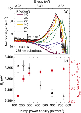
Standard image High-resolution imageThe net modal gain (gmod) was then measured at RT by means of the variable stripe length (VSL) method using a Q-switched frequency-tripled Nd:YAG 355 nm pump laser of large enough fluence [Fig. 4(a)]. Since this laser operates below the barrier band edge, light is only absorbed by the QWs, which ensures nearly homogeneous carrier distribution over the different QWs. The gmod spectra were then fitted using a self-consistent approach accounting for the A and B hole subbands, progressive screening of the built-in field, saturation of the MQW absorption and band gap renormalization with increasing carrier density.23) It allowed extracting the average carrier density per QW, Navg, and the average low carrier density transition energy, E0, which are shown in Fig. 4(b). First, we emphasize that the modal gain is originating from an electron–hole plasma, i.e., a regime that does not involve any excitonic effects, a feature consistent with prior studies.23) Given the specificity of the structure, which is composed of QWs emitting at slightly different energies and subjected to different carrier densities, quantitative modeling of the modal gain seems rather challenging. However, the high structural and optical quality of the sample allows for a precise determination of its properties in the low-density regime, hence minimizing the number of unknown parameters. Note, however, that for the sake of simplicity, we did not include any LO-phonon contribution to the modeling of the gain spectra.26) This latter aspect could therefore account for the discrepancies observed between simulations and experimental data, especially for low pumping fluences. A consequence of this simplification is the use of an increased value by a factor of ∼2 of γinh to obtain good fits, i.e., a value of 20 meV compared to 11 meV as determined through PLE experiments.
Fig. 4. (a) Net modal gain (continuous lines) measured at RT for c-plane GaN/AlGaN MQWs embedded in a WG using the VSL method. Fits relying on a SP-k·p formalism (dashed lines) show a good quantitative agreement with experiments. (b) Parameters extracted from the modeling: low carrier density transition energy (black dots) and average carrier density (red squares).
Download figure:
Standard image High-resolution image
Experimentally, we observe a fast increase in gmod for pump power densities ranging from 220 to 295 kW/cm2. This is ascribed to the large number of QWs and the high Γ value, which allow to reach the transparency regime with a high efficiency under near-resonant excitation. When the pump power density is further increased, the peak modal gain value and the average carrier density exhibit a saturation-like behavior with a peak gmod value of ∼80 cm−1. This is likely originating from the limited pump absorption by the QWs due to efficient band filling. From the absorption saturation term included in the model, we deduce a saturation photon density of 2.7 × 10¹⁴ photons/cm2 = 300 kW/cm2 with the 355 nm pump laser. Additionally, a residual WG absorption loss of 25 ± 5 cm−1 is deduced from gmod spectra [Fig. 4(a)].
We also observe a redshift of the gain band with increasing pump power. This is opposite to the commonly observed blueshift in such experiments.22,27) This spectral shift can be accounted for by considering two of the phenomena at play, namely band filling and the shift of the transition energy Etr with increasing carrier density N. The latter is indeed given by

where E0 is the transition energy measured at low carrier density, ΔEQCSE(N) is the energy shift due to progressive screening of the built-in field with increasing carrier density and ΔEBGR(N) is the energy shift due to band gap renormalization.
Let us briefly discuss the weight of the different contributions. Band filling will cause a blueshift of the emission with increasing carrier density, which is mainly dependent on the γinh value of the MQWs. Indeed, systems characterized with a large γinh, such as InGaN/GaN QWs emitting in the visible22) or AlGaN/AlGaN QWs emitting in the deep UV27) will experience a much larger blueshift than a system with low inhomogeneity such as the present MQW structure. Band filling is well accounted for by the model used here.23) QWs subjected to a built-in field will experience the usual blueshift observed with increasing carrier density that can be determined using a self-consistent SP solver.23) Band gap renormalization arises from interparticle interactions and was accounted for by the relationship introduced by Schmitt-Rink et al.28)
E0 was kept as a fitting parameter in the model whose value as a function of power density is shown in Fig. 4(b). We notice a redshift of ∼14 meV of magnitude comparable to the MQW energy spread shown in Fig. 2(b). This indicates that the lower-energy QWs have an increasing relative weight in the gmod spectra with increasing pump power. Indeed, due to the larger saturation experienced by the blue emitting top QWs, the red emitting bottom ones will be more efficiently populated at higher pump power, hence explaining the overall redshift of the gain band. Nonetheless, it is worth mentioning that this moderate shift of the gain band could prove useful for the realization of devices where the output power needs to be varied with minimal changes in the output wavelength such as semiconductor optical amplifiers (SOAs).
In addition, the emission wavelength of this type of structures could be easily tuned toward the 350 nm spectral range by decreasing the QW thickness, without any loss in material quality.12) We would also expect reduced transparency and lasing thresholds in samples with thinner QWs due to the smaller weight of the QCSE and hence the larger overlap between electron and hole wavefunctions.
In conclusion, we have reported on high-quality LM WGs with AlInN claddings and a GaN/AlGaN MQW active region grown on FS GaN substrate. Thanks to the large refractive index contrast between the core and the cladding layers, a Γ value as large as 48% is achieved. It is shown that the complex interplay between the spontaneous polarization mismatch between the claddings and the MQW region together with the residual doping in the active region leads to a gradient in the built-in field and hence a change in the transition energy of the different QWs. This gradient appears to be the main source of inhomogeneous broadening in this sample. The measured gmod is successfully reproduced using a SP-k·p formalism and gmod values in excess of 80 cm−1 are reported whose value is limited by absorption of the near-resonant pump laser. Due to the small disorder in the sample, the gain band is as narrow as 20 meV. It exhibits a small redshift with increasing pump power, which is a consequence of the QW energy gradient.
As such, these defect-free structures are promising for the realization of low-threshold LDs and SOAs operating in the 350–370 nm wavelength range, which could be extended to even shorter wavelengths. Future work will focus on the compensation of the electric field gradient over the different QWs, the practical realization of SOAs including electrical carrier injection issues.
See the online supplementary data at http://stacks.iop.org/JJAP/57/090305/mmedia for details on: (i) high-resolution X-ray diffraction measurements, (ii) growth and experimental methods, (iii) photon absorption above and below the AlGaN band edge, (iv) further PL data, and (v) gain calculations and additional related results.
Acknowledgments
This work was supported by the Swiss National Science Foundation through Grant No. 200020_162657. The authors are grateful to C. Haller and P. Sohi for their help and fruitful discussions regarding band structure calculations.