
Abstract
The dependence of applied rectangular pulses with various widths on the crystal structure change was investigated by time-resolved synchrotron-based X-ray diffraction measurement. A (001)-oriented epitaxial Pb(Zr0.5Ti0.5)O3 film of 2.1 µm thickness grown on a (100)cSrRuO3//(100)LaNiO3//(100)CaF2 substrate by metal organic chemical vapor deposition was investigated. The crystal lattice increased almost linearly with increasing applied electric field up to 230 kV/cm in the case of a 0.3-µs-width pulse. This elongation with the application of an electric field was ascertained to be almost independent of the pulse width from 0.3 to 2000 µs at 190 kV/cm. These values were almost consistent with the macroscopic measurements obtained at 5 and 1000 Hz by piezoelectric force macroscopy. The present results show that the time-resolved XRD measurement is very useful for analyzing the frequency dependence of the piezoelectric response in view of the crystal structure change because the crystal structure change under an applied electric field can be systematically investigated by changing the applied pulse width.
Export citation and abstract BibTeX RIS
1. Introduction
Ferroelectric and piezoelectric materials have various applications, such as ferroelectric random access memory (FeRAM), and gyro sensors and actuators with microelectromechanical systems (MEMSs).1–4) Although numerous ferroelectric and piezoelectric materials have been reported,5–7) Pb(Zr,Ti)O3 exhibits the superior properties among them.8,9) In particular, the combination of a Pb(Zr,Ti)O3 film with Si MEMS technology, the socalled "piezo MEMS",10) is one of the promising applications in the fields of sensors and energy harvesters.11)
It is widely known that the piezoelectric response of Pb(Zr,Ti)O3 is due to various contributions of the crystal structure change under an applied electric field. These include the elastic deformation of the crystal lattice,12) phase changes,13) and domain switching.14–16) The different frequency limits where each component can respond lead to the pronounced frequency dependence of the piezoelectric coefficient.17,18) Because frequency dispersion determines the limit of the driving speed of the devices, it is crucial for piezo-MEMS technologies. Therefore, it is essential and interesting to examine the frequency dependence of each component for piezoresponse.19,20) Previous studies have succeeded in decomposing the piezoelectric contribution by in situ X-ray diffraction (XRD) measurement by applying an electric field and estimated the quantitative contribution of each piezoelectric component to the total piezoelectric response. This XRD measurement under an applied electric field is a powerful technique because it enables us to observe the crystal structure change directly under an applied electric field. However, most measurements have been carried out under a DC electric field.21–24) Some studies use the AC triangular field25,26) or pulsed electric field, but single repetition is employed.19,27,28) Thus, the in situ crystal analysis over a broad frequency range is scarcely reported despite its importance and interest, but it significantly helps us to understand the frequency dependence of the macroscopic piezoelectric response.
In this study, we fabricated a time-resolved XRD setup under an applied electric field with various periods using a synchrotron X-ray source. By using this setup, the time response of the XRD measurement with the application of a various periods of applied electric field was measured for epitaxial Pb(Zr,Ti)O3 films.
2. Experimental procedure
2.1. Sample preparation and characterization
A perfectly polar-axis-oriented tetragonal Pb(Zr0.5Ti0.5)O3 (PZT) film was employed for the measurement as the piezoelectric response is composed only of the elongation of the crystal lattice. This film is suitable for confirming whether the newly fabricated measurement setup works well by comparison with the results of other piezoelectricity measurement methods, such as piezoelectric response force microscopy (PFM).
A perfectly polar-axis oriented epitaxial PZT film of 2.1 µm thickness was grown on a (100)cSrRuO3//(100)LaNiO3//(100)CaF2 substrate by pulsed-metal organic chemical vapor deposition (pulsed-MOCVD). The details of the growth conditions and the reason why (100)CaF2 was employed as a substrate have already been described elsewhere.28–30)
Ferroelectric properties were measured using a ferroelectric tester (TOYO FCE-1) after the preparation of Pt top electrodes of 100 µm diameter by electron-beam evaporation. The total piezoelectric response was measured by PFM under applied triangular waves with 5 and 1000 Hz PZT films to cross-check the accuracy of the present measurement.
2.2. Time-resolved XRD measurement
Time-resolved XRD measurement under an applied pulsed electric field to observe the time response of the crystal structure change was carried out by synchrotron microdiffraction at BL13XU in SPring-8. The incident beam with a photon energy of 12.4 keV was focused down to a size of approximately 8.6 × 7.5 µm2 using two-dimensional refractive lenses and irradiated on the Pt top electrode where the beam position was ascertained by X-ray fluorescence analysis. Constant pulse voltages 190 kV/cm in height with various pulse widths from 0.3 to 2000 µs were applied between the top and bottom electrodes, and the diffraction change originating from the crystal structure change over one period was monitored.
Figures 1(a) and 1(b) show the time-resolved XRD results around the diffraction peak of PZT 004 as a function of time when the 300-µs-width pulse was applied for one period. Figure 1(a) shows the result obtained using the conventional measurement setup, which employs a multichannel analyzer (MCA) and a time-to-amplitude converter (TAC) as processors of detected diffraction data. As can be seen from Fig. 1(a), counting loss occurred, especially in the second half of the period, because the number of detectable photons is only one for one period with this measurement setup. In detail, a signal originating from an avalanche photodiode (APD), which emits one pulse signal when a photon is incident, is used as a start signal in TAC. Then, the duration up to the reception of a stop signal, which is synchronized with a trigger signal that generates the pulsed electric field applied to the PZT film, is converted to the pulse signal. The time-resolved measurement is obtained by analyzing this pulse signal, whose height is proportional to the duration between the start and stop times, through MCA. However, TAC cannot produce two or more analog pulses for one period, because it accepts only one start signal until a stop signal is received. This results in counting loss especially when the trigger period increases. Therefore, this measurement setup is not suitable for the investigation of the time response of the crystal structure change for a wide range of time scales. To resolve this problem, a processor was changed from MCA and TAC to a multichannel scaler (MCS6), which accepts multistop signals. In this measurement setup, the start and stop signals are opposite to those of the conventional setup i.e., a trigger signal act as a start signal, while signals from APD act as stop signals. Because MCS6 can process multistop signals, all signals from APD to MCS6 are countable over the period, even if the trigger period is sufficiently long, as shown in Fig. 1(b). By using this measurement setup, we measured the time-resolved XRD with various pulse widths of 0.3, 1.5, 20, 200, and 2000 µs with repetition frequencies of 1000, 100, 10, 1, and 0.1 kHz, respectively.
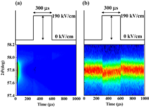
Fig. 1. Synchrotron XRD profiles around the diffraction peak of PZT 004 as a function of time when 190 kV/cm and 300 µs width rectangular pulse was applied with (a) conventional and (b) new setups.
Download figure:
Standard image High-resolution image3. Results and discussion
Figure 2 shows the XRD θ–2θ scan of the PZT film on the (100)cSrRuO3//(100)LaNiO3//(100)CaF2 substrate grown by pulsed-MOCVD. 00l reflection peaks from PZT were observed together with those from the substrate. The inset of Fig. 2 displays the X-ray pole figure measurement fixed at the 2θ angle corresponding to the {110} PZT diffraction peak. This X-ray pole figure measurement proved that the PZT film is epitaxially grown on the substrate. These results show that this PZT film consists of only a polar-axis (001)-oriented tetragonal phase. The estimated out-of-plane lattice parameter was 0.415 nm.
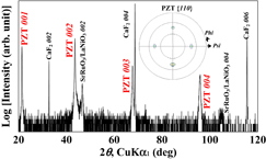
Fig. 2. XRD pattern and X-ray pole figure plot measured at fixed 2θ angle corresponding to PZT {110} diffraction peak for PZT film deposited on (100)cSrRuO3//(100)LaNiO3//(100)CaF2 substrate.
Download figure:
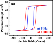
Standard image High-resolution imageFigure 3(a) shows the polarization–electric field (P–E) hysteresis loops measured using triangular waves of 5 and 1000 Hz. Well-saturated P–E hysteresis loops originating from the ferroelectricity were observed regardless of the applied electric field period. Saturation polarization (Psat) corresponds to the spontaneous polarization in this case because this film has a perfect polar-axis orientation. Psat of 65 µC/cm2 was found to be almost independent of the frequency at the electric field of 190 kV/cm. On the other hand, the coercive field (Ec) increased from 37 to 62 kV/cm with the increase in frequency from 5 to 1000 Hz. This was in agreement with the general trend of Pb(Zr,Ti)O3 films.31)
Download figure:
Standard image High-resolution image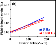
Fig. 3. (a) P–E hysteresis loops measured under a bipolar electric field and (b) S–E curves measured under a unipolar electric field period using triangular waves with 5 and 1000 Hz.
Download figure:
Standard image High-resolution imageFigure 3(b) shows the strain–electric field (S–E) curves measured under unipolar 5 and 1000 Hz triangular electric fields after the poling treatment. A linear response was observed in both cases. The field-induced strain was 0.06–0.08% at 190 kV/cm and the effective longitudinal piezoelectric coefficient d33(eff) estimated from Fig. 3(b) was approximately 36–45 pm/V. These results show that the piezoelectric response is almost independent of frequency.
Figure 4 shows the frequency dependences of the relative dielectric constant (εr) and dielectric loss (tan δ). εr was almost constant at approximately 200 in the 10 kHz–10 MHz frequency region, while tan δ was below 10%.

Fig. 4. Frequency dependences of the relative dielectric constant (εr) and dielectric loss (tan δ).
Download figure:
Standard image High-resolution imageFigure 5(a) shows the diffraction profiles as a function of time with applied pulse voltages of 0.3 µs width. Integrated synchrotron XRD θ–2θ patterns around the PZT 004 peak without voltage and under an applied electric field of 230 kV/cm are shown in Fig. 5(b). The diffraction peak shifted toward a lower angle with increasing applied voltage, which indicates the elongation of the crystal lattice along the electric field direction. Figure 5(c) shows the field-induced strain obtained from the peak shift data as a function of the applied electric field. An almost linear relationship across zero was obtained, suggesting the piezoelectric response of this film.

Fig. 5. (a) XRD diffraction profiles around the PZT 004 peak as a function of time with applied pulse voltages of 200 ns width and 230 kV/cm height. (b) Integrated diffraction θ–2θ patterns around the PZT 004 peak before and during electric field application and (c) field-induced strain as a function of applied electric field.
Download figure:
Standard image High-resolution imageFigure 6 shows the diffraction profiles around the PZT 004 peak as a function of time. Pulses of 190 kV/cm height and 0.3, 20, and 2000 µs widths were applied to the PZT film after the poling treatment at 230 kV/cm. A shift in peak position toward a lower angle by the applied electric field was clearly observed from the time-resolved XRD irrespective of the pulse time period. Integrated synchrotron XRD θ–2θ patterns around the PZT 004 peaks before, during, and after electric field application are respectively shown in Figs. 7(a)–7(c). The data obtained by applying a DC electric field is also shown in Fig. 7(d). The diffraction peaks shifted toward lower angles for all applied pulse widths only when the pulse voltages were applied, indicating the lattice elongation under the applied electric field. In addition, the positions of diffraction peaks obtained after electric field application are the same as those obtained before such application, indicating that the lattice elongation is a reversible phenomenon.
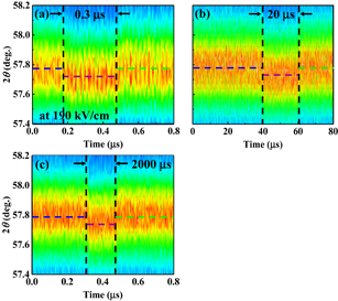
Fig. 6. Time-resolved XRD results for pulses of (a) 0.3, (b) 20, and (c) 2000 µs widths and 190 kV/cm height.
Download figure:
Standard image High-resolution image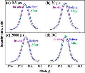
Fig. 7. (a–c) Integrated diffraction θ–2θ patterns around the PZT 004 peak before, during, and after electric field application obtained from the data shown in Figs. 6(a)–6(c). (d) Data obtained by applying DC electric field.
Download figure:
Standard image High-resolution imageThe pulse width dependence of the field-induced lattice strain can be estimated by comparing the diffraction peak shifts of the PZT film obtained before or after and during electric field application. Figure 8 shows the field-induced lattice strain as a function of frequency at 190 kV/cm calculated from the data shown in Fig. 7. No pulse width dependence of the field-induced lattice strain was verified in the range up to 1 MHz, which also the same as that of the applied DC. Moreover, the amount of field-induced lattice strain estimated from the time-resolved XRD results was almost the same as 0.06–0.08%, which corresponds to d33(eff) of approximately 36–45 pm/V, which is the same as those obtained from the S–E measurement shown in Fig. 3(b). The present result of the lattice elongation measured by time-resolved XRD is reasonable, taking into account the fact that the piezoelectric response originates from the lattice elongation induced by an electric field application in the present polar-axis-oriented tetragonal film. Furthermore, the frequency dependence of the effective electrostrictive coefficient Q33(eff) = d33(eff)/(2 × ε0 × εr × Pr), where ε0 is the dielectric constant in vacuum, is considered to be not very large because of the small frequency dependences of Pr, εr, and d33(eff) as respectively shown in Figs. 3, 4, and 8.

Fig. 8. Pulse width dependence of the field-induced strains calculated from time-resolved XRD measurement (circles) and PFM measurement (squares).
Download figure:
Standard image High-resolution image
Although the frequency dependence of the piezoelectric response has been investigated electrically and mechanically, there is no report on the direct frequency dependence measurement of the electric field response of the crystal lattice under an applied electric field. This experiment demonstrated the direct observation of the crystal structure change under an applied pulsed electric field by time-resolved XRD measurement for a wide frequency range that is useful for understanding the origin of the frequency dependence of the macroscopic piezoelectric properties. Although the present study measured the perfectly polar-axis-oriented tetragonal PZT film with only a lattice elongation contribution to the piezoelectric response, various contributions of the piezoelectric responses, such as phase change and domain switching, can be quantitatively evaluated as a function of frequency for the films including not only the 180° domain but also nonpolar orientations such as the 90° domain by the developed time-resolved XRD measurement method. These results are useful for understanding the frequency dependence of the piezoelectric response because the crystal structure change under an applied electric filed can be systematically investigated by changing the applied pulse width and repetition frequency. These results are also very useful for designing piezoelectric materials for devices under various frequencies.
4. Conclusions
We developed a setup for measuring the time response of the crystal structure change with various pulse widths under an applied electric field using a typical piezoelectric material of a 2.1-µm-thick epitaxial Pb(Zr0.5Ti0.5)O3 film with a perfect polar-axis orientation. Synchrotron X-ray was focused and irradiated on the Pt and pulses of 0.3 to 2000 µs width and 190 kV/cm height were applied to the PZT film. Lattice elongation was directly observed under an applied electric field and the lattice displacement estimated from the shift in diffraction peak position was almost constant at all pulse widths, indicating that strain did not depend on pulse width. The amount of field-induced lattice strain estimated by time-resolved XRD measurement was in good agreement with that calculated by S–E measurement.
Acknowledgement
This work was partially supported by JSPS KAKENHI Grant Numbers 15H04121, 26220907, and 16J10098. The synchrotron radiation experiments were performed at beamlines BL13XU of SPring-8 with the approval of the Japan Synchrotron Radiation Research Institute (JASRI) (Proposal No. 2016B1717).