
Abstract
(Bi1−xBax)FeO3 multiferroic thin films with ferromagnetism and ferroelectricity were fabricated by a pulsed DC reactive sputtering and applied to create a magnetic domain using an electric field. The (001)-oriented (Bi1−xBax)FeO3 thin films, the electric polarization direction of which is perpendicular to the film plane, were fabricated onto a non-single-crystalline substrate with a Ta seedlayer/(111)-oriented Pt underlayer. A low pulse frequency (long time for sputtering OFF) and a high sputtering power (high-energy deposition) were effective for the acceleration of the crystallization of the (Bi1−xBax)FeO3 phase owing to the enhancement of the surface diffusion of sputtered atoms on the substrate surface. The saturation magnetization of the film was approximately 90 emu/cm3 and the coercivity was approximately 2.5 kOe. Magnetic force microscopy analysis of the (Bi0.48Ba0.52)FeO3 film confirmed that the magnetization was generated by applying only a local electric field. The multiferroic film described here is expected to be useful for electric-field-driven magnetic devices.
Export citation and abstract BibTeX RIS
1. Introduction
Magnetization reversal by an electric field is a prospective technology for future magnetic devices owing to its low power consumption and easy operation for magnetization reversal. For example, in the case of magnetic recording devices such as hard-disk drives (HDDs), magnetic field writing will gradually become more difficult owing to the increase in the required magnetic field. This is because the switching magnetic field of recorded bits (coercivity of magnetic grains) increases to inhibit the thermal agitation of magnetization. Therefore, recently, energy-assisted magnetic recording technologies for next-generation HDDs such as thermally assisted magnetic recording1–3) and microwave-assisted magnetic recording4–6) have been widely studied to decrease the switching magnetic field. However, the energy-assisted magnetic recording technologies also consume large quantities of power and the structure of the magnetic field writing head is complicated owing to additional elements such as a plasmon antenna for thermally assisted magnetic recording or a spin torque oscillator for microwave assisted-magnetic recording. Therefore, a new technique for magnetization reversal is needed, and the electric field writing can be used for magnetic recording devices with multiferroic thin films. The power requirement for switching the magnetization direction by this process is very low, the structure of the writing element is simple (involving a needle-shaped conductive element), and a very high electric field can be easily applied to the multiferroic layer because it is thin.
Several techniques of controlling the magnetization by applying an electric field were reported. (1) The control of magnetization direction by applying an electric field was performed in piezoelectric and magnetostrictive laminate composites7,8) or multilayer structures.9,10) (2) The control of the magnetic anisotropy of a thin metallic magnetic layer by applying an electric field was performed in magnetic tunnel junctions with trilayers of thin metallic magnetic layer/thin insulating layer/metallic magnetic layer.11–13) (3) The reversal of the magnetization direction of a thin metallic magnetic layer by applying an electric field was performed in a bilayer with α-Cr2O3 (dielectric property and antiferromagnetic property)/thin magnetic layer.14,15) (4) The reversal of the magnetization direction of a thin metallic magnetic layer by applying an electric field was performed in a bilayer with BiFeO3 (high ferroelectric Curie temperature of 1120 K and high antiferromagnetic Néel temperature of 640 K)/thin magnetic layer.16–18) (5) The reversal of the magnetization directions of (Dy,Tb)FeO3,19) SmFeO3,20) and YbFeO321) (ferromagnetism and ferroelectricity at low temperature) by applying an electric field was performed. However, there are problems regarding magnetic device application in these systems. Complete magnetization reversal is difficult in system 1, both the electric field and the magnetic field are needed for magnetization reversal in systems 2 and 3, only a thin magnetic layer is effective for magnetization reversal in systems 2, 3, and 4, and only a very low temperature is effective for magnetization reversal in system 5. Therefore, a new system that can complete the magnetization reversal in a single phase (single layer) with ferromagnetism and ferroelectricity with a high Curie temperature is needed.
These days, suitable multiferroic materials such as (Bi1−xBax)FeO3,22) (Bi1−xBax)(Fe1−yTiy)O3,23) Ba(Ti1−xFex)O3,24) and Bi(Fe1−xCox)O325,26) with ferromagnetism and ferroelectricity at room temperature are reported. In a previous study, we fabricated Ta seedlayer/(111)-oriented Pt underlayer/(001)-oriented (Bi1−xBax)FeO3 multiferroic thin films with electric polarization perpendicular to the film plane onto a thermally oxidized Si wafer using an ultrahigh-vacuum (UHV) sputtering system.27) Very high frequency (VHF) (40.68 MHz) plasma irradiation with an electric power of 5 W was applied during the radio-frequency (RF) (13.56 MHz) sputter deposition28) of the (Bi1−xBax)FeO3 film. The (Bi0.6Ba0.4)FeO3 film, in which the Ba concentration was optimized, exhibited hysteresis curves indicating ferromagnetic and ferroelectric behavior and had a saturation magnetization of about 60 emu/cm3, a coercivity of about 2.5 kOe, and a high Curie temperature of about 400 °C. Magnetic force microscopy (MFM) analysis of the (Bi0.6Ba0.4)FeO3 film confirmed that the magnetization was reversed by applying only a local electric field.27) This indicates that the magnetization direction in the (Bi0.6Ba0.4)FeO3 film could be controlled on the micrometer scale by simply applying an electric field. However, the saturation magnetization and insulation of the films were insufficient for high-performance magnetic device application.
Here, a pulsed DC reactive sputtering technique was reported as a useful fabrication method of oxide or nitride films from the viewpoints of high deposition rate, high sputtering voltage, free arcs, and removal of charges on the surface of a sputtering target.29) Moreover, this fabrication method is also effective for the enhancement of the surface diffusion of sputtered atoms on the substrate surface by high-energy deposition with time interval. In this study, we fabricated high-qualified (Bi1−xBax)FeO3 thin films by reactive pulsed DC sputtering. We also demonstrated the control of the magnetization direction on the micrometer scale by applying a local electric field on a scanning probe microscope (SPM) with a Co–Zr–Nb-coated conductive tip.
2. Experimental methods
Multilayers of Ta (5 nm)/Pt (100 nm)/(Bi1−xBax)FeO3 (300 nm) were deposited onto a thermally oxidized Si wafer using a UHV sputtering system. The Ba concentration x was varied from 0.30 to 0.75. The Ta seedlayer, Pt underlayer, and (Bi1−xBax)FeO3 layer were deposited at room temperature, 300 °C, and 570 °C, respectively. The film thickness and deposition temperature of the Ta seedlayer and Pt underlayer were optimized to obtain a strong (111) orientation of the Pt underlayer.30) The VHF (40.68 MHz) plasma irradiation28) during the reactive pulsed DC sputtering deposition of (Bi1−xBax)FeO3 films was performed with an electric power of 5 W to obtain the crystal grain growth of (Bi1−xBax)FeO3 thin films. The frequency of pulsed DC was varied from 50 to 250 kHz. Here, the duty ratios between sputtering ON and OFF are about 2–3 and 1, for example, the time of sputtering ON is 15 µs and that of OFF is 5 µs for 50 kHz, and the time of sputtering ON is 2.6 µs and that of OFF is 1.4 µs for 250 kHz. The sputtering power of pulsed DC was varied from 100 to 200 W. The composition of the fabricated (Bi1−xBax)FeO3 films was analyzed by energy dispersive X-ray spectroscopy (EDS). The crystallographic orientations and crystalline structures of the fabricated (Bi1−xBax)FeO3 films were analyzed by X-ray diffraction (XRD) analysis. The magnetization curves of (Bi1−xBax)FeO3 films were measured using a vibrating sample magnetometer (VSM) with the application of a magnetic field parallel to the film surface. The ferroelectric hysteresis loops of the (Bi1−xBax)FeO3 films were measured using a ferroelectric tester. The local electric field was applied to the (Bi1−xBax)FeO3 film using an SPM with a conductive, magnetic Co–Zr–Nb tip. The electric and magnetic domain structures of the (Bi1−xBax)FeO3 film were analyzed by electric force microscopy (EFM) and magnetic force microscopy (MFM), respectively, with a conductive, magnetic Co–Zr–Nb tip.
3. Results and discussion
Figure 1 shows the XRD profiles of the Bi–Ba–Fe–O films fabricated with various Ba concentrations on a thermally oxidized Si substrate with a Ta/Pt layer. The profiles are differentiated by fabrication condition of pulsed DC frequency [(a) 250 kHz and (b) 50 kHz], because the pulsed DC frequency affects film quality, as described below. The Pt underlayer was found to have a strong (111) orientation and the full width at half maximum of the rocking curve for the Pt(111) diffraction was 2.0°. The Bi–Ba–Fe–O films with the Ba concentration of less than 0.55 were found to have a strong (006) peak; this indicates that these films have a (001) orientation. Here, the peak at around 35.8° is from the substrate, and the peak at around 37.2° is from the impurity phase or second phase (unknown phase) with a very small quantity. With increasing Ba concentration, the (006) peak shifts to a lower angle [Fig. 1(a)]. This indicates that the Bi atoms of the BiFeO3 phase are replaced by Ba atoms. On the other hand, in the case of Bi–Ba–Fe–O films with a Ba concentration of more than 0.6, the (006) peak disappears [Fig. 1(b)] and other peaks appear (not shown). This indicates that the formation of the BiFeO3 phase is hindered by an excess amount of Ba. These results indicate that the (Bi1−xBax)FeO3 films with x < 0.6 can be formed with a single phase.
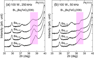
Fig. 1. XRD profiles of Ta seedlayer/Pt underlayer and Bi–Ba–Fe–O films on Ta/Pt layer fabricated with various Ba concentrations [pulsed DC frequencies of (a) 250 and (b) 50 kHz].
Download figure:
Standard image High-resolution imageFigure 2 shows the dependence of the saturation magnetization Ms on the Ba concentration in the Bi–Ba–Fe–O films fabricated by pulsed DC reactive sputtering. The dependence of Ms on the Ba concentration in the Bi–Ba–Fe–O films fabricated by RF sputtering is also shown for comparison in this figure. The sputtering power is changed in the case of Bi–Ba–Fe–O films fabricated by the pulsed DC reactive sputtering, and the sputtering power is optimized in the case of Bi–Ba–Fe–O films fabricated by RF sputtering. With increasing Ba concentration up to around 0.5, Ms increased in both Bi–Ba–Fe–O films fabricated by the pulsed DC reactive and RF sputterings. This is due to the transformation from the antiferromagnetic phase to the ferrimagnetic phase.22) The decrease in Ms in the Bi–Ba–Fe–O films with the Ba concentration of more than 0.6 is due to the inhibition of the formation of the (Bi1−xBax)FeO3 phase, as mentioned in Fig. 1. In the case of (Bi1−xBax)FeO3 films with the Ba concentration of about 0.5 fabricated by the pulsed DC reactive sputtering, Ms increases from 70 to 90 emu/cm3 with increasing sputtering power. The Ms of 90 emu/cm3 was 1.5 times larger than that of the (Bi1−xBax)FeO3 film with the Ba concentration of about 0.5 fabricated by the RF sputtering.
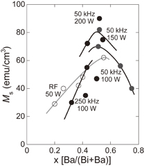
Fig. 2. Dependence of saturation magnetization on Ba concentration in Bi–Ba–Fe–O films fabricated by pulsed DC reactive sputtering with various fabrication conditions and RF sputtering.
Download figure:
Standard image High-resolution imageFigure 3 shows the in-plane magnetization curves (a), (c) and ferroelectric curves (b), (d) of the (Bi1−xBax)FeO3 (x ∼ 0.5) films fabricated by the pulsed DC reactive sputtering (a), (b) and RF sputtering (c), (d). A clear hysteresis loop in both magnetization and ferroelectric curves was observed. The Ms of the (Bi1−xBax)FeO3 film fabricated by the pulsed DC reactive sputtering was 1.5 times larger than that of the film fabricated by the RF sputtering, as mentioned before. The coercivity of magnetization curves was around 2 kOe, and the squareness S (= remanent magnetization Mr/Ms) was around 0.60. On the other hand, the coercivity and S with the out-of-plane direction of the film were 1.5 kOe and 0.40 (not shown), respectively. This indicates that this film has somewhat perpendicular magnetic anisotropy. These magnetic properties are available for magnetic devices. For the measurement of ferroelectric curves, the maximum electric field was about 200 kV/cm due to the insulating destruction. The hysteresis of the (Bi1−xBax)FeO3 film fabricated by the pulsed DC reactive sputtering was clearer than that of the film fabricated by the RF sputtering. The electric current at 5 V application for the (Bi1−xBax)FeO3 film fabricated by the pulsed DC reactive sputtering was 300 nA, which is 5 times smaller than that in the case of the RF sputtering. These indicate that the use of the pulsed DC reactive sputtering is the key to obtaining high-qualified (Bi1−xBax)FeO3 multiferroic films. The relationship between the magnetic and ferroelectric properties will be discussed in a future study because only the minor loop of the electric property was measured here.
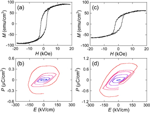
Fig. 3. Magnetization curves (a, c) and ferroelectric curves (b, d) of (Bi1−xBax)FeO3 (x ∼ 0.5) films fabricated by pulsed DC reactive sputtering (a, b) and RF sputtering (c, d).
Download figure:
Standard image High-resolution imageFigure 4 show the XRD profiles of the (Bi1−xBax)FeO3 (x ∼ 0.5) films fabricated by the pulsed DC reactive sputtering with various pulsed frequencies (a) and sputtering powers (b). As the pulsed frequencies are decreased and the sputtering powers are increased, the (Bi1−xBax)FeO3 (006) peak intensity increased. [This is considered to accelerate the crystallization of the (Bi1−xBax)FeO3 phase.] Figure 5 shows the dependences of Ms on the pulsed frequency (a) and sputtering power (b) in the (Bi1−xBax)FeO3 (x ∼ 0.5) films fabricated by the pulsed DC reactive sputtering. As the pulsed frequencies are decreased and the sputtering powers are increased, Ms increased. This is due to the acceleration of the crystallization, as mentioned in Fig. 4. (The reason for the acceleration of the crystallization is considered to be the enhancement of the surface diffusion of sputtered atoms on the substrate surface by high-energy deposition with a long time interval.)
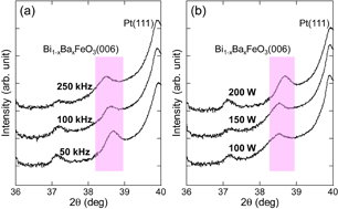
Fig. 4. XRD profiles of (Bi1−xBax)FeO3 (x ∼ 0.5) films fabricated by pulsed DC reactive sputtering with various pulsed frequencies (a) and sputtering powers (b).
Download figure:
Standard image High-resolution image
Fig. 5. Dependence of saturation magnetization on pulsed frequency (a) and sputtering power (b) in (Bi1−xBax)FeO3 (x ∼ 0.5) films fabricated by pulsed DC reactive sputtering.
Download figure:
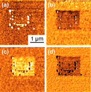
Standard image High-resolution imageFigures 6(a)–6(d) show topographic, MFM (tip end: N), EFM (tip end: +), and EFM (tip end: −) images, respectively, of the (Bi0.48Ba0.52)FeO3 film fabricated by the pulsed DC reactive sputtering with the pulsed frequency of 50 kHz and the sputtering power of 200 W after applying a DC voltage of −10 V (333 kV/cm) with 2 × 2 µm2 to the film. The MFM images were captured with a Co–Zr–Nb magnetic tip that was magnetized to saturation at the end of the tip such that the magnetization direction would be perpendicular to the sample surface and the direction of the detected magnetic field from the sample would also be vertical to the sample surface. For the EFM imaging, the Pt underlayer was grounded and a DC voltage of +1.0 V (+33 kV/cm) or −1.0 V (−33 kV/cm) was applied to the Co–Zr–Nb conductive tip. Because this DC electric field was smaller than the coercive electric field of the (Bi0.48Ba0.52)FeO3 film, as depicted in Fig. 3, polarization reversal did not occur during this imaging. In the MFM image obtained with the tip magnetized at the end, an attractive force between the tip and the sample was observed in the ferromagnetic domain structure, indicating that the magnetization direction was downward toward the film surface. In the EFM image obtained with the tip voltage of +1.0 V, a repulsive force between the tip and the sample was observed in the ferroelectric domain structure, which indicates a positive electric charge in this area. In an EFM image obtained with a tip voltage of −1.0 V, the attractive force between the tip and the sample was observed in the ferroelectric domain structure, which indicates a positive electric charge in this area. These images show that clear micrometer-scale ferroelectric domains were formed upon application of the local electric field. In an MFM image obtained with a tip voltage of 0 V, the attraction in the area and the surrounding area did not change for both before and after EFM measurements with tip voltages of −1.0 and +1.0 V (not shown here). Therefore, it can be concluded that micrometer-scale magnetization was achieved by applying a local electric field and that the directions of P and M are parallel. Thus, the proposed multiferroic films are expected to be useful in novel magnetic recording devices driven by electric field writing.
Fig. 6. (a) Topographic, (b) MFM (tip end: N), (c) EFM (tip end: +), and (d) EFM (tip end: −) images of (Bi0.48Ba0.52)FeO3 film after applying DC voltage of −10 V with 2 × 2 µm2 to the film.
Download figure:
Standard image High-resolution image
4. Conclusions
In this study, we fabricated high-qualified (Bi1−xBax)FeO3 multiferroic thin films by using pulsed DC reactive sputtering and demonstrated local magnetization reversal by the application of an electric field. The deposition with high energy with a long time interval is effective for the acceleration of the crystallization of the (Bi1−xBax)FeO3 phase owing to the enhancement of the surface diffusion of sputtered atoms on the substrate surface. The (Bi0.48Ba0.52)FeO3 film was found to have a high saturation magnetization of about 90 emu/cm3 and a high coercivity of about 2 kOe. MFM images revealed that the magnetization direction in the (Bi0.48Ba0.52)FeO3 film could be controlled on a micrometer scale by simply applying an electric field. From these results, the proposed multiferroic film is expected to be useful for applications in electric field-driven magnetic devices. We are developing equipment for the measurement of the electromagnetic effect (M–E curve) for multiferroic thin films. We will fabricate the multiferroic thin films with very high insulation and will complete the equipment for the measurement of the electromagnetic effect. Then, we will discuss the relationship between the magnetic and ferroelectric properties of the multiferroic thin films.
Acknowledgments
This work was partially supported by the Mazda Foundation, Casio Science Promotion Foundation, and JST/PRESTO (No. JPMJPR152C, ID: 15655293).
Biographies

Satoru Yoshimura received his Bachelor of Technology (Tohoku University, 1998), Master of Technology (Tohoku University, 1999), and Doctor of Technology (Tohoku University, 2002) degrees. He became a JSPS Research Fellow at the Graduate School of Engineering, Tohoku University (2001), a Research Associate at the Graduate School of Engineering, Nagoya University (2005), an Assistant Professor at the Graduate School of Information Science and Electrical Engineering, Kyushu University (2007), an Associate Professor at the Research Center for Engineering Science, Akita University (2008), and a PRESTO Researcher of JST Strategic Basic Research Programs (2015). His research focuses on the development of electric field-driven magnetic devices with highly functional magnetic thin films.

Munusamy Kuppan received his Bachelor of Science (Thiruvalluvar University, 2007), Master of Science (Thiruvalluvar University, 2009), Master of Philosophy (University of Madras, 2011), and Doctor of Philosophy (VIT University, 2015) degrees. He became a Research Assistant at the Centre for Crystal Growth, VIT University (2016), and a Postdoctoral fellow at the Regional Innovation Center, Akita University (2017). His research focuses on the search and fabrication of highly functional magnetic thin films and their applications.