
Abstract
LiNbO3 (LNO) is currently intensively studied as an important ferroelectric material. In this work, polycrystalline LNO films were prepared through a sputtering technique, and their ferroelectricity-related resistive switching property was investigated using a device structure of PtSi/SiO2/LNO/Pt. The device exhibits a volatile resistance switching property at lower positive sweeping voltages and a stable bipolar nonvolatile switching property at higher sweeping voltages. The resistive switching mechanism of the device is discussed based on the domain wall conductivity characteristics of the polycrystalline LNO thin films. The PtSi/SiO2/LNO/Pt memristor device has potential applications in memory and artificial neural synapses.
Export citation and abstract BibTeX RIS

Content from this work may be used under the terms of the Creative Commons Attribution 4.0 license. Any further distribution of this work must maintain attribution to the author(s) and the title of the work, journal citation and DOI.
Strong spontaneous polarization is a typical property of ferroelectric materials. When ferroelectric domains are oriented differently, domain walls (DWs) form between them. The discontinuity of polarization strength components perpendicular to DWs results in the accumulation of bound charges at the DWs, contributing to local electric conductivity. This phenomenon is called domain wall conductivity (DWC). 1–4) DWC in ferroelectric materials is determined by the type and density of the bound charge and is related to the inclination angle and polarization strengths of the domains on both sides. 4–8)
In the case of bulk ferroelectric materials, which are usually thicker than 100 μm, domains can be stably formed and controlled by the applied bias. However, the high coercive voltage required by the coercive field, as large as 2.1 × 10⁵ V/cm, 9) significantly limits the bulk ferroelectric materials in DWC applications. As the thickness is reduced to several hundred nanometers in ferroelectric films, the coercive voltage is significantly reduced. For example, a 16 V coercive voltage was observed in a 200 nm film of LiNbO3 (LNO). 10) In various ferroelectric devices such as supercapacitors and tunnel junctions, ferroelectric films are contacted with metal electrodes. As the polarization within the ferroelectric thin film is interrupted at the metal/ferroelectric interface, interfacial bound charges are generated. In early studies, the Thomas–Fermi theory was proposed to address the electrostatic potential problem at the metal/ferroelectric interface. 11–13) According to the theory, the ability of a metal to shield the electric field generated by the bound charges depends on the metal's Fermi level and electron density. This shielding ability is described by the metal's screening length. A smaller screening length of the contacting metal ensures full shielding of the interfacial bound charges. However, for metals with a large screening length, the compensation charges in the metal are less than the bound charges. As a result, a non-vanishing electric field opposite to the polarization is built inside the ferroelectric film, which is called the depolarization field. Under the depolarization field, the surface polarization direction can be reversed to form a surface reversion layer in the ferroelectric film. 5,12–15)
In recent years, LNO has been intensively investigated as an important ferroelectric material owing to its high spontaneous polarization of 0.70 C m−2 and high Curie temperature of 1210 °C. 16–18) The DWC property has been intensively studied in single-crystal LNO films for the preparation of memristors. 8,10,19) An on/off ratio as high as 1012 has been reached by the single-crystal LNO memristor. 20) In other studies on ion-exfoliated single-crystal LNO films, oxygen vacancy-based filaments were also reported to result in resistive switching properties. 21–23) On the other hand, the possible DWC-related resistive switching properties in polycrystalline LNO (poly-LNO) films have rarely been studied. Compared with single-crystal LNO, poly-LNO has the merit of easy fabrication.
In this research, poly-LNO films were fabricated via magnetron sputtering and subsequent thermal annealing. The phenomenon of low resistance state in poly-LNO in a double inert electrode PtSi/LNO/Pt device was observed. With the introduction of SiO2, a device of PtSi/SiO2/LNO/Pt was proposed to realize resistive switching characteristics based on DWC.
To study the ferroelectric property of the LNO films, LNO was prepared via magnetron sputtering on PtSi electrode substrates at room temperature. The PtSi electrode substrate was prepared through the sputtering of 150 nm Pt on the Si (100) substrate followed by rapid thermal annealing (RTA). The purity of the Pt target was 99.99%. The annealing was conducted at 800 °C for 1 min in air or in pure nitrogen environment (99.999%). After annealing in pure nitrogen environment, the formed 300 nm thick PtSi layer exhibited a sheet resistance of 0.39 Ω/□ with high thermal stability. In another way, the PtSi bottom electrode was formed through annealing in ambient air. Due to the oxidation effect, a surface SiO2 layer is naturally formed on top of the PtSi. Before LNO sputtering, the base pressure of the vacuum chamber was pumped to 1 × 10⁻⁴ Pa and the working pressure was raised to 0.5 Pa by Ar gas flow (99.999%). The sputtering radio frequency power was controlled at 180 W and the deposition time was 1054 s. The as-deposited LNO films were amorphous. To form poly-LNO, the as-deposited LNO film was subjected to RTA in air at 800 °C for 20 min. Finally, 150 nm thick top Pt electrodes with a diameter of 800 μm were sputtered onto the annealed LNO films through a mechanical mask. This completed the test device structure of PtSi/LNO/Pt (from bottom to top) or the memristor device structure of PtSi/SiO2/LNO/Pt depending on the annealing condition of the bottom PtSi electrode. The property of the PtSi/LNO/Pt device was measured for comparison.
The morphological, crystalline, and ferroelectric properties of the poly-LNO films were characterized via scanning electron microscopy (SEM, Sigma HD VP SEM, Zeiss, Germany), X-ray diffraction (XRD, Ultima-IV, Rigaku, Japan), and piezoresponse force microscopy (PFM, Cypher-S, Asylum Research, United States). The morphology of the sample was characterized via atomic force microscopy (AFM, Cypher-S, Asylum Research, United States) for comparison with the PFM. The resistive switching behavior of the poly-LNO devices was measured using a Keithley 2611B sourcemeter controlled by a LabVIEW testing program. The devices were subjected to both single voltage sweeps and cycling loops.
The SEM images in Figs. 1(a) and 1(b) show the surface morphologies of the LNO films before and after RTA at 800 °C, respectively. Cross-sectional images are presented as insets. The thicknesses of the sputtered LNO films were measured as 120 nm and the surfaces of the films subjected to RTA at 800 °C exhibited grain-like appearances. The diameter of the grains ranged from 200 to 300 nm. Figure 1(c) shows the XRD patterns of the LNO films on the PtSi electrode layer. Before annealing, LNO films were amorphous. After RTA at 800 °C, diffraction peaks from the LNO (012), (104), (110), and (006) crystal planes occurred at 2θ positions of 23.76°, 32.76°, 34.84°, and 38.9°. The sharp (006) peak at 39.08° indicated a preferred c-axis growth orientation of the LNO films. The c-axis was the spontaneous polarization direction of the LNO ferroelectric domains.

Fig. 1. (a), (b) SEM surface morphology of the as-deposited LNO film on the PtSi layer before and after RTA at 800 °C. The corresponding cross-sectional views are presented as insets. (c) XRD patterns of the above LNO films, in comparison with the standard PDF card of LNO. (d), (e), (f) AFM morphology, PFM amplitude, and PFM phase of the 120 nm poly-LNO film on PtSi. (g) Phase-hysteresis loop of the poly-LNO film. (h) Domain writing on the poly-LNO film.
Download figure:
Standard image High-resolution imageThe ferroelectric properties of the LNO films before and after 800 °C annealing were characterized via vertical PFM. During PFM scanning, the bottom PtSi electrode was grounded. For the unannealed LNO, PFM yielded no signal (not shown). Therefore, the amorphous LNO film did not exhibit any ferroelectric properties. The PFM amplitude and phase diagrams after 800 °C annealing are shown in Figs. 1(e) and 1(f), and the surface grain-like AFM morphology is shown in Fig. 1(d). The PFM domain mapping exhibited a similar contour to the AFM grain distribution. Consequently, the DWs were well situated within the grain boundaries. Thus, the domains also exhibited a size distribution of 200–300 nm. Figure 1(g) depicts a typical phase-hysteresis loop of the poly-LNO films. Positive coercive voltage (Vc+) and negative coercive voltage (Vc−) of 10 V and −10 V were obtained. The value of the coercive voltage was comparable to the 16 V and −16 V Vc previously observed for a 200 nm single-crystal LNO film, 10) indicating that no significant difference in coercive voltages occurred between single-crystal LNO and poly-LNO films. Figure 1(h) depicts the ferroelectric PFM domain-writing operation on the poly-LNO film. Polarization voltages of +30 V and −30 V were separately applied to the upper and lower halves of the square scanning region. After writing, downward polarization in the upper half and upward polarization in the lower half were observed. However, dark stripes in the upper half and bright stripes in the lower half were also observed. These anomalous polarization areas were all located along the film grain boundaries. This phenomenon was rarely observed in experiments on single-crystal LNO. The phenomenon is attributable to the high density of defects at the grain boundaries of the poly-LNO films. 24,25)
In the PtSi/LNO/Pt device, The I–V test structure is shown in Fig. 2(a). Figure 2(b) shows that the as-deposited amorphous LNO film exhibited high resistance, which demonstrating the insulating nature of LNO. However, after 800 °C annealing, the poly-LNO film exhibited a significant reduction in resistance, as shown in Fig. 2(c). According to the above ferroelectric domain property study on the poly-LNO film, the reduction of the resistance can be ascribed to DWC. Since the film's thickness was only 120 nm and the ferroelectric domains having an average size of 200–300 nm, the grain boundaries or the DWs easily connected the top and bottom electrodes, providing possible current paths. The measured low-resistance state (LRS) was as low as ∼100 Ω. According to a method developed by Radmir Gainutdinov, 26) a revised formula is provided below.

where RDW denotes the total DWC resistance; w denotes the total width of the DWs; t denotes the DW thickness, which is assumed to be ∼20 nm; 8,26) L denotes the length of the DW that can be roughly replaced by the thickness of the poly-LNO film. Taking the grain boundaries as the DWs, according to the measured LRS of ∼100 Ω, the DWC was estimated as 1.2 × 10⁻³ (Ω•cm)−1, which is comparable to that estimated for single-crystal LNO films. 27) Therefore, the LRS hereafter is referred to "DWC LRS." Within the scanning voltage range of −3 V to 3 V, the DWC LRS remained unchanged owing to the small voltage magnitude, which is considerably smaller than the coercive voltage Vc.

Fig. 2. (a) Schematic of the PtSi/LNO/Pt test structure for LNO film conductance. The diameter of the top Pt electrode is 800 μm. (b), (c) I–V curves of LNO films before and after RTA-800 °C.
Download figure:
Standard image High-resolution imageIn the above test, DWC led to the LRS of the poly-LNO films. To fabricate devices with resistive switching capability, a high-resistance state (HRS) needs to be introduced. According to the Thomas–Fermi screening theory, it is assumed that an electrode with lower screening ability can generate a surface layer of domain reversal in the domains. Jiang et al. observed that the surface domain reversal layer provided resistive switching properties. 10,28,29) To enlarge the screening length of the electrode in our device, a SiO2 layer is to be intercalated to modify the electrical property of the PtSi/LNO/Pt device.
In the aforementioned bottom electrode fabrication process, we also prepared the PtSi bottom electrode through annealing in air. The annealing of the 150 nm-thick Pt on Si (100) in air at 800 °C for 1 min resulted in the formation of a surface SiO2 layer with a thickness of 45 nm. The sheet resistance of the total PtSi/SiO2 films was increased to 0.8 Ω/□ owing to the oxidation effect. Based on the PtSi/SiO2 stack films, a device structure of was finally fabricated by the following deposition of the poly-LNO film and the top electrode Pt (Fig. 3). To study the individual electrical properties of the SiO2 layer produced by annealing in air, a device structure of PtSi/SiO2/Pt was formed by a following Pt electrode deposition. It was found that the SiO2 layer was leaky in the vertical direction, showing a resistance of several ohms, and no resistive switching behavior was observed. Therefore, the series resistance contributed by the SiO2 layer can be neglected in the following study on the resistive switching property of the PtSi/SiO2/LNO/Pt device.

Fig. 3. Cross-sectional SEM image of the PtSi/SiO2/LNO/Pt device.
Download figure:
Standard image High-resolution imageFigure 4(a) depicts the schematic of the prepared PtSi/SiO2/LNO/Pt device. During the following electrical measurements, a positive voltage sweep was applied to the top Pt electrode, with the bottom PtSi electrode grounded. As the applied voltage was swept from 0.62 V to 1.10 V, the initial DWC LRS with a resistance rapidly switched to an HRS, as shown in Fig. 4(b). As the voltage decreased from 3 V to 0 V, the HRS switched back to LRS. This operation could be repeatedly performed in the following positive voltage-sweeping cycles. The above HRS/LRS switching under positive bias showed a volatile property. During the above sweepings, a threshold voltage (Vt) can be defined. Vt refers to the transition voltage range within which LRS and HRS are switched. For the negative voltage sweepings shown in Fig. 4(c), the device was initially in an LRS. As the voltage was swept from −0.52 V to −1.10 V, the device switched from LRS to HRS, corresponding to a negative Vt (−Vt). However, as the voltage was swept back from −5 V to 0 V, the device remained in its HRS. Even when the negative bias was repeatedly swept, the HRS of the device was found to be stable. All of the above sweepings had an average scanning speed of 0.5 V s−1.
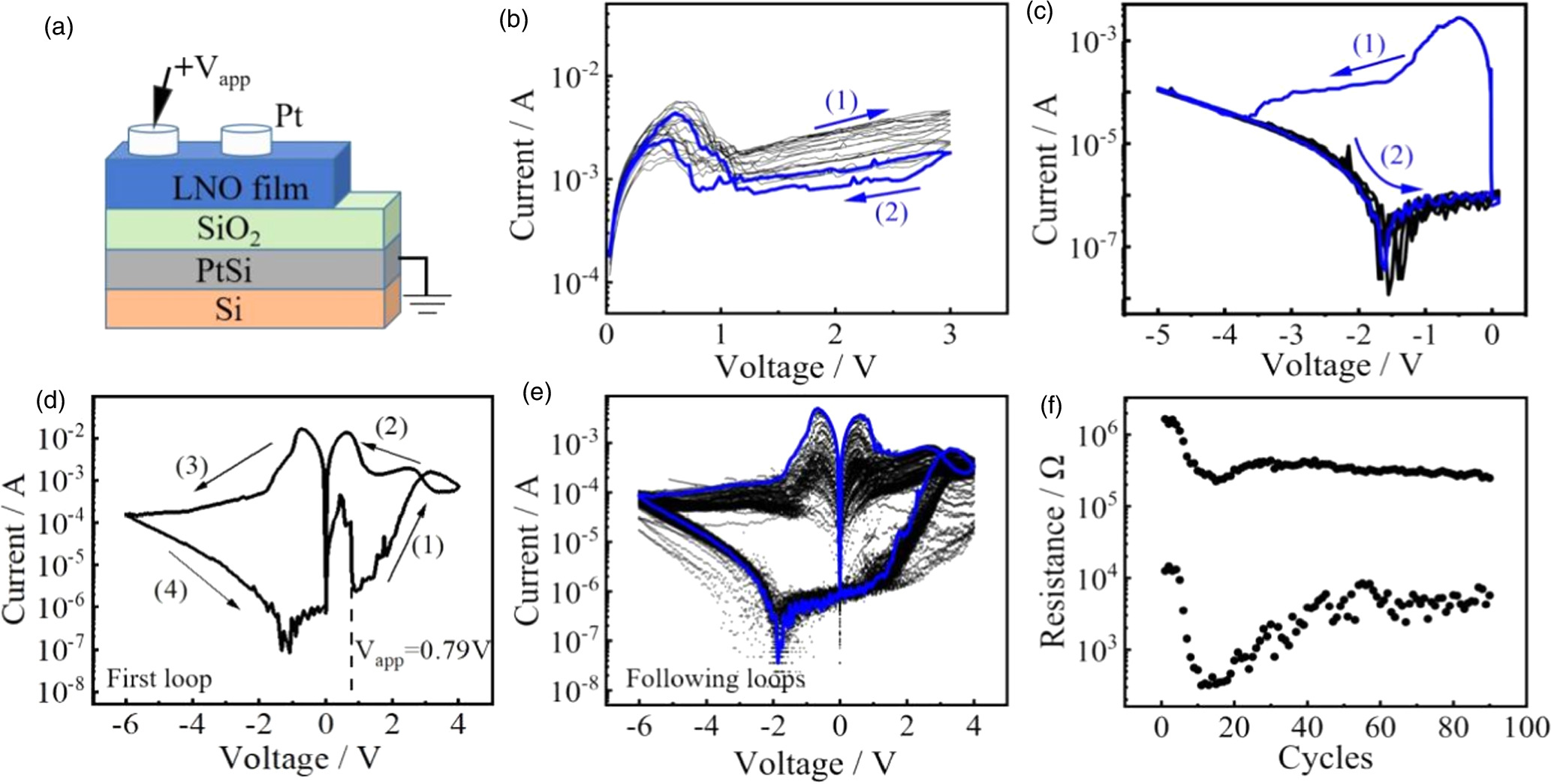
Fig. 4. (a) Schematic of the PtSi/SiO2/LNO/Pt device. (b) I–V curves of positive sweeping cycles between 0 V and 3 V. (c) I–V curves of negative sweeping cycles between 0 V and −5 V. (d) I−V curve of the first full-range loop of 0 V→4 V→0 V→–6 V→0 V. (e) I–V curves of the following 90 full-range loops. (f) Extracted HRS and LRS resistances from the 90 loops, estimated at a bias of −0.36 V.
Download figure:
Standard image High-resolution imageFigure 4(d) shows the result of the first sweeping loop when a full-range sweeping loop of 0 V→4 V→0 V→−6 V→0 V with a much faster sweeping speed of ∼3.0 V s−1 was applied to the device. The Vt value was approximately 0.56 V to 0.79 V, and −Vt was approximately −0.60 V to −1.68 V. Moreover, as the device entered the HRS during the negative voltage sweep, it did not return to the LRS until the end of the first loop. The resistance of the HRS was ∼105 Ω in the sweeping bias range from −2 V to 0 V. To switch back from this HRS to an LRS, applying a higher positive voltage sweep proved effective. The following 90 full-range loops are shown in Fig. 4(e), which showed bipolar resistive switching property. The HRS could be repeatedly switched back to the LRS upon the completion of a positive voltage sweep of 0 V→4 V→0 V. The resistances corresponding to the HRS and LRS of the 90 cycles are depicted in Fig. 4(f). They were recorded at a bias of −0.36 V. The switching on/off ratios ranged from 10 to 103.
According to the Thomas–Fermi screening theory, the SiO2 layer weakened the electric shielding ability of PtSi. Therefore, a depolarization field and a domain inversion layer were expected to form at the bottom surface of the LNO domains. The grain domains were then separated into bulk regions (b-region) and interfacial inversion regions (i-region), as depicted in Fig. 5(a). For clarity, only two c-axis polarization domains are shown. The ferroelectric polarity of the b-regions remained stable unless the applied biases exceeded Vc. The ferroelectric properties of the b-regions significantly contributed to the overall domain properties, as detected via PFM. However, in the i-regions, the naturally formed domain inversion layer easily adjusted its polarity in response to the applied bias. In an equilibrium state with zero bias or under weak bias, the i-regions retained their reversed polarity. The DWs could still make contact with the bottom electrodes, ensuring the DWC LRS of the device. When the bias exceeded Vt, the i-regions adjusted their polarities to align with the applied electric field. 10) According to a previous study, 2) the conductivity of the DW is highly dependent on the relative polarization directions of the adjacent pair domains. An alignment of the pair domains can cause reduced conductivity of the DWs. Therefore, the alignment of the polarity directions in the i-regions under a high bias contributed to the HRS of the device, as depicted in Fig. 5(b). When the positively applied voltage dropped below Vt, the domain reversal layers reverted to their initial polarity orientations owing to the inherent depolarization field, restoring the DWC, as depicted in Fig. 5(c). This completed the positive-voltage first half of the full-range loop.

Fig. 5. Device workflow diagram, domains (arrows), and DWs (grey dotted lines). (a)–(e) Application of varied voltages induces alterations in DWs, resulting in consequential effects on the device's on/off state.
Download figure:
Standard image High-resolution image
When the following negative voltage sweep was applied, a negative Vt (−Vt) was expected. However, as the device was transitioned into the HRS by a large negative bias, it did not easily return to the LRS upon the removal of the negative bias. In other words, −Vt was effective only for LRS–HRS switching but ineffective for HRS–LRS switching. This resulted in a non-volatile memory effect. This phenomenon was related to the intercalated SiO2 layer. Studies on SiO2 films have shown that oxygen vacancies in SiO2 can easily capture the positive-charged holes and the trapped holes can be neutralized or restored through the application of voltage biases in a metal–insulator–metal structure. 30,31) Therefore, in our PtSi/SiO2/LNO/Pt device, the positive charges were stored in the SiO2 layer upon the application of a large negative bias, as depicted in Fig. 5(d). Upon the withdrawal of the negative bias, the remaining trapped positive charges continued to control the polarization direction of the i-region through the electric field, as depicted in Fig. 5(e). Thus, the HRS of the device was reserved. In the next sweeping loop, as a high positive bias was applied to the device, the trapped holes were released from the SiO2 layer [Fig. 5, from (e) to (b)]. The device regained the ability to switch back to the LRS. So the mechanism of the above nonvolatile resistive switching is based on the tuning of the DWC in the i-region of the poly-LNO domains, which is controlled by the SiO2 layer and the applied biases.
To verify the function of the intercalated SiO2 layer on the DWC resistive switching of the device, a sputtering-deposited SiO2 layer with the same thicknesses of 45 nm was prepared to replace the oxidized SiO2 layer. The fabricated device had the same structure as PtSi/SiO2/LNO/Pt and also showed a bipolar resistive switching property, which is similar to the sweeping I–V curves shown in Fig. 4(e).
DWC enabled resistive switching under low voltage sweeping loops from −6 V to 4 V. All the voltages are lower than the coercive voltages of 10 V and −10 V. Therefore, the DWC resistive switching in this study did not alter the polarization orientation of domain bulks in the LNO films. Such alteration would require voltage biases higher than the coercive voltage. Instead, HRS/LRS switching was achieved through control over the surface reversal layers based on low-voltage sweeping. This research has inspiring implications for the application of poly-LNO films in information storage and synaptic devices.
In conclusion, experiments revealed that crystal grains formed in sputtered poly-LNO films on a PtSi electrode were closely related to polarized domains. Therefore, the grain boundaries can be regarded as DWs. The PtSi/SiO2/LNO/Pt device exhibited a volatile resistive switching property under a positive voltage sweepings from 0 V to 3 V. And the non-volatile bipolar resistive switching characteristics were observed under sweeping loops from –6 V to 4 V. Both properties are ascribed to the DWC tuning of the poly-LNO film. The low cost and low power consumption of DWC resistive switching in poly-LNO endow the device with greater application versatility.
Acknowledgments
We are grateful to Senior Engineer Yibo Zeng at the Pen-Tung Sah Institute of Micro-Nano Science and Technology for assistance on PFM testing and for the helpful comments.