
Abstract
Strained-Si technology is crucial to improving the performance of metal-oxide-semiconductor field-effect transistors (MOSFETs). To introduce large strain into the channel, we proposed a structure for the negative thermal expansion gate electrode. In this study, we used manganese nitride as the gate material, which is a negative thermal expansion material. The fabricated MOSFETs with the manganese nitride gate showed a 10% increase in electron mobility compared to the MOSFET with the Al gate. The results show that the negative thermal expansion gate technology is promising as a technology booster for MOSFET scaling.
Export citation and abstract BibTeX RIS

Content from this work may be used under the terms of the Creative Commons Attribution 4.0 license. Any further distribution of this work must maintain attribution to the author(s) and the title of the work, journal citation and DOI.
To enhance the carrier mobility in metal-oxide-semiconductor field-effect transistors (MOSFETs), various strain introduction technologies have been studied. 1–3) Well-known examples are the application of SiN stress liner and SiGe-source/drain structure as strain technologies. 4–7) As a result of these advancements, MOSFETs' scaling has been improved. Recently, other strain technologies have been strongly required for further scaling down of MOSFETs. This study proposes the use of negative thermal expansion materials as gate electrodes to introduce larger strain into the channel of MOSFETs. The conclusion section summarizes the important results and impact of the research.
Generally, the volume of the materials expands when the temperature of the materials increases. However, a limited number of compounds indicate negative thermal expansion. 8–16) Here, negative thermal expansion indicates that the volume of the materials shrinks when the temperature of the materials increases. Advanced ICs have various stress/strain issues that could be resolved by the negative thermal expansion materials. 17–21) The unique characteristics of negative thermal expansion materials have been considered for application in semiconductor packaging, microelectromechanical systems, and superconductivity. 22–24)
The coefficient of thermal expansion (CTE) mismatch between different materials is a principal factor that induces film stress. In advanced MOSFETs, the strain is introduced into the channel material because of the film stress induced by the CTE mismatch. Therefore, a large CTE mismatch can introduce a large strain into channel materials. 25,26) The CTE mismatch between the gate electrode and substrate also introduces strain into the channel material. TiN, which is usually used as the gate electrode, has a higher positive CTE than that of Si. Thus, a thicker TiN layer increases the strain of a Si channel along the compressive direction. 27) Therefore, negative thermal expansion materials have significant prospects by the introduction of tensile strain into MOSFET channels.
Figure 1 shows the conceptual drawing of the MOSFET with a negative thermal expansion gate electrode for carrier mobility enhancement. Generally, the deposition process of gate electrode material, such as sputtering and chemical vapor deposition, is performed at a high temperature. In addition, the post-annealing process is often required after deposition to improve crystallinity. These facts indicate that temperature lowering always occurs for gate formation. If the gate electrode material has a negative CTE, the temperature lowering expands the volume of the gate electrode. Thus, negative thermal expansion can introduce tensile strain into the channel material of the MOSFETs. The tensile strain induced by the negative thermal expansion gate electrode can enhance electron mobility. The use of negative thermal expansion materials as gate electrodes to introduce strain is a unique and unprecedented approach.

Fig. 1. (Color online) Conceptual drawing of the introduction of tensile strain into the MOSFET using the negative thermal expansion gate electrode.
Download figure:
Standard image High-resolution imageIn this study, we fabricated and evaluated nMOSFETs with negative thermal expansion gate electrodes. Subsequently, we first demonstrated the ability of the negative thermal expansion gate electrode to enhance electron mobility in nMOSFETs.
To introduce a large strain in the channel of the MOSFETs, we focused on an antiperovskite manganese nitride compound that exhibits negative thermal expansion. Manganese nitride compounds with an antiperovskite crystal structure are unique materials with several characteristics, such as a near-zero temperature-coefficient of resistivity and magnetocaloric effects. 28–31) The absolute value of the CTE of manganese nitride compounds is extremely high compared with that of other materials with negative CTEs. 12–16) Meanwhile, the Young's modulus of manganese nitride compounds exceeds 200 GPa, 32) which is sufficient to introduce a large strain. In addition, the resistivity of the manganese nitride compounds is approximately 300 μΩcm, which is almost the same as the resistivity of the doped poly-Si. 31,33) Moreover, manganese nitride compounds behave like metals rather than semiconductors. 31) Thus, the depletion layer is not formed in the gate electrode when the manganese nitride is used as a gate electrode material. Therefore, an antiperovskite manganese nitride compound is a promising material for gate electrodes to enhance electron mobility in MOSFETs.
First, we measured the X-ray diffraction (XRD) characteristics of the manganese nitride thin film deposited by radio-frequency magnetron sputtering to validate the negative thermal expansion. Figure 2(a) shows the XRD spectrum of the manganese nitride thin film deposited on the Si wafer. The thickness of the manganese nitride thin film was 200 nm. The power, the pressure, and the gas of the sputtering were 50 W, 0.5 Pa, and Ar, respectively. Using the dopant for the antiperovskite manganese, the CTE value and the temperature region can be controlled, which shows a negative CTE. Here, we used Sn and Zn as the dopant materials. The compositional ratio between Sn and Zn was 1:2. The XRD spectrum of the manganese nitride thin film was measured at temperatures of 30 °C, 50 °C, and 70 °C. The measurements were performed under high temperatures and then under low temperatures. We confirmed the peak position and intensity ratio of the fabricated sample to be similar to that of the antiperovskite manganese nitride compounds. 12,34,35) Furthermore, we obtained the change ratio of lattice spacing from the XRD peak positions, as shown in Fig. 2(b). We validated that fabricated manganese nitride thin film shrunk with an increase in temperature. Therefore, it is demonstrated that fabricated manganese nitride thin films have a negative CTE around room temperature. Additionally, this manganese nitride thin film can be used as a gate electrode that induces tensile stress around room temperature. We fabricated the MOSFETs using this manganese nitride thin film as the gate electrode material.
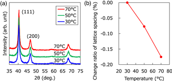
Fig. 2. (Color online) (a) XRD spectra of the manganese nitride thin film measured at 30 °C and 70 °C, and (b) Change ratio of lattice spacing obtained from XRD spectra.
Download figure:
Standard image High-resolution imageFigure 3(a) illustrates the process flow and the photograph of the fabricated nMOSFET with the manganese nitride gate. After the isolation process, we performed channel implantation. Subsequently, source/drain implantation was performed with the dummy gates. The dopant for the source/drain was arsenic of 1 × 1020 cm−3. Then, the rapid thermal annealing process was performed at the temperature of 1050 °C for 10 s for source/drain activation. We used Al with 0.5% Si and 0.5% Cu for the source/drain electrode and metal line. After that, we formed the manganese nitride gates. The thickness of the manganese nitride gate and the gate oxide were 200 nm and 10 nm, respectively. The gate oxide was SiO2, formed before the metal line process by thermal oxidation. Radio-frequency magnetron sputtering was also used as the deposition method of the manganese nitride gates, which was the same as that of the samples used for XRD analysis. Finally, the samples were annealed at 100 °C under a pressure of 10 Pa with an Ar atmosphere to obtain the tensile strain, as illustrated in Fig. 1. Here, we used a silicon-on-insulator substrate whose layer thickness was 100 nm. MOSFETs with an Al gate were also fabricated using the same process for comparison.
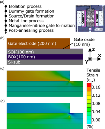
Fig. 3. (Color online) (a) Process flow and photograph of the fabricated nMOSFET with the manganese nitride gate electrode, (b) structure used in FEM simulation, (c) simulation results of the strain distributions in the MOSFETs with Al gate electrode, and (d) manganese nitride gate electrode.
Download figure:
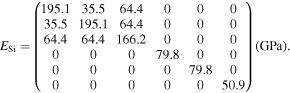
Standard image High-resolution imageSubsequently, we estimated the strain induced by the manganese nitride gate by finite element method (FEM) simulation. Figure 3(b) shows a cross-section of the structure used in the FEM simulation, which was the same as the structure of fabricated MOSFETs. The current flow was along the x-direction in the figure. The CTE of Si, SiO2, and Al were 2.46 ppm, 0.45 ppm, and 23.0 ppm, respectively. The CTE of the manganese nitride was the value obtained from the XRD measurements. The Young's modulus of SiO2, Al, and the manganese nitride were 73 GPa, 71 Gpa, and 200 GPa, respectively. In contrast, it is well-known that a single crystalline Si has an anisotropic Young's modulus. In this study, we used an Si wafer having (100) surface and (110) orientation flat. Thus, we used the following stiffness matrix (ESi) as the Young's modulus of Si to consider the effect of the current direction on the crystal orientation of the Si wafer. 19)
Here, the current direction was perpendicular to the (110) plane. The structure was subjected to the same thermal process succeeding gate formation as illustrated in Fig. 3(a).
Figures 3(c) and 3(d) show the FEM simulation results of the strain distribution in the MOSFETs with Al and the manganese nitride gate at 25 °C. The results illustrate the normal strain in the current direction (εxx). The Young's modulus of Al was lower than that of Si, and the CTE of SiO2, which is the gate oxide, was much lower than that of Al. Thus, little tensile strain was impressed on the Si channel of the MOSFET with Al gate. In contrast, we observed a high tensile strain of approximately 0.06% in the Si channel of the MOSFET with the manganese nitride gate having a negative CTE. These FEM simulation results indicated that tensile strain was induced in the Si channel by the negative CTE gate.
We also measured the current–voltage and mobility characteristics of the fabricated MOSFETs with a manganese nitride gate to confirm whether the manganese nitride could work as the gate electrode. Figures 4(a) and 4(b) show the drain current–gate voltage (ID–VG) and current–drain voltage (ID–VD) characteristics of the fabricated nMOSFETs. The gate length and width of the measured nMOSFET were 10 μm. The ID–VG characteristics were measured under drain voltages of 0.05 and 2.0 V. The ID–VD characteristics were measured under gate voltages of 0.2–2.0 V in increments of 0.2 V. The fabricated nMOSFETs with manganese nitride gates exhibited typical characteristics. These results indicate that the manganese nitride can work as the gate electrode of the MOSFET. In the negative gate voltage region, the drain current under the drain voltage of 2.0 V increased compared with the drain current under the drain voltage of 0.05 V. We consider that the drain current under the negative gate voltage is mainly composed of gate-induced drain leakage in the case of the fabricated devices. Therefore, the drain current under the negative gate voltage increased as the drain voltage increased.
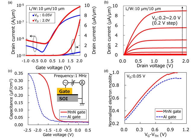
Fig. 4. (Color online) (a) ID–VG, and (b) ID–VD characteristics of the fabricated nMOSFET with a manganese nitride gate. (c) Comparison between the manganese nitride gate and Al gate through the C–V characteristics and (d) the electron mobility characteristics.
Download figure:
Standard image High-resolution imageFigure 4(c) illustrates the capacitance–voltage (C–V) characteristics of the fabricated MOSFETs with manganese nitride and Al gates. The measurement frequency was 1 MHz, and we observed a flat-band voltage (Vfb) shift. In general, Vfb is expressed as follows:
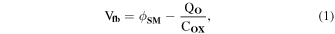
where ϕSM, QO, and COX show the work function difference between the gate electrode and the substrate, the fixed-charge density, and the gate oxide capacitance per area, respectively. Therefore, the Vfb shift, which was approximately 0.5 V, was caused by the work function difference between the manganese nitride compound and Al. Thus, as the work function of Al is 4.25 eV, which is close to the conduction band minimum of Si, the manganese nitride compound is estimated to be the mid-gap work function material. This work function difference affects the threshold voltage (VTH) of the MOSFETs. Thus, we should consider the effect of the work function difference in investigating the effect of the manganese nitride gate on the MOSFET characteristics.
To evaluate the effect of the manganese nitride gate without considering some factors, such as VTH, we investigated the electron mobility obtained via the split C–V method. 36) Figure 4(d) shows the electron mobility characteristics of the fabricated MOSFETs having a manganese nitride gate and an Al gate. MOSFETs with manganese nitride and Al gates were both fabricated through the same process, as shown in Fig. 3. We consider that the region higher than the difference between VG and VTH (VG−VTH) of approximately 0.8 V shows the region dominated by phonon scattering. In the phonon scattering region, the electron mobility of the MOSFET with the manganese nitride gate was 10% higher than that of the MOSFET with the Al gate. The FEM simulation results for the strain, which are illustrated in Fig. 3(d), show that an estimated 0.06% tensile strain was induced into the Si channel because of the manganese nitride gate. The relationship between strain and mobility enhancement rate, which was obtained in this study, is consistent with that in other reports. 37) Therefore, this increase in electron mobility can be attributed to the introduction of tensile strain by the negative thermal expansion gate. Consequently, the negative CTE material can introduce tensile strain into the channel of MOSFETs.
Finally, we investigated the applicability of the manganese nitride gates to the advanced MOSFETs. FinFET structures are used in advanced integrated circuits. Gate-all-around (GAA) structures with nanosheet channels are currently being considered for the further scaling of MOSFETs. Thus, we should also investigate the effect of the negative CTE materials on these structures in a bid to apply the negative CTE materials to the gate electrode of near-future MOSFETs. We investigated the effect of the manganese nitride gate on the SOI structure, FinFET structure, and GAA structure via FEM simulation. Figure 5 illustrates the structures used in the FEM simulation as well as the simulation results of the strain distribution in the MOSFETs. The current flow was along the x-direction in the figure. The results illustrate the normal strain in the current direction (εxx). The physical gate length and Si thickness of all structures were 15 nm and 5 nm, respectively, which were values used in the 7 nm technology node. 38,39) Figure 5(a) depicts the simulated structure and simulation result for the SOI structure. The results indicate the strain in the current direction. Here, we confirmed approximately 0.05% tensile stress in the Si channel, which is lower than that of the result presented in Fig. 3(d). The scaling of the MOSFETs was performed geometrically, whereas that of the physical thickness of the gate oxide was saturant recently. Thus, the gate oxide thickness indicated in Fig. 5 was larger than that of other materials compared with the gate oxide thickness indicated in Fig. 3. Therefore, the tensile strain induced by the manganese nitride was reduced.

Fig. 5. (Color online) Structures used in FEM simulation and the cross-section of the simulation results of the strain distribution in (a) SOI FET, (b) FinFET, and (c) nanosheet FET with the manganese nitride gate electrode.
Download figure:
Standard image High-resolution image
Figures 5(b) and 5(c) show the simulated structures and simulation results of the FinFET and GAA structures. We can observe a tensile strain larger than 0.1% in the Si channel. In these structures, the channel region was isolated from the substrate, and the overlap between the channel region and gate electrode increased. Thus, the negative manganese nitride gate can effectively introduce tensile strain into the Si channel.
To enhance electron mobility, we proposed to apply the negative CTE material as the gate electrode. The deposited manganese nitride thin film exhibited a negative thermal expansion. Hence, the fabricated MOSFET with the manganese nitride gate, having a negative CTE, indicated an enhancement in electron mobility. The use of negative thermal expansion materials as gate electrodes to introduce strain is a unique and unprecedented approach. Recently, the structure of MOSFETs has been changed to the FinFET structure and GAA structure from the planar structure, which was used in this study. The FEM simulation results indicated that the effect of the negative CTE gate structure increased in these structures. These results indicate that the negative CTE gate structure is promising for the scaling down of MOSFETs with FinFET or GAA structures.
Acknowledgments
This work was supported by KAKENHI JP20H02193, JP19K21953 and through the activities of VDEC, the University of Tokyo, in collaboration with Cadence Design Systems. The work was performed in the Micro/Nano-Machining Research and Education Center at Tohoku University.