
Abstract
In semiconductor processes, precise control of the wafer-in-process is a key parameter closely related to production yield, and the development of electrostatic chuck (ESC) continues towards higher chucking voltage with higher backside cooling gas. This study aims to determine the target temperature and uniformity of the wafer surface by varying the contact ratio of the ceramic-embossing facing the wafer-in-process. A computational fluid dynamics model with a thin wall boundary condition is considered to interpret the flow of the rarefied gas between the wafer and ceramic surface of the ESC. Through 3D simulations conducted with ANSYS Fluent, we observed temperature changes as the backside gas pressure varied from 1 to 9 Torr. The ESC with the highest contact ratio performed exceptionally well with an average temperature of 295 K and a coefficient of variation of 0.04%.
Export citation and abstract BibTeX RIS
1. Introduction
As semiconductor devices are continuously downsizing, vertical structure of the device process and integration is continuously developed to increase the capacity and functionality of the semiconductor chip. It more requires high aspect ratio (HAR) etch which guarantees not only critical dimensions with satisfying vertical etch profile, but also within wafer uniformity. Wafer-temperature control is a key parameter deeply related to process quality as well as chip production yield. 1–3) A small variation in a local temperature on the wafer-in-process causes a large deviation in the deposition and etching processes. 4–7) Thermal energy generated by atomic collision during the process was regarded the most suspicious reason, and it has been reduced by controlling temperature through an electrostatic chuck (ESC).
The ESC is an equipment part in the chamber which wafer-in-process lies on, and the wafer-temperature is controlled by coolant and helium gas flow inside the metallic base. Semiconductor etch technology, historically, has involved relatively small amount of RF power (<1 kW) to generate the plasma in the vacuum chamber, but the requirement of HAR pattern etch currently employs much higher RF power than ever (∼3 kW or even higher). Conventional holding and cooling the wafer-temperature from the wafer backside on ESC should also include the additional heating amount appears on the front side of the wafer from the increased ion bombardment of the plasma. 8–10) Wafer-temperature control by heat source has received considerable attention, and several coolant modeling has been patented. 11,12) Nevertheless, only a few scientific papers have been published on the design of backside gas flows that interact most closely with a wafer. The backside gas flows through the pattern of the ceramic, which is divided into contact and non-contact regimes.
Conduction by ceramic contact has a higher thermal conductivity than helium gas, and thus the average temperature of a chuck may be lowered, but there is a problem that causes non-uniformity due to contact resistance and surface roughness. Convection by helium gas is evenly distributed on all surfaces of the wafer to ensure uniform cooling. However, since it is governed by the backside gas, the average temperature depends on the gas pressure injected, and blowing can occur if sufficient chucking force is not guaranteed. 13,14) Furthermore, ESC possesses a chucking force in a state where the forces of Johnsen–Rahbek (J–R) and Coulomb coexist. The ratio of this force is determined by various factors such as the dielectric constant of ceramic materials, electrode positioning, shape, and other considerations.
Design optimization of the surface contact area and the backside gas flow can provide improved the heat transfer capability under high RF power condition to minimize the local temperature non-uniformity, which help the semiconductor etch process to be more successful, especially in HAR application. Therefore, we demonstrated the correlation of the contact area and backside gas pressure between ESC and wafer, and we propose a methodology for interpreting microfluidic flow using computational fluid dynamics (CFD) tools, which are commonly used in industry. We suggest an ESC model that can reach the target temperature and improve uniformity.
2. Theoretical modeling
2.1. Structural modeling
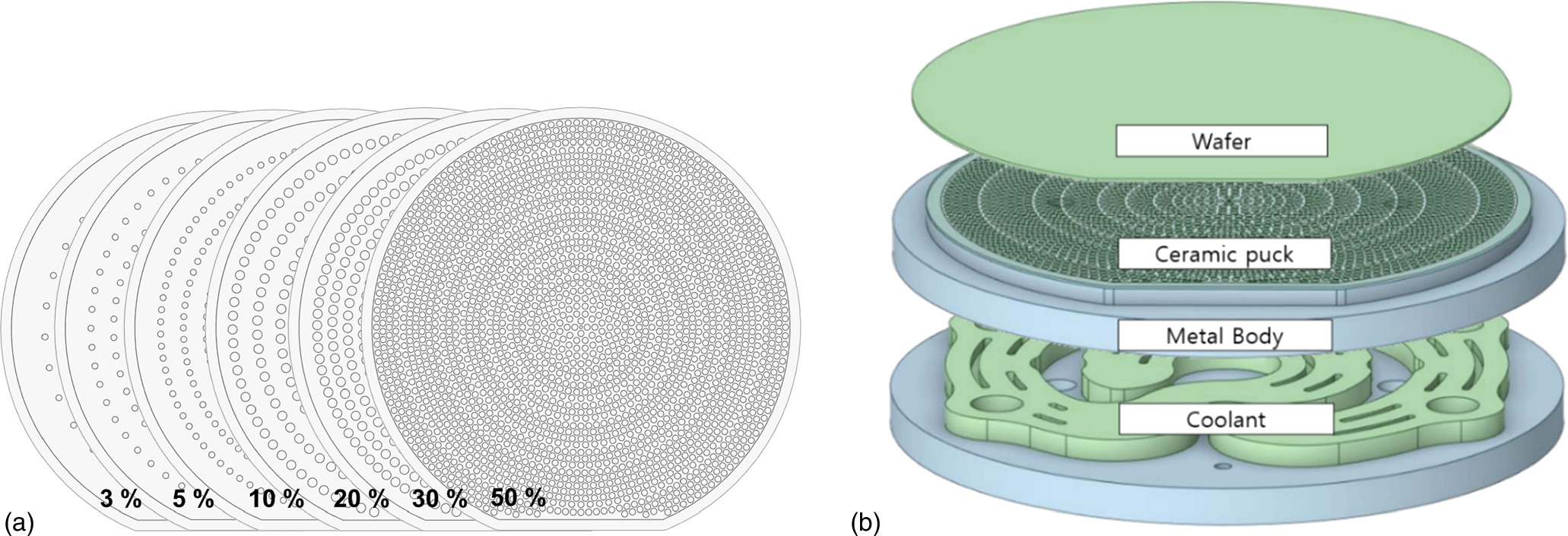
ESC consists of a metal body including a coolant path, a ceramic puck including an electrode, and an edge ring as shown in Fig. 1(a), and interfacial layer between the ceramic puck and the wafer is shown in Fig. 1(b). The micro-pattern between the ESC and the wafer is located, and a rarefied helium gas flows in the groove pattern on the ESC. The rest of the area other than groove region is defined with contact region. The contact region depends on the surface roughness of the material.

Fig. 1. A simplified schematic of ESC system; (a) inside chamber view of ESC with plasma and (b) a detailed interfacial schematic between the backside of the wafer and ceramic surface of ESC.
Download figure:
Standard image High-resolution imageThe targeting process equipment is inductively coupled plasma-reactive ion etching (ICP-RIE) located in the semiconductor process research center (SPDRC) at Myongji University, Korea. A 6 inch ESC is newly designed for the university research and development (R&D) with the goal of improving temperature uniformity. All parts of the ESC are designed in a 3D-solid structure, but the ceramic plate has a 2D-surface structure. The reason is that the tool used in the analysis (ANSYS Fluent 2021 R2) cannot directly calculate transition or free-molecular-region flows other than continuum flows. Therefore, we had to calculate and implement the 2D-surface structure to recognize it like a 3D-solid shape with an actual thickness value. This approach is depicted succinctly in Fig. 2. The method follows: (i) the 2D-surface creates a virtual wall thickness with a boundary condition in each contact area and groove area and (ii) the thermal conductivity considering the wall thickness was applied in each area to be calculated to enable thermal exchange between wafer and ceramic plate.

Fig. 2. Thin wall boundary condition method.
Download figure:
Standard image High-resolution image2.2. Electrical modeling
Considering a bipolar type of ESC employing Coulombic force, the desired chucking force for 6 inch silicon wafer was calculated with four capacities and electrostatic energy. 15–17) As presented in Fig. 1(b), δ is the air gap where helium is trapped due to the surface roughness of the ceramic plate, the thickness of bulk layer and helium gas in groove region was denoted by h and d. Furthermore, the 1D equivalent electrical circuit for a bipolar ESC using electrodes of opposite polarity is represented in Fig. 3. Each capacitance is represented by the formula below:


where C is capacitance,  is a permittivity of the vacuum,
  is a relative permittivity of the helium gas,
  is a relative permittivity of the bulk material, Ag is an area of the groove region and
  is an area of the contact region.
  and
and  are in series in the groove area, and
  and
and  are in series in the contact area. The total capacitance of the groove region and contact region can be calculated as below:


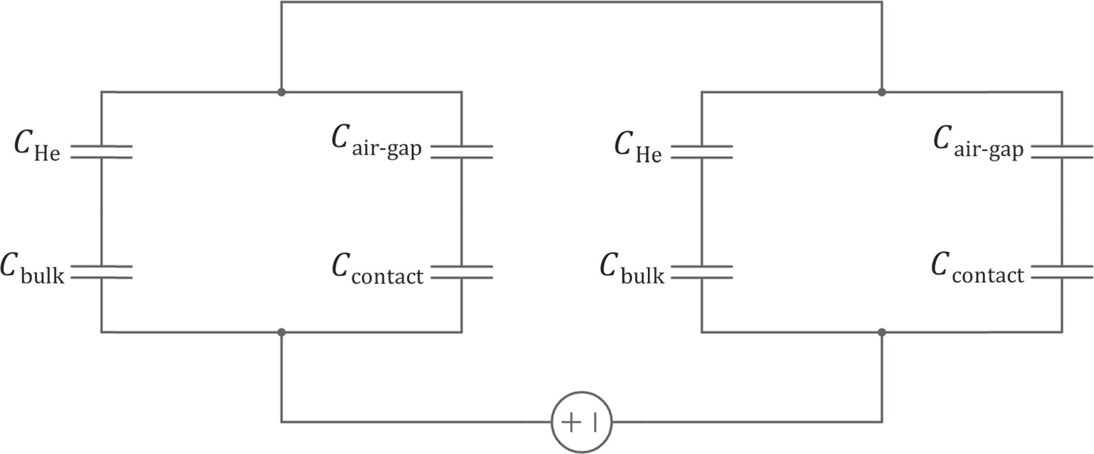
Fig. 3. 1D equivalent electric circuit of ESC.
Download figure:
Standard image High-resolution imageFinally, by calculating each Cg and Cc in parallel, the total capacitor is expressed as follows:
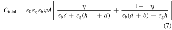


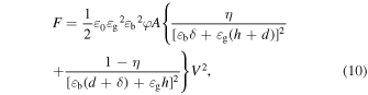
where η is the area ratio of contact region, φ is the area ratio of electrodes, and A is a total area of the bulk. The total capacitance can be used to calculate the electrostatic energy using Eq. (8) and the electrostatic force using Eq. (9). Therefore, it can be expressed as an electrostatic force that clamps the wafer in the contact/non-contact region of the ESC by Eq. (10). The magnitude of the electrostatic force represents the maximum pressure of backside gas that can be applied. It is straightforward that the electrostatic force is greatly affected by the diameter of the ESC (a 12 inch ESC has greater chucking force than 6 inches). In addition, in helium-dominated structures (e.g. where the contact area is less than 3%) and otherwise, this acts as a major factor in determining the temperature uniformity and average temperature of the wafer. Therefore, as the chucking force decreases, the pressure of the backside He gas that should also be decreases.
In this research, perhaps in 6 inch ESC, it is disadvantageous adopting helium-dominated structure. In fact, when the DC power was applied at 1000 V, the maximum pressure of the backside gas is limited to 9 Torr, and helium-dominated structure may not reach the target cooling temperature. However, if the diameter of the chuck is increased to accommodate higher DC power or the spacing of the electrodes is adjusted to enhance the chucking force, it may be possible to address the aforementioned issues. Additionally, caution must be taken regarding arcing issues caused by excessive use of DC power. The range of maximum backside gas pressure depending on the applied power is depicted in Fig. 4 for six different ESCs [as shown later in Fig. 6(a)] with varying contact ratios. The calculated maximum backside gas pressures are directly proportional to the chucking force, and the higher their values, the more advantages can be gained in a helium-dominated structure.
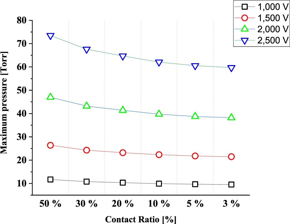
Fig. 4. Maximum backside gas pressure according to chucking voltage and contact ratios.
Download figure:
Standard image High-resolution image2.3. Thermal modeling
We determined whether the gas flow in the groove regions corresponds to the continuum, slip, transition, or free-molecule regimes using the Knudsen number. Helium gas flowing in patterns with a thickness of approximately 10 μm in the direction perpendicular to the groove, at a temperature of 300 K and a pressure range of 1 to 9 Torr, exhibits a minimum Knudsen number of 1.167. Knudsen number higher than 0.1 represents a transition flow or free-molecular flow scheme and flows in these high transitions or free-molecular regimes require direct solutions of Boltzmann's equations or models such as molecular dynamics or direct simulation Monte Carlo. 18) This was replaced by converting the heat transfer coefficient to thermal conductivity using the Boltzmann equation. 19–21)
This method uses the layer bulk model to calculate the heat transfer coefficient in the groove region and the contact region for CFD study. 22–25) Equation (11) for calculating the heat transfer coefficient in the groove and air gap, and an Eq. (12) for calculating the heat transfer coefficient for the spot contact according to surface roughness:
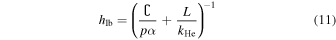

In Eq. (11), C is a gas-dependent constant, α is the thermal accommodation coefficient, and  is the thermal conductivity of helium gas. L is the thickness of the gas-layer between the wafer and the ceramic, δ + d for groove and δ for air-gap. In Eq. (12),
  is the combined average roughness defined by
  H is the surface microhardness,
  is the harmonic mean thermal conductivity of
  and P is the chucking pressure. The properties of Eqs. (11) and (12) have been summarized in Table I, and gas-dependent constant and thermal accommodation coefficient were derived by applying material properties and specific dimensions following the work of M. Klick et al.
26) The heat transfer coefficient for the groove region and for the contact region calculated here are as follows:
and P is the chucking pressure. The properties of Eqs. (11) and (12) have been summarized in Table I, and gas-dependent constant and thermal accommodation coefficient were derived by applying material properties and specific dimensions following the work of M. Klick et al.
26) The heat transfer coefficient for the groove region and for the contact region calculated here are as follows:


Table I. Properties for calculation.
| Component | Symbol | Value | Unit |
|---|---|---|---|
| Gas-dependent constant | C | 0.7 | Ks/m |
| Thermal accommodation coefficient |

| 0.6 | — |
| Surface microhardness | H | 10.2 | Gpa |
| Combined average roughness |

| 0.2 |

|
Through Eq. (15), the heat transfer coefficient is converted to thermal conductivity and applied to each region.

Utilizing Eq. (13) and (14), we computed the heat transfer coefficients in the backside gas region, employing them as simulation boundary conditions. These equations were also instrumental in calculating the thermal resistance for each component in the design. Notably, we observed that the thermal resistance in the backside gas region was higher compared to other components. Furthermore, the decrease in thermal resistance due to the increase in backside gas pressure can be observed in Fig. 5. 27) The advantages of increasing the backside gas pressure are clear.

Fig. 5. Thermal resistance values for backside gas pressure from wafer to coolant.
Download figure:
Standard image High-resolution image3. Experimental methods
The modeling used in the simulation is a 6 inch ESC with ceramic designs with 6 cases. This ceramic design was split as shown in Fig. 6(a) according to the contact ratio of 3%, 5%, 10%, 20%, 30%, and 50%. The contact ratio represents the proportion of the wafer's surface area that directly contacts the ceramic plate. As the contact ratio decreases, the influence of the backside gas pressure increases. The simulation model is briefly shown in Fig. 6(b). Heat flux was applied to the wafer surface to create an environment heated by the plasma, and the ceramic geometry was designed with a surface of zero thickness. The reason is that other parts are very large compared to the size of the ceramic feature, which can be disadvantageous in the process of generating a mesh. To solve this problem, we entered the wall thickness using the thin wall boundary condition with δ = 0.2 μm and d = 10 μm.

Fig. 6. 6 inch ESC designed for this research; (a) ceramic plate design with various contact ratios and (b) modeling of exploded view.
Download figure:
Standard image High-resolution imageThe heat flux utilized in the simulation was adopted from Y. D. Lim et al. 28,29) The heat flux applied to the Si substrate exposed in an Ar plasma environment, depending on the inductively coupled plasma (ICP) power, can be monitored through the thermal sensor system. Moreover, the heat flux allows observation of temperature discontinuities as it traverses various layers of components. Therefore, the analysis of components serving as heat sink sources is crucial, requiring meticulous mesh generation. When there is a significant scale difference in the structure, the number of mesh elements at the micro-scale can exponentially increase, leading to reduced accuracy due to unnecessary mesh refinement. Hence, we simplified the unnecessary structures in the model during the design process and refined the mesh elements near grooves and coolant paths. The simplified ESC mesh structure is illustrated in Fig. 7. The groove and coolant path areas were refined into three layers across intervals, while the remaining components were meshed as a single layer to facilitate a rational computation.
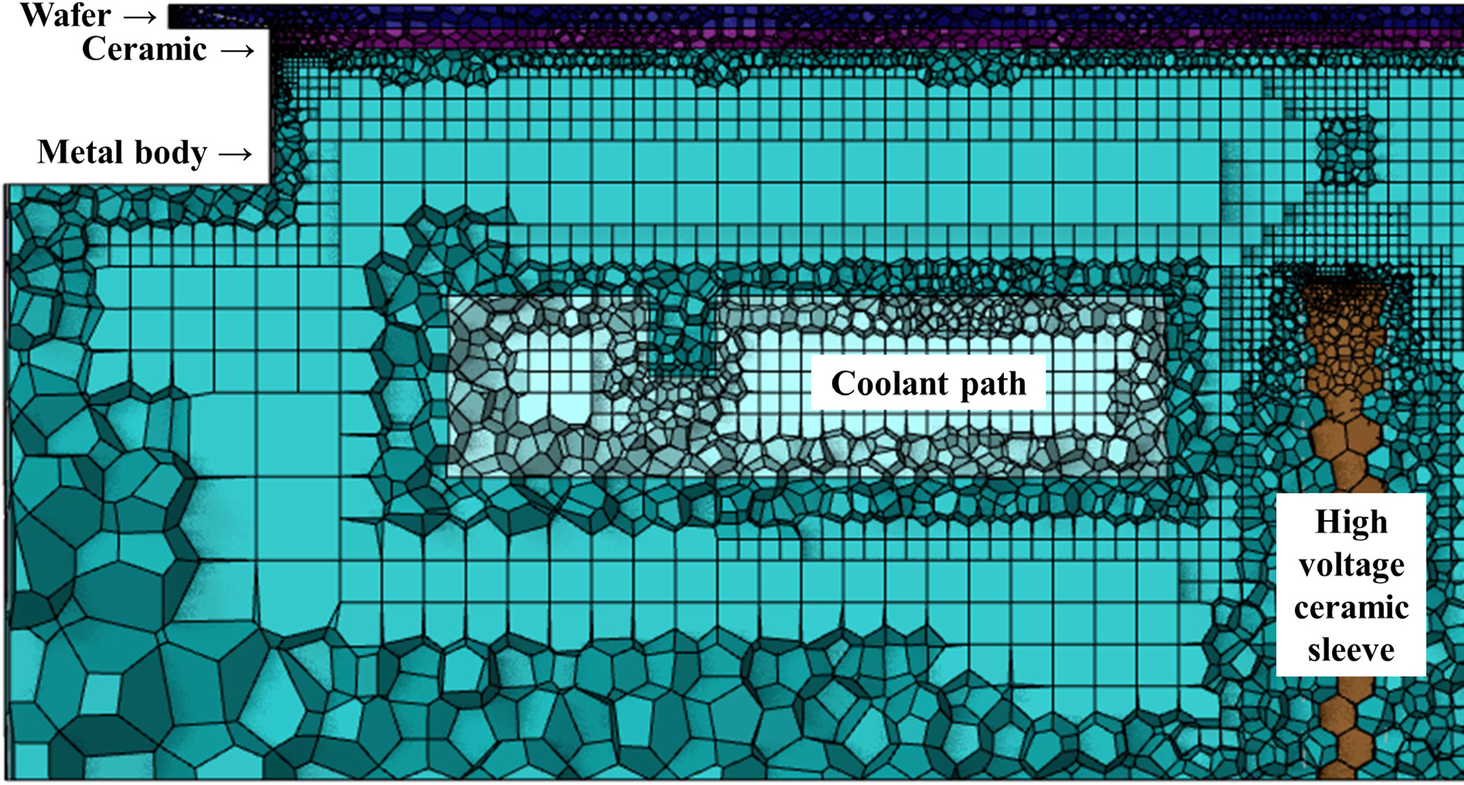
Fig. 7. Detailed section view of mesh generation for thermal fluid simulation.
Download figure:
Standard image High-resolution imageExperiments were conducted independently on six types of ESCs with varying contact ratios. Through correlation analysis between backside gas pressure and thermal resistance, we examined uniformity, average temperature, and temperature spectrum from the edge to the center of the entire surface. The backside gas, utilizing helium with high thermal conductivity and inert characteristics, was designed with a focus on improving temperature uniformity. 30) Detailed properties and boundary conditions are provided in Tables II and III.
Table II. Boundary conditions.
| Component | Value | Unit |
|---|---|---|
| Heat flux | 5500 | W/m2 |
| Backside gas pressure | 1 ∼ 9 | Torr |
| Coolant mass flow | 0.25 | kg/s |
| Chucking voltage | 1000 | V |
Table III. Material properties.
| Component | Material | Density [kg/m3] | Specific heat [J/kgK] | Thermal conductivity [W/mk] | Viscosity [g/ms] |
|---|---|---|---|---|---|
| Ceramic plate | Al2O3 | 3950 | 880 | 28 | — |
| Metal body | Al6061 | 2700 | 1020 | 167 | — |
| Wafer | Si | 2330 | 150 | 710 | — |
| Coolant | H2O | 998 | 4182 | 0.60 | 1.003 |
| Backside gas | He | 0.1785 | 5193 | 0.15 | 0.02 |
4. Results and discussion
The length from the electrode to the wafer is 250 μm, and an ESC that is clamped by a Coulomb force is investigated with CFD analysis. Total of 5000 points were designated on the wafer surface to obtain a temperature value. The average temperature of the wafer along the increase in backside gas pressure is illustrated in Fig. 8. When the contact ratio was 50%, the lowest average temperature was achieved with small amount of the backside pressure. In the range of 20%–50% contact ratio, the average temperature demonstrated an upward trend concurrent with an increase in backside gas pressure. Nevertheless, no discernible decrease or alteration was observed within the 3%–10% range. This observed trend underscores the necessity for designs that are dependent on backside gas pressure.
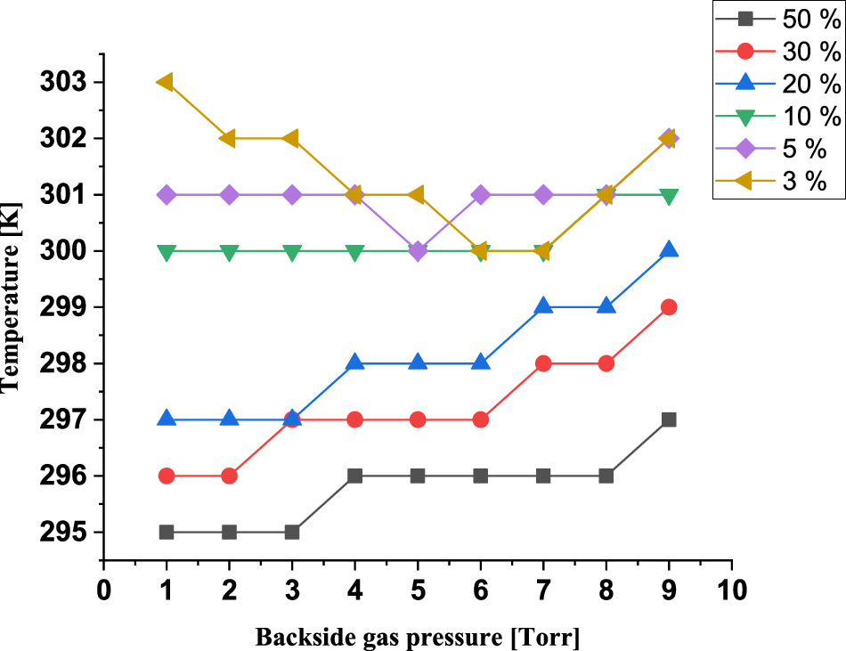
Fig. 8. Average temperature according to backside gas pressure.
Download figure:
Standard image High-resolution imageIt is imperative to ensure the provision of adequate backside gas pressure to achieve temperature uniformity, while concurrently ensuring that the surface is maintained at a sufficiently low temperature. In the case of the 6 inch ESC used in this experiment, a higher contact ratio is associated with the lowest temperature values, which may be misleadingly interpreted as an ideal design. As the diameter of the ESC increases, the required backside gas pressure also rises, and structures with higher contact ratios lose the advantages of uniformity and surface temperature provided by the backside gas. Therefore, in environments where a maximum backside gas pressure that does not cause blow-up is guaranteed, ESCs in the range of 3%–10% exhibit advantages over those with a contact ratio between 20% and 50%.
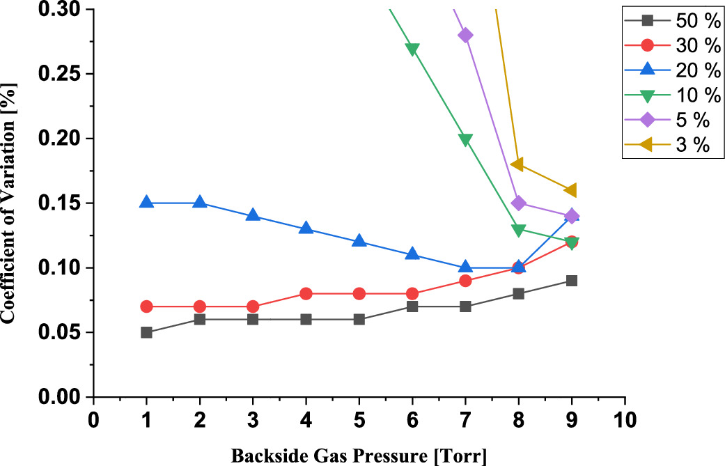
The uniformity of temperature distribution, expressed as the coefficient of variation, is illustrated in Fig. 9. The coefficient of variation serves as an indicator of which sample among different ESCs exhibits greater uniformity, with the level of uniformity expressed as a percentage. Further insights into the temperature uniformity of each ESC with increasing backside gas pressure are provided in Fig. 10. For models with a low contact ratio (3%–20%), increasing backside pressure resulted in improved uniformity. However, in models with a contact ratio of 30% and 50%, an increase in backside pressure led to a decrease in uniformity. Additionally, ESCs with a contact ratio of 3%–10% demonstrated a geometrically increasing improvement in uniformity as backside gas pressure increased.
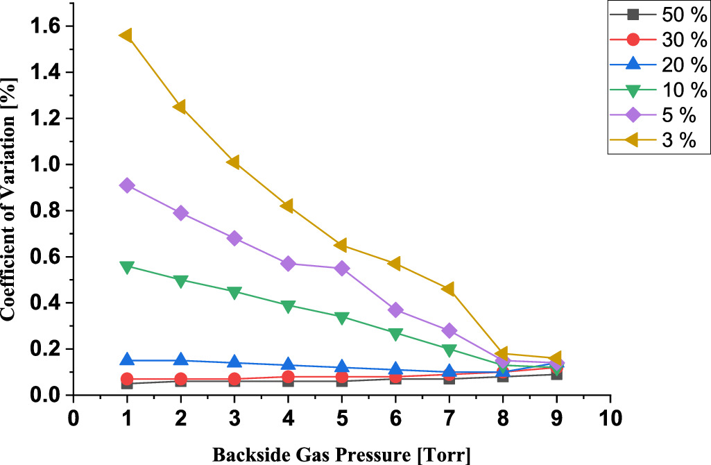
Fig. 9. Coefficient of variation according to backside gas pressure.
Download figure:
Standard image High-resolution image
Fig. 10. The coefficient of variation ranges from 0% to 0.3%.
Download figure:
Standard image High-resolution imageThe temperature distribution along the x-axis from the edge to the center of the ESC surface can be observed through Fig. 11. As the contact ratio decreases, the deviation between the center and edge becomes more pronounced, and it was observed to become more uniform with increasing backside gas pressure. This phenomenon is reminiscent of similar temperature distributions in ESC ceramics with edge ring patterns and high contact ratio dimple patterns. However, in dimple patterns with low contact ratios, significant variations were observed, likely due to dependence on helium. Nevertheless, these differences were mitigated with supplementary helium gas pressure. The temperature gap between the edge and the center can be observed in Fig. 12. At low backside gas pressure, a low contact ratio exhibits a larger gap difference, while at 9 Torr, a low contact ratio shows either a smaller gap difference or an equivalent gap difference.
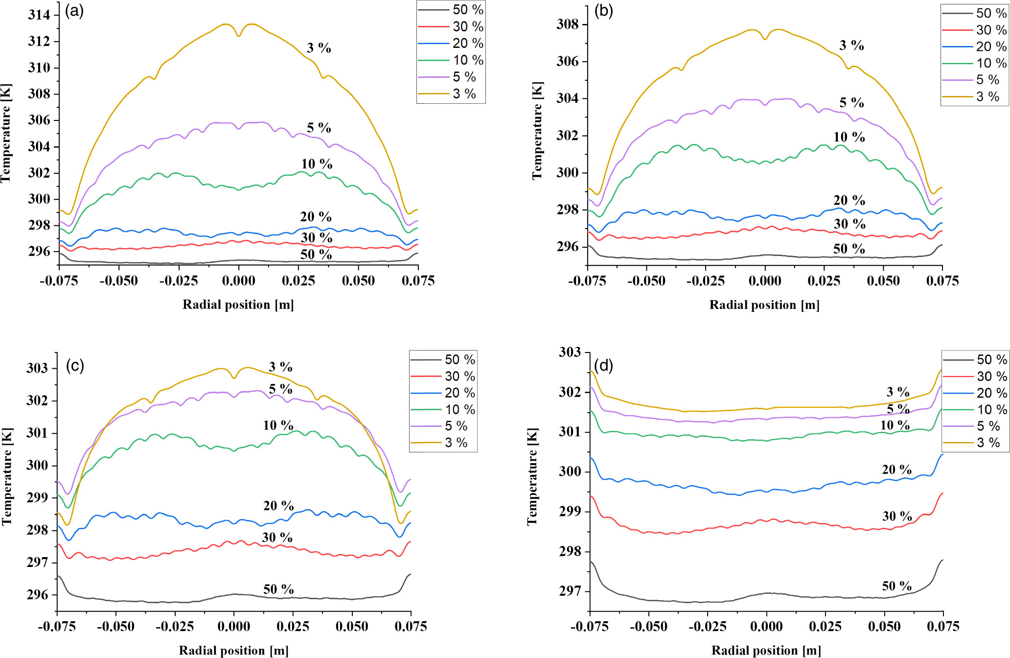
Fig. 11. The edge-to-center distribution along the x-axis under conditions of (a) 1 Torr, (b) 3 Torr, (c) 6 Torr and (d) 9 Torr.
Download figure:
Standard image High-resolution image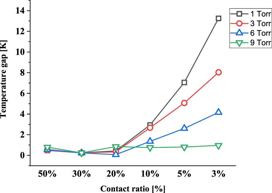
Fig. 12. The temperature gap from edge to center.
Download figure:
Standard image High-resolution image
5. Conclusions
In this study, we conducted a simulation of an ESC that generates chucking force through Coulomb interactions. In the case of the Coulomb force ESC, it has been confirmed that the chucking force increases with a higher contact ratio. It is important to consider the limit of the electrostatic force applied, which depends on the diameter of the ESC. A total of six ceramic patterns were utilized in the simulation.
Among them, the 6 inch ESC model with a 50% contact ratio, yielding an average temperature of 295 K and a relative coefficient of variation of 0.04%, was identified as the most suitable. However, this choice is contingent upon the limits of the permissible maximum backside gas pressure and is made to prevent blow-up phenomena. Through various experimental results, we confirmed that as the diameter of the ESC increases, the contact ratio should decrease. In structures with a low contact ratio, an increase in backside gas pressure leads to a geometrically improved temperature uniformity, coupled with a decrease in average temperature. Additionally, inadequate contact area may result in failure to reach the target temperature, while excessive contact area can induce non-uniformities. Therefore, having an appropriate contact ratio corresponding to the diameter of the ESC is crucial, and it is essential to maximize the utilization of the advantages offered by backside gas.
Acknowledgments
This research was supported by the Korea Evaluation Institute of Technology (KEIT) via Korea Semiconductor Research Consortium; GID 20022492) support program for the development of the future semiconductor device.