
Abstract
The availability of photoelectrical characterizations of heavily Al-doped p-SiC Schottky contacts was clarified. We conducted a systematic study of four samples with different Al doping concentrations from 1 × 10¹⁸ to 5 × 1019 cm−3. Although the current–voltage (I–V) characteristics had lost rectification, reasonable Schottky barrier height (qϕB) values were obtained up to 1 × 1019 cm−3 by capacitance voltage, photo response, and scanning internal photoemission microscopy (SIPM) measurements. In the two-dimensional characterization by SIPM, large photocurrent spots corresponding with low qϕB were observed in an average density of 103 to 104 cm−2. However, except for these spots, a high uniformity of about 2 meV standard deviation was obtained for qϕB over the entire observed electrodes. These results indicate that SIPM is able to characterize the inhomogeneity of heavily doped p-SiC contacts with very leaky I–V characteristics.
Export citation and abstract BibTeX RIS
1. Introduction
SiC has attracted wide attention as a material for the next generation of high-power devices because of its advantages of a high breakdown voltage, low on-resistance, the availability of both p- and n-types, 1–4) and the availability of a large size single crystal wafer (up to 8 inches). 5,6) To date, high-power devices, such as metal-insulator-semiconductor (MOS) FET, 7) SiC bipolar junction transistors, 8) PiN diodes, 9) thyristors, 10) and insulated gate bipolar transistors 11,12) have been demonstrated to operate above 10 kV. In recent years, not only high-power performance but also downsizing and integration have been studied intensively. As SiC MOSFET structures have become more complex, the formation of better ohmic contacts is required to p-well and p-body regions in a small electrode area. 13) However, fewer studies have been done on ohmic contacts for p-type SiC than n-type SiC. It has been reported that contact resistances were in the range of 10−6 Ω cm2 for Ni/n-4H-SiC annealed at 1000 °C 14,15) and 10−4−10−5 Ω cm2 for Al/Ti and Ni/Al/p-4H-SiC annealed at 900 °C–1000 °C. 16,17) In ohmic contact formation, impurity doping density, annealing conditions, electrode metal selection, and surface treatment before metal deposition are major issues. In this paper, we focus on the effects of doping density without annealing in order to reveal basic electrical characteristics of metal/heavily doped p-SiC contacts in an intermediate state between Schottky and ohmic contacts. From the aspect of measurement methods, we used photoelectrical methods, photoresponse (PR), and scanning internal photoemission microscopy (SIPM), in addition to conventional current–voltage (I–V) and capacitance–voltage (C–V) methods. Especially by using SIPM, which we originally developed for non-destructive two-dimensional characterization of metal/semiconductor (M/S) interfaces covered with a thick metal, 18,19) there was an advantage in investigating inhomogeneity over the electrode in photocurrent and Schottky barrier height (qϕB) images. Actually, we have demonstrated SIPM for lightly doped SiC Schottky contacts (n-4H-SiC (n = 1016 cm−3) and p-6H-SiC (p < 1015 cm−3)) with excellent I–V characteristics to visualize typical crystal defects, such as stacking faults, downfalls, and pits in the vicinity of the SiC surfaces. 20)
In this study, although the measurement equipment used was the same as in our previous studies, a systematic study on the doping density was conducted for heavily doped Au/Ni/p+-SiC Schottky contacts with very leaky I–V characteristics and with four different Al acceptor doping concentrations from 1 × 10¹⁸ to 5 × 1019 cm−3. In our preliminary report, 21) SIPM measurements using a red laser (λ = 659 nm) were conducted for the Au/Ni/heavily Al-doped p-SiC Schottky contacts. In this paper, we report additional experiment results: (i) SIPM measurements by using a green (λ = 525 nm) laser; and (ii) qϕB images of the contacts, which were obtained from the SIPM measurements. Then, we discuss the electrical inhomogeneities in one electrode by using qϕB histograms, which are important for estimating the current distribution across the M/S interface.
2. Experimental methods
Figure 1 shows (a) the device structure of Au/Ni/p+-SiC Schottky contacts with measurement circuits and (b) the device fabrication process. Layers of p+-SiC 10 μm thick with four different Al concentrations (1 × 1018 cm−3 for Sample I, 3 × 1018 cm−3 for Sample II, 1 × 1019 cm−3 for Sample III, and 5 × 1019 cm−3 for Sample IV) were grown on N-doped n-4H-SiC substrates. The Al doping concentrations were estimated from the growth conditions. The uniformity of doping concentration, evaluated by non-contact C–V measurements, was about 5% across the entire 3" to 4" wafers. The wafers were cut to yield specimens of approximately 10 mm square from the central regions of the wafers. After surface treatments with H2SO4/H2O2, HF(aq), and HCl(aq), circular Schottky contacts (200 μm in diameter) consisting of 50 nm thick Au and 50 nm thick Ni layers were deposited on the p+-SiC surfaces by using electron beam evaporation. Note that the samples were not annealed. Then, InGa ohmic electrodes were deposited on the p+-SiC surfaces on the edge of each 10 mm square sample.

Fig. 1. (a) Sample structure with measurement circuits and (b) device fabrication process of the Au/Ni/heavily Al-doped p-SiC Schottky contacts.
Download figure:
Standard image High-resolution imageFor all the electrical measurements, the InGa ohmic contact was commonly used as the earth. The electrical circuits between the Au/Ni Schottky and InGa ohmic contacts in the individual measurements are shown in Fig. 1(a). First, we measured the I–V characteristics by using an HP4142B semiconductor parameter analyzer. The detection limit of a current in this system is less than 10−13 A.
Next, we conducted C–V measurements swept from 0 to 10 V at a frequency of 1 MHz by using an HP 4284 A LCR meter. The C–V relationship for a Schottky contact is


where ε is the permittivity (εSiC = 9.7 ε0), Na is the acceptor concentration, and Nv is the effective density of state (Nv = 1.3 × 1019 cm−3) based on Nv = 2(2πm* kT/h2)3/2. 22) Then, we calculated the qϕB and the Na of the samples from the 1/C2–V characteristics.
Prior to the SIPM measurements, we conducted conventional PR measurements. Since we used the same measurement equipment as in our previous reports, details of the PR and SIPM measurements are described in Refs. 19, 20. When a monochromatic light with a photon energy (hν) greater than qϕB is irradiated on the Ni/p+-SiC interface, carriers in the metal can surmount the Schottky barrier and a photocurrent can be generated. This is known as the internal photoemission effect. The qϕB can be determined from the measured photocurrent using Fowler's equation: 23,24)

where Y is the photo yield, which is a photocurrent per incident photon count, and A is a constant. If we consider the physical origin of the Y signal, A is an efficiency to excite carriers and generate photocurrent by photon irradiation, and qϕB is an energy barrier that carriers surmount. This paper reports qϕB images in addition to Y images. This is an advantage in understanding the physical model compared to our preliminary report. 21) In the PR measurement, the entire contact was irradiated with monochromatic light with a wavelength from 350 to 1100 nm, and the generated photocurrent was detected between the Au/Ni and InGa contacts without an applied external voltage, as shown in Fig. 1(a).
For the SIPM measurement, red (λ = 659 nm) and green (λ = 525 nm) laser beams were focused and scanned over the contact to obtain a two-dimensional image of Y. In addition, using the Y values irradiated by each laser beam at the same location, we also obtained the qϕB images. The estimated beam spot diameter at the interface was less than 2 μm.
3. Results and discussion
Figure 2 shows the (a) forward and (b) reverse I–V characteristics of ten Au/Ni/p+-SiC Schottky contacts in every sample. Very leaky I–V characteristics were obtained for all the samples. The average current values of the ten electrodes at +2 and −2 V were 9 × 10⁻⁶ and 2 × 10⁻⁶ A for Sample I, 2 × 10⁻⁵ and 1.5 × 10⁻⁵ A for Sample II, 8 × 10⁻⁴ and 1.5 × 10⁻⁴ A for Sample III, and 1.5 × 10⁻² and 1.5 × 10⁻² A for Sample IV, respectively. Similar to conventional current transport mechanisms in a high doping concentration, we confirmed that the leakage current increased with an increase in the doping concentration. Therefore, we could not obtain the qϕB values from these I–V characteristics. We also observed large diode-to-diode variations in the reverse biased current characteristics of Sample I. Supposing that there are some low qϕB regions in the electrode (low qϕB spots shown in the SIPM results described below), which induce a leakage current, the smaller reverse currents of Sample I are sensitive to such a leakage current compared to other samples with larger background currents.
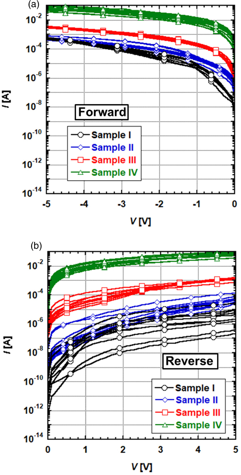
Fig. 2. (a) The forward and (b) reverse I–V characteristics of the Au/Ni/heavily Al-doped p-SiC Schottky contacts.
Download figure:
Standard image High-resolution imageFigure 3 shows the 1/C2–V characteristics of ten Au/Ni/p+-SiC Schottky contacts in every sample. Good linearity is seen up to 7 V for Sample I, 10 V for Sample II, and 3 V for Sample III. No linear region was observed over the entire voltage range in Sample IV, probably due to the very leaky I–V characteristics. From the linear regions, we obtained the qϕB values and Na of 1.69 eV and 1.0 × 1018 cm−3 for Sample I, 1.88 eV and 1.9 × 1018 cm−3 for Sample II, and 1.68 eV and 7.7 × 1018 cm−3 for Sample III.

Fig. 3. 1/C2–V characteristics of the Au/Ni/heavily Al-doped p-SiC Schottky contacts.
Download figure:
Standard image High-resolution imageThe PR spectra of the ten Au/Ni/p+-SiC Schottky contacts for each sample are shown in Fig. 4. For Samples I, II, and III, large peaks and tailings on the lower-energy side of the peak were observed, which were similar to those of the Au/Ni/p-6H-SiC Schottky contacts in our previous report. 25) No clear signal was obtained from Sample IV, nor from the C–V. In the PR spectra of Samples I, II, and III, the Y1/2 values linearly increased from 1.5 to 2.3 eV. This was caused by the internal photoemission. We applied Eq. (3) to the linear regions and obtained the qϕB values of 1.52, 1.51, and 1.44 eV for Samples I, II, and III, respectively. In the hν range from 2.5 to 2.7, the Y signal decreased, and finally, at around 2.7 eV, the Y signal was almost at the noise level. It is considered that the incident light from the semiconductor side did not reach the interface because of the absorption associated with the doped N donors in the 4H-SiC substrate. 26) Then, in the higher energy region, peaks at about 3.3 eV appeared due to the fundamental absorption in the depletion layer. Lights with a higher energy than 3.3 eV were completely absorbed in the SiC substrate and did not reach the interface, resulting in no Y signal. From the PR spectra, we speculated that the qϕB values could be obtained by using red and green lasers in the SIPM measurements.

Fig. 4. PR spectra of the Au/Ni/heavily Al-doped p-SiC Schottky contacts.
Download figure:
Standard image High-resolution imageWe conducted SIPM measurements to evaluate the two-dimensional characterization of the Y distribution over the electrode. Figure 5 shows the SIPM Y images using the (a) red and (b) green lasers, and the optical microscope images of the electrode surface in (c) bright field and (d) dark field for Samples I, II, and III. We also observed the SiC surfaces using (e) a Nomarski microscope after etching the electrodes. As shown in Figs. 5(a) and 5(b), clear patterns of the 200 μm diameter electrodes were observed in the Y images for Samples I, II, and III. We also found bright spots that were approximately 10 μm in size in the area where Y was about 20% larger than that of the surrounding area for Samples I, II, and III, as indicated by the dashed circles in the Y images. The typical number of spots in one electrode was from one to seven; the corresponding density was from 103 to 104 cm−2, regardless of the doping concentration. In the bright-/dark-field images of the electrode surface and the Nomarski image of the SiC surface after etching the electrode, no contrast was found corresponding to the bright spots. On the other hand, Y was uniform over the electrode except for the bright spots.
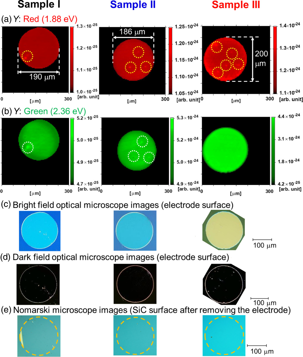
Fig. 5. SIPM Y images using (a) red and (b) green lasers, (c) bright-field and (d) dark-field optical microscope images of the electrode surface, and (e) Nomarski microscope images of the SiC surface after etching the electrode for Samples I, II, and III.
Download figure:
Standard image High-resolution imageUsing the Y values of red and green lasers, we obtained qϕB images, shown in Fig. 6(a). In all the images, a few low qϕB spots corresponding to the bright spots in the Y images were observed. The qϕB values decreased by about 50 meV corresponding to the bright spots.

Fig. 6. (a) SIPM qϕB images of the same electrodes shown in Fig. 5 and (b) histograms of all the qϕB pixels in the images with calculated fitting curves based on the normal distribution function for Samples I, II, and III.
Download figure:
Standard image High-resolution image
In order to investigate the variation in one electrode in more detail, each measurement point in the qϕB image was treated as a pixel, and histograms of all the qϕB pixels of the contacts were prepared, as shown in Fig. 6(b). The distributions can be divided into a sharp peak for the uniform regions and a tail in the lower-energy side due to the low qϕB spots. When peaks excluding low-barrier spots were fitted with a normal distribution function, the average qϕB values were 1.46 eV for Sample I, 1.48 eV for Sample II, and 1.44 eV for Sample III. The standard deviations were around 2 meV.
Table I shows a summary of the measured and reported Na, qϕB values, and the standard deviations of Ni Schottky contacts on p-type or n-type SiC. First of all, regarding the availability of characterization for the heavily doped p-SiC contacts, in this study, the I–V characteristics were too leaky to determine the qϕB value for all the samples, whereas the C–V, PR, and SIPM measurements could determine qϕB up to the doping concentrations of 1 × 1019 cm−3 for Samples I, II, and III. For highly doped p-SiC contacts, these measurements were more appropriate than I–V.
Table I. Summary of the obtained and reported carrier concentration, qϕB, and σ values.
| Ni/p+-SiC Sample I | Ni/p+-SiC Sample II | Ni/p+-SiC Sample III | Ni/p+-SiC Sample IV | Ni/p-SiC 25) | Ni/p-SiC 27) | Ni/p-SiC 28) | Ni/n-SiC | |
|---|---|---|---|---|---|---|---|---|
| Doping conc. (cm−3) | 1.0 × 10¹⁸ | 3.0 × 10¹⁸ | 1.0 × 10¹⁹ | 5.0 × 10¹⁹ | 9.0 × 10¹⁶ | 5.0 × 10¹⁵ | 5.0 × 10¹⁵ | 1.2 × 10¹⁶ |
| Na (cm−3) | 1.0 × 10¹⁸ | 1.9 × 10¹⁸ | 7.7 × 10¹⁸ | — | 8.9 × 10¹⁶ | — | 4.9 × 10¹⁵ | — |
| qϕB (I–V) (eV) | — | — | — | — | 1.31 | 1.31 | 1.56 | 1.47 20) |
| qϕB (C–V) (eV) | 1.69 | 1.88 | 1.68 | — | 1.84 | 1.56 | — | 1.57 20) |
| qϕB (PR) (eV) | 1.52 | 1.51 | 1.44 | — | — | — | — | 1.70 20) |
| ave. qϕB (SIPM) (eV) | 1.46 | 1.48 | 1.44 | — | — | — | — | 1.74 29) |
| σ (meV) | 1.93 | 1.75 | 2.88 | — | — | — | — | 0.84 29) |
Secondly, we compared our qϕB values with reported values. It has been reported that the qϕB values of Ni/low-Al-doped p-4H-SiC Schottky contacts (Na = 5 × 10¹⁵–9 × 1016 cm−3) ranged from 1.31 to1.84 eV according to the I–V and C–V measurements, as shown in Table I. 25,27,28) We calculated the qϕB decrease by image force lowering to be 011, 0.13, and 0.18 eV for Samples I, II, and III, respectively. 30) Upon determination of the qϕB value, in the PR measurement, because carriers in the metal were excited by the incident light and surmounted the energy barrier (qϕB), the measured qϕB value decreased by image force lowering from the original qϕB value. On the other hand, in the C–V measurement, because the potential curve at the end of the depletion layer was extrapolated to the M/S interface, the qϕB value was determined without image force lowering. Therefore, taking into account the lowering, the qϕB values measured by the PR became close to those of the C–V for Samples I and III within a range of 1.62–1.69 eV. Since these values were in the range of the reported qϕB values of the low-doped p-4H-SiC Schottky contacts above, we can conclude that reasonable qϕB values were obtained in this study. However, for Sample II, the qϕB value of 1.64 eV obtained from the PR results was reasonable, but the qϕB value of 1.88 eV obtained from the C–V was exceptionally high. The reason is not clear at this moment, but a possible explanation is that donor-type defects or impurities may be introduced in the vicinity of the SiC surface, which compensate for the Al acceptors and increase the qϕB value measured by C–V measurement. Since we conducted Schottky metal deposition by using electron beam evaporation at the same time for all the samples, there may be a problem at the end of the process of the SiC epitaxial growth or the surface treatment just before loading the sample into the evaporation chamber.
Focusing on the uniformity over the electrode in the SIPM results, we found 10 μm large bright spots (20% larger Y and 50 meV lower qϕB) with a density of from 103 to 104 cm−2, with no corresponding pattern in the microscopy observations of Samples I, II, and III and no Al-doping-concentration dependence. There was information from the substrate vender that the etch pit density (EPD) of the epitaxial SiC layers was about 104 cm−2. This value is consistent with our spot density. The EPD represents a dislocation density in general, but a single dislocation itself is not visible by SIPM because the size is much smaller than the spatial resolution of SIPM (less than 2 μm). One possible explanation is segregation of doped Al acceptors along the dislocations. The localized segregation of highly doped regions can lower the qϕB values. As these spots may induce the leaky I–V characteristics, additional statistical measurements to correlate between the number of spots and the leakage currents for mediumly doped contacts are of interest. In any case, microscopic analysis for the dopants and defect structures around the bright spots is required in further studies.
Finally, we discuss the qϕB uniformity in one electrode, excluding the bright spots. In a general Schottky contact, forward-current distribution over the electrode can be estimated by the σ value. The obtained σ values shown in Fig. 6(a) were as small as 1.93, 1.75, and 2.88 meV for Samples I, II, and III, respectively. Our comparative results of the qϕB uniformity across major wide bandgap semiconductors are also shown in Table I. It was confirmed that the σ values of the p+-SiC contacts were comparable to the n-SiC, n-GaN, and n-α-Ga2 O3 Schottky contacts. 29) These small σ values provide useful information for the downsizing and reproducibility of power devices.
These results indicate that PR and SIPM measurements are available to characterize heavily doped p-SiC contacts. In this study, the samples were not annealed, but in a future study, annealing studies of these samples would be valuable to understand current transport mechanisms in the initial stage of ohmic formation, especially two-dimensional characterization by SIPM.
4. Conclusion
We conducted a systematic study of doping concentration in heavily Al-doped p-SiC Schottky contacts with different Al doping concentrations from 1 × 10¹⁸ to 5 × 1019 cm−3 in order to clarify the availability of the photoelectrical characterization. Although the I–V characteristics lost rectification, reasonable qϕB values were obtained by the C–V, PR, and SIPM measurements up to 1 × 1019 cm−3, corresponding with the reported values of the Ni/low-Al-doped p-SiC Schottky contacts. In the SIPM results, bright spots that were approximately 10 μm in size with a density of 103 to 104 cm−2 were found regardless of the doping concentration, where Y was about 20% larger than that of the surrounding area. In the spots, the qϕB values decreased by about 50 meV, but no corresponding pattern in the microscopic images was found. However, a high qϕB uniformity with σ of around 2 meV was obtained in one electrode except for the spots. This uniformity was comparable to those of typical low-doped wide bandgap semiconductor Schottky contacts such as n-SiC, n-GaN, and n-α-Ga2O3. These results indicate that SIPM is able to characterize the inhomogeneity of heavily doped p-SiC contacts with very leaky I–V characteristics.
Acknowledgments
A part of this work was supported by a Grant-in-Aid for Scientific Research (C) 21K04135 of the Ministry of Education, Culture, Sports, Science, and Technology.
Supplementary data (0.5 MB PDF)