
Abstract
Wafer bonding is a key process in heterogeneous photonic integration and benzocyclobutene (BCB) is widely used for adhesive wafer-to-wafer bonding when it comes to handling complex topography on both wafers. However, until now a major drawback of bonding with BCB was the high thermal impedance of lasers due to the low thermal conductivity of BCB. We demonstrate, that by optimizing the membrane device topography and introducing the BCB reflow step into the process flow it is possible to achieve full planarization of 1 μm topography at the wafer scale while ensuring only 135 nm of BCB between the laser p-contact and the substrate. We show experimentally, that the thermal impedance of 500 μm long distributed feedback (DFB) laser was reduced from 585 to 271 K W−1 when bonded to Si substrate, and to 174 K W−1 when bonded to SiC substrate using the new method.
Export citation and abstract BibTeX RIS

Content from this work may be used under the terms of the Creative Commons Attribution 4.0 license. Any further distribution of this work must maintain attribution to the author(s) and the title of the work, journal citation and DOI.
1. Introduction
According to Moore's Law, the number of components in a microelectronic chip grows exponentially from year to year, while the size of a single component shrinks. 1) The same law can be applied to photonic integrated circuits (PICs). 2) InP-based photonics experienced rapid growth until the last decade; however, it is now approaching a limit of component density on a chip. 3) This limitation is mainly due to weak optical mode confinement in InP waveguides, forcing InP photonics to use relatively wide waveguides of 1.5–2 μm. 4) Heterogeneous integration of InP with Si or SiNx photonics helps overcome the density bottleneck. 5) In the context of heterogeneous integration, InP membranes bonded to Si 4) or SiC 6) are an emerging trend that can potentially demonstrate even higher integration density thanks to high index contrast in the membrane waveguides, ensuring high optical confinement. Another bottleneck PICs face is the speed limitation of optoelectronic transceivers imposed by the packaging of the photonic die. 7) Wafer-to-wafer bonding of electronics and photonics allows an unprecedented reduction in the length of radio frequency interconnects and thus enables compact and high-speed optoelectronic transceivers. 8) InP membrane on Si (IMOS) is a promising candidate for photonic–electronic wafer scale co-integration. 9) This platform unites in a single photonic layer semiconductor optical amplifiers (SOAs) and highly confined passive InP waveguides with cross-sections comparable with Si-on-insulator (SOI) waveguides. 4) The IMOS process flow allows processing on both sides of the membrane (the top side is processed before bonding on the native InP substrate and the bottom side is processed after bonding to Si and removing the native substrate) which gives a new degree of freedom to designers of ultra-fast optoelectronics. 10)
One of the biggest challenges for heterogeneous integration, compared to generic InP or GaAs photonics, is the thermal management of lasers. The heat generated inside the laser under continuous current injection can severely affect the laser performance if not extracted. 11) For membrane lasers, typically, the bonding layer reduces the heat flow from the laser core to the substrate, leading to high thermal impedances on the order of a few 100 to a few 1000 K W−1. Several ways to overcome this drawback were demonstrated. Firstly, the p-contact or both n and p-contact of a laser can be connected to the substrate by a metal shunt, as in Ref. 12 or in Ref. 13. With a shunt, continuous wave (CW) operation up to 110 °C was demonstrated for hybrid InP lasers on SOI. However, the necessity to fabricate a shunt requires at least one extra lithography step to open the bonding layer, making the processing more complicated. In addition, it increases the overall footprint of the device, compromising the integration density.
Another promising direction is the reduction of the thickness and thermal resistivity of the bonding layer and the substrate. This method has demonstrated advantages for hybrid integration by the micro-transfer printing method since it is possible to achieve a high-quality bond even with a very thin adhesive layer (tens of nm) for a coupon of a small area (compared to the size of the substrate). 14) However, die-by-die bonding has limitations related to the minimum coupon size and adiabatic mode conversion length, which makes it less promising for the fabrication of ultra-compact devices.
An outstanding reduction of on-chip heating can be achieved by combining a thin (less than 100 nm) adhesion layer and a high thermal conductivity substrate, such as SiC, as demonstrated in Refs. 15 and 16. For wafer-scale integration, recently RT direct bonding on surface-activated SiO2 helped to reduce the thermal impedance, 17) also on a 2 inch wafer scale with SiO2 thickness of only 10 nm. 18) However, the process of direct surface-activated bonding on SiO2 puts high requirements on surface cleanness, low roughness, and a high level of planarization; otherwise, defects are inevitable on a wafer scale. That is why direct bonding is mostly used for active devices with lateral current injection, such as in Ref. 19.
In the case of IMOS, a diverse topography is created on the wafer (with step heights of up to 1.5 μm) to exploit the full potential of photonics functionality. IMOS lasers use a vertical current injection scheme, enabling lower diode resistance and higher power output relative to lateral injection schemes. However, it also requires a laser mesa with trenches around it. The laser topography and the necessity of integration with electronics make direct bonding on SiO2 a very impractical solution. In contrast, bonding with adhesive polymers, such as benzocyclobutene (BCB), offers much more relaxed tolerances on surface topography and the size of particles present in the area during the bonding process. The thickness of the bonding layer can be easily fine-tuned to satisfy the needs of a particular design by using different dilution ratios. BCB can be spun in a liquid phase on a wafer with arbitrary topography, and then the planarization is achieved during the curing process. 20) This makes BCB a promising candidate for the bonding of high-topography and high-density active photonic membranes for co-integration with electronics. BCB has a low thermal conductivity constant of 0.293 W mK−1, which is advantageous to reduce thermal crosstalk between devices for high-density integration, but it also prevents the heat inside the laser from escaping through the substrate. Thus, the reduction of the BCB layer thickness is usually advantageous to reduce the thermal impedance of bonded InP lasers. 21,22) Bonding of flat 2 inch InP wafers on planarized SOI was reported previously with BCB thickness of 40 nm. 23) However, it was challenging to achieve a defect-free uniform bonding on a 3 inch wafer scale with BCB thickness below 500 nm for non-planar wafers with complex topography, and no such experiments were previously reported.
In this paper, we propose a novel bonding process to reduce the thermal impedance of InP membrane lasers, fabricated as a part of complex topography photonic circuits, using ultra-thin BCB as an adhesive layer. We achieve defect-free bonding on a 3 inch wafer scale, while the thickness of the BCB between the laser contact metal and the substrate is only 250 nm (wafer bonded to Si). The same technology allows for as thin as 135 nm BCB, which we achieved with a membrane bonded to a SiC wafer. At the same time, the devices on the wafer have step heights of up to 1 μm.
2. Methods
In a semiconductor laser, two major heat sources are typically found: (1) the active core, where the heat is caused by non-radiative recombination of carriers (such as Auger recombination); (2) the p-doped region, which has higher resistance than the n-doped region due to lower mobility of holes. 24) This is why it is essential to ensure the p-contact is as close as possible to the heat sink. In IMOS technology, the epitaxial layer stack for the laser is grown in the order from n-contacts to p-contacts, which is important to reduce p-dopant diffusion to the core. Thus, initially, the p-contact is the top layer, and after bonding, since the original InP wafer is flipped, the p-contact becomes the closest to the substrate part of the laser [see Fig. 1(a)]. This is beneficial for the fabrication of a heat sink.
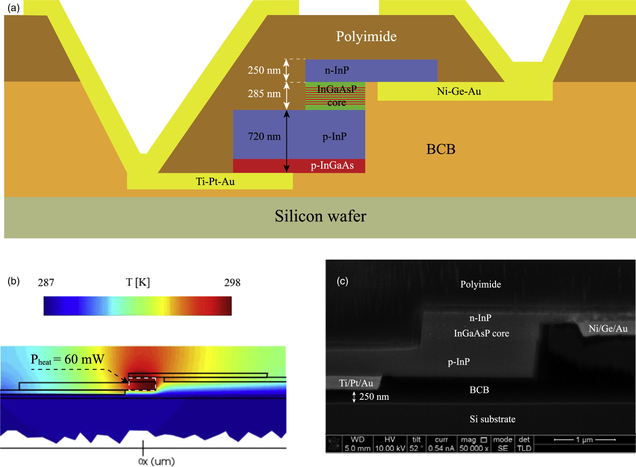
Fig. 1. (a) Schematic cross-section of the IMOS laser. The passivation layer of SiO2, uniformly covering the laser from both sides, is not shown. (b) Temperature distribution in the cross-section according to the thermal simulation, for a 500 × 2 μm laser with a total heat source of 60 mW. The ambient temperature is set to 10 °C. (c) Cross-section of the fabricated laser, prepared with FIB and imaged with SEM.
Download figure:
Standard image High-resolution imageWe run a 2D finite-element method simulation in commercial solver Lumerical HEAT to calculate the thermal impedance of a 500 μm DFB laser with IMOS cross-section. The heat transport solver calculates the solution T (the temperature) to the heat transport equation in a solid medium. The uniform heat source with power Pheat in the simulation is shared between the core and the p-doped InP. The bottom boundary condition of the simulation is set to the constant temperature of 10 °C since active cooling from the bottom is assumed. The top boundary condition is air convection, and the side boundary conditions are thermally insulating, because the simulation region is significantly larger than the laser structure. The temperature distribution inside the laser cross-section is shown in Fig. 1(b). The thermal impedance Rth is calculated as follows:

where ΔT is the difference between the simulation's maximum temperature and the heat sink's temperature. In the real measurement, the wafer is lying on a copper chuck with a roughness of Ra 0.4 μm as specified by the manufacturer, so we also assume in the HEAT simulation an air gap of 0.4 μm between the wafer and the heat sink. The thickness and thermal conductivity of materials between the heat source and the heat sink play a major role in heat transport and therefore in the thermal impedance. These materials are: the air gap between the wafer and the copper chuck appearing due to roughness and wafer bow (which can not be eliminated in the current measurement setup, however, its impact on thermal impedance can be reduced during chip packaging), the substrate wafer to which the membrane is bonded, adhesion layers of SiO2, BCB layer, contact metals (Ti–Pt–Au), and p-doped semiconductor layers. Among these materials, BCB has the lowest thermal conductivity. Therefore, reducing the BCB thickness increases the effective thermal conductivity of the whole layer stack, which reduces the thermal impedance of lasers.
Two substrates (Si, and SiC, both with thickness 300 μm) were used in the simulation and the experiment. In Fig. 2(a) the simulated thermal impedance of a 500 μm long and 2 μm wide laser is plotted versus the BCB-filled gap between the p-contact and the Si or SiC substrates, along with measured values from three lasers, each fabricated on different wafers with different BCB thicknesses used for bonding.
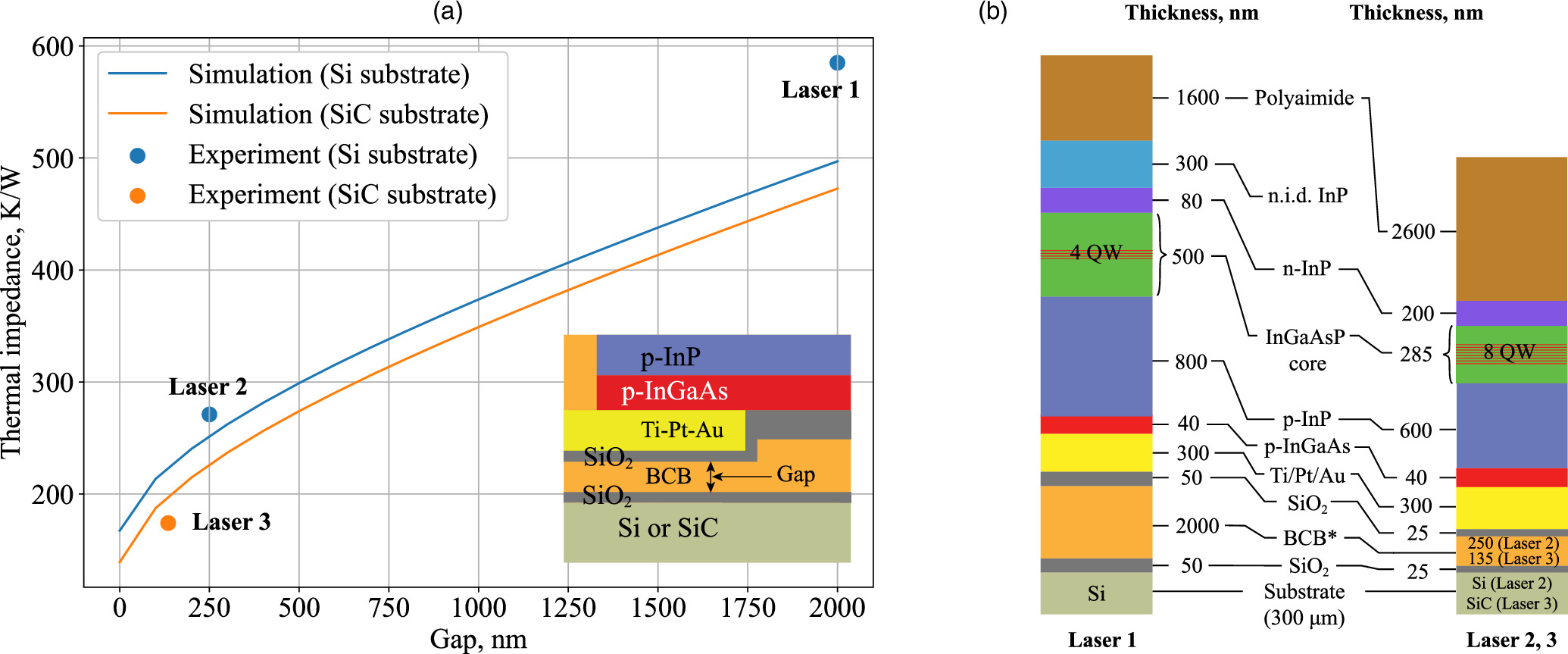
Fig. 2. (a) Thermal impedance simulation of a 500 μm DFB laser and experimental data for three lasers with the known gap. (b) Layer stack differences between the lasers used in the experiment. BCB* thickness is given as measured (Laser 2, 3) or estimated (Laser 1) directly below the laser contact metal.
Download figure:
Standard image High-resolution imageIn Fig. 2(b) we show the differences in the layer stack between three lasers, for which the experimental data is available. Note that in the experimental data, the value of the gap is known exactly for the lasers with a small gap (Laser 2 and 3). In contrast, for the laser with the large gap (Laser 1), the value is based on reflectometer measurements of cured BCB on a dummy sample and might be different for the measured device, which can explain the discrepancy with the model. Another part of the discrepancy might be coming from the differences in the layer stack. The wafers might also have a bow of up to 2 μm, which can also lead to an inefficient heat sinking and variation of thermal impedance across the wafer area.
Reducing the thickness of the BCB layer as spun on the wafer has limitations. Examples of bonding of a die 25) with 25 nm thick BCB or a 4 × 4 mm garnet 26) with 125 nm thick BCB were demonstrated previously. However, in practice, it is highly challenging to achieve a defect-free bonding of a non-planar 3 inch wafer when using BCB thickness equal to or less than the maximum step height in the wafer topography. The main sources of the bonding defects are hard particles landing on the wafer after the BCB spinning, and air bubbles that can appear between the two wafers due to the initial non-uniformity of the BCB layer when it is spun on a complex topography.
A unique property of the BCB is the way it changes its viscosity at different temperatures. As described in Ref. 27, after soft-baking at 100 C the viscosity is on the order of 105 Poise, however as the temperature goes up, the viscosity reduces, achieving a minimum of ≈1000 Poise at 170 C, after which it increases again due to increasing cross-linking. The bonding process starts at RT, when the BCB is highly viscose, however during the processing there is a stage when the viscosity drops, and the BCB can efficiently reflow. If at this moment pressure is applied to structures immersed in the BCB, these structures will naturally sink down and reach the bottom of the BCB layer. This effect has been demonstrated before in Ref. 28, where the authors used it to fabricate anchors preventing wafers from sliding against each other during the bonding process. In our experiment, we fabricate laser mesas as free-standing pillars, and we use the thickness of the BCB, which on a flat wafer would be equal to the laser mesa height. When the BCB reaches the low viscosity point, the pressure is applied, the BCB reflows, and we achieve an effective reduction of the BCB thickness under the laser mesa.
Another important aspect is the optimization of the wafer topography. We remove the thick p-doped InP from everywhere on the wafer surface, except from the area with laser mesas, which only takes 3.3% of the total wafer area. The rest of the devices on the wafer, such as passive waveguides and splitters, do not use this layer. This way we create regions, where excess BCB in a liquid form can be redistributed under pressure from the devices during the reflow step. Thus, contamination particles up to the size of the topography step height (in our case ≈1 μm) can be tolerated in those regions since the liquid BCB will surround the particles and planarize around them. Also, the air-filled voids that can appear in those regions due to topography variations will not affect the device's performance. At the same time, a very thin layer of BCB can be achieved between the actual devices and the substrate, creating an efficient path for heat extraction. This process is schematically shown in Fig. 3(a).
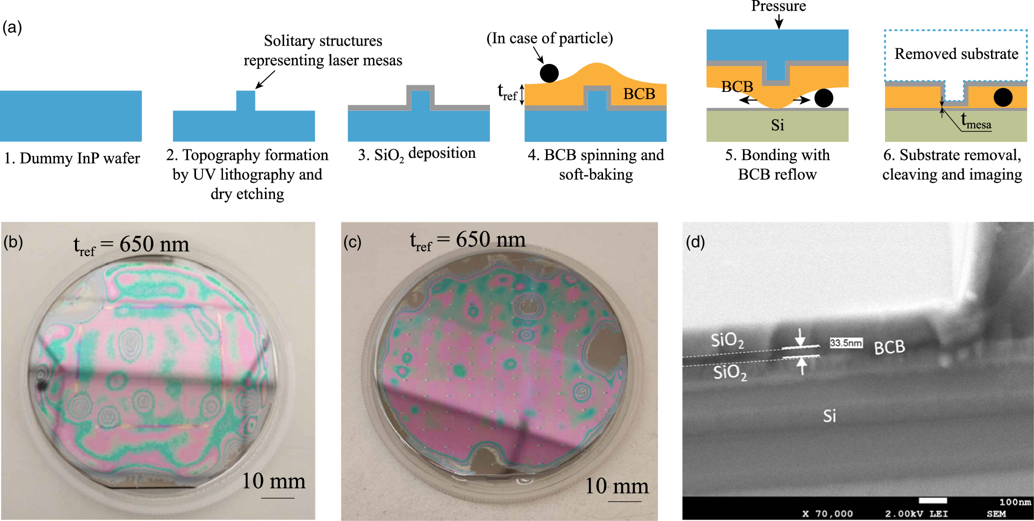
Fig. 3. (a) Process flow of experiments on 3 inch dummy wafers (experiments 1–3). The particle is not part of the process flow. (b)–(c): photographs of bonded dummy InP wafers after the substrate removal. (b): dummy InP with dense topography. (c): dummy InP with sparse topography. (d): SEM image of the cross-section of dummy wafer with sparse topography and metallization, bonded with tref = 650 nm.
Download figure:
Standard image High-resolution imageTo validate the process, we performed several experiments on dummy 3 inch InP wafers without epitaxial layers, and later on three 3 inch wafers with epitaxial layers. The process flow of experiments on dummy InP is shown in Fig. 3(a). To describe the experiments further, the following terminology will be used: tref (nm) is the reference BCB thickness, which we can measure with a reflectometer after spinning and soft-baking the BCB on a plain wafer. tmesa (nm) is the resulting BCB thickness between the mesa and the Si substrate after bonding (by "mesa" we mean a topography element that has the biggest step height above the wafer surface level). In all experiments we used the following flow: firstly, the topography was created on a wafer using UV or DUV lithography and dry etching. Secondly, a layer of SiO2 was deposited using plasma-enhanced chemical vapor deposition, the wafer was bonded to the Si substrate using BCB, and the InP substrate was removed using HCl. Finally, we cleaved the resulting Si wafer with BCB and SiO2 and imaged the cross-section in a scanning electron microscope (SEM) in the region, where the topography was on the original InP wafer to measure tmesa.
Experimental results are presented in Figs. 3(b)–3(f). In experiment 1, we used a dummy 3 inch InP wafer and UV mask with "dense" topography (the pattern consisted of 30 μm wide and 1 cm long lines separated by 120 μm and occupying approximately 10% of the wafer's total area) and tref = 650 nm. The photograph of the Si wafer with BCB and SiO2 after substrate removal is shown in Fig. 3(b). In experiment 2, we used the same tref = 650 nm, however, this time we used the same optical mask that was later used in the fabrication of wafers with actual devices, thus creating a "sparse" topography, since laser mesas are much smaller than the wafer area. The etching depth was identical to the mesa height of real lasers. On the real wafer, laser mesas occupy approximately 3.3% of the wafer surface, while the rest of the p-doped InP is etched away. With the sparse topography, on a dummy wafer tmesa = 33 nm was achieved, as measured on the cross-section in SEM [Fig. 3(d)]. In experiment 3, the same tref = 650 nm was used and the same mask, however this time we also deposited and lifted off Ti/Pt/Au (25-75-200 nm) in the laser contacts area, thus creating a topography that is almost identical to the topography of actual device wafers.
In Figs. 3(b)–3(c) bonding defects are visible. These defects are highly correlated to the initial contamination and quality of the used dummy wafers, which the cleaning procedure could not tolerate. Another source of the defects is that the BCB thickness (tref) was too thin to effectively planarize the full wafer surface, leading to air gaps close to the topography regions.
Once the BCB thickness was calibrated on dummy samples, we used the adjusted BCB thickness to bond wafers with real devices. The first wafer was bonded using tref = 750 nm, and after the fabrication was finished, we measured tmesa = 80 nm [red star in Fig. 4(c)]. The bonding defects were minor, however, the lasers on this wafer did not perform due to other fabrication errors at the post-bonding steps. The next wafer was bonded to Si using tref = 1100 nm. The photograph of this wafer after substrate removal is shown in Fig. 4(a). The laser cross Sect. was studied using a focused ion beam (FIB) cut to obtain the value of tmesa = 250 nm [also shown in Fig. 1(c)]. On this wafer, laser performance was measured (Laser 2 from Fig. 2 and later). Finally, we bonded a wafer with devices to the SiC substrate, using tref = 950 nm [Fig. 4(b), brown encircled star in Fig. 4(c)]. On this wafer, tmesa = 135 nm was measured by a profilometer using process control structures. The laser from this wafer was also characterized (Laser 3 from Fig. 2 and later). As visible from Figs. 4(a), 4(b), in both cases tref = 1100 nm and 950 nm, defect-free bonding is achieved. The structures visible on the wafer surface are n-contact metal pads of lasers, which were deposited before bonding. Figure 4(e) represents the summary of the relation between tref and measured tmesa. We find, that the actual topography plays a big role in the tmesa value, and therefore the tref must be carefully calibrated before bonding a wafer with devices.
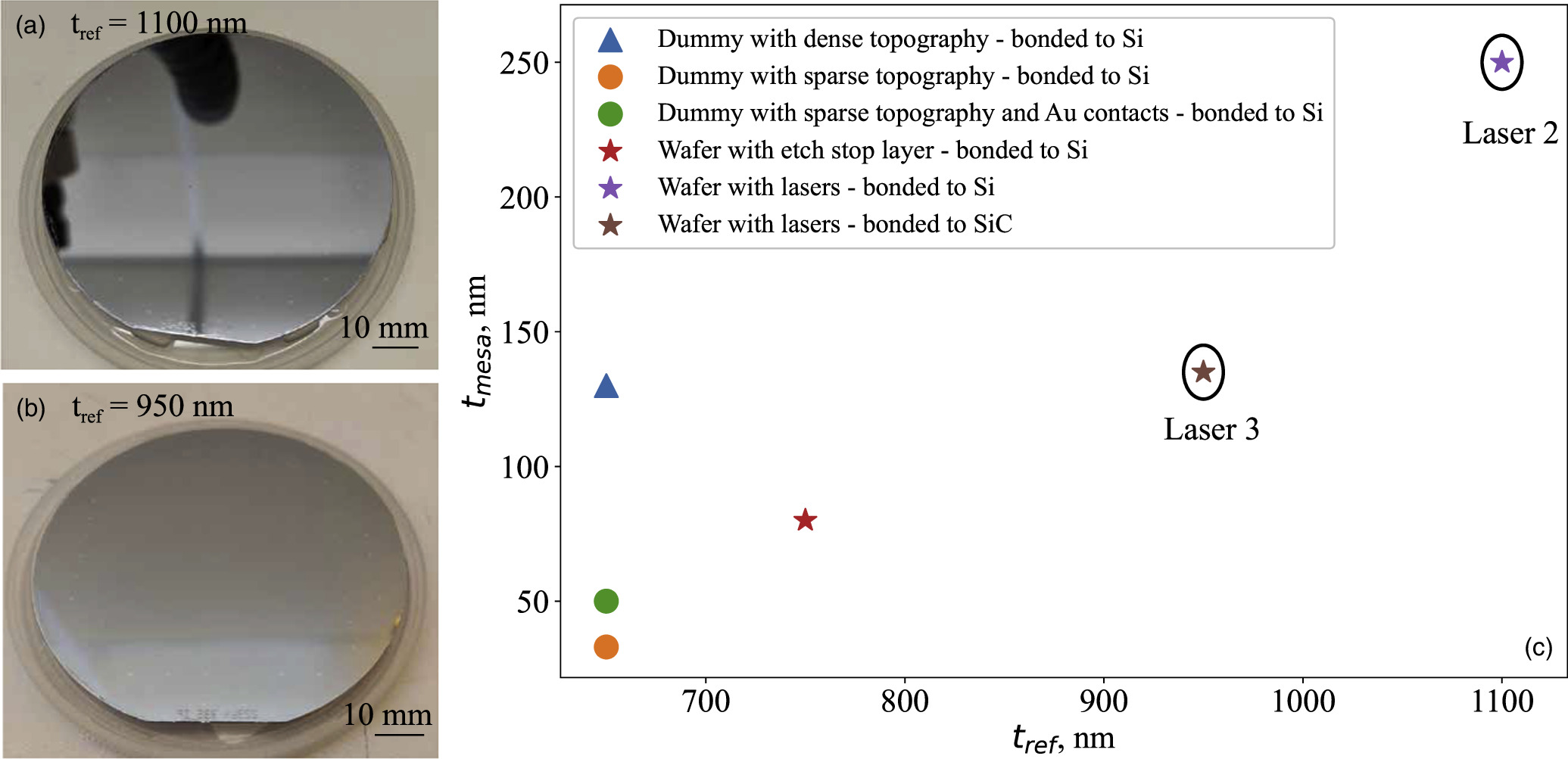
Fig. 4. (a)–(b) Bonded 3 inch wafers with laser structures after InP substrate removal. The top layer is the InP membrane. Bonded to: (a) Si, Laser 2 was measured on this wafer; (b) SiC, Laser 3 was measured on this wafer. (c): BCB thickness under the mesa, measured for different wafer topography and different reference BCB thickness. Measured wafers with devices are encircled.
Download figure:
Standard image High-resolution imageWe compare the thermal impedance of a laser fabricated previously with the non-optimized topography, no BCB reflow, and thick BCB (Laser 1), and lasers, fabricated with the new process and bonded to Si (Laser 2) and SiC (Laser 3). The differences in the layer stack between Laser 1 and Laser 2, 3 were shown in Fig. 2(b), and the differences in processing and topography are illustrated in Fig. 5. In the case of Laser 1, laser mesas were defined by trenches in the p-InP [Fig. 5(a), step 2], and tref = 2000 nm was used. Lasers 2 and 3 were fabricated with the new method and using tref = 1100 nm and 950 nm. At the step of mesa definition, we use an ArF scanner deep UV lithography with a dark field mask to remove p-InP from most of the wafer surface and only leave sparse free-standing mesas [Fig. 5(b), step 2]. The height of the mesa is 1 μm, which is equal to the chosen thickness of the p-InP layers plus the p-contact metal stack (Ti–Pt–Au). As was shown in Fig. 4, with this topography, a defect-free bonding can be achieved if the tref ≥ 950 nm. In the case of both wafers, the BCB is only spun on the InP wafer (Fig. 5, step 3). After spinning and soft-baking the BCB covers the topography non-uniformly. During the bonding process, firstly the InP wafer is brought into contact with the Si wafer at RT, then both wafers are secured by bonding glass on a holder and placed inside the bonding tool. The principal differences in the bonding process are listed in Table I and illustrated in Fig. 5, step 4. Inside the tool, the temperature is slowly ramped, a pressure of 700 N is applied from a piston, and the temperature is ramped again to 280 C and stays at this level for 1 h. After 1 h, the BCB is fully cured, the wafer sandwich is cooled down, extracted from the bonding tool, and the InP substrate is dissolved in HCl, leaving the bonded membrane (Fig. 5, step 5). After that, n-side mesa and gratings are defined, the semiconductor is etched away from contact pads, the wafer is planarized and finally, the top contact metals are deposited (Fig. 5, step 6). The fabrication process of the wafer with Laser 1 is similar, except that the waveguides are defined after bonding in the non-intentionally doped InP layer [Fig. 5(a), step 6].
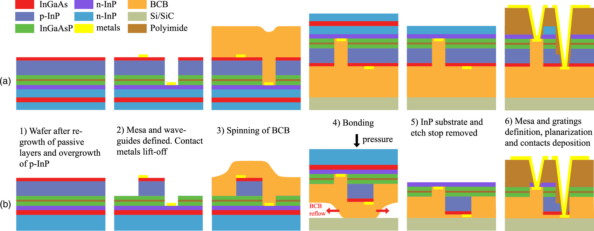
Fig. 5. Schematic fabrication process flow of IMOS lasers. (a) The process that was used for fabrication of Laser 1, thick BCB. (b) New process with reflow and optimized topography, used for fabrication of lasers 2 and 3. The SiO2 layer, which is used for passivation (thickness 100 nm) and BCB adhesion (thickness 50 nm for Laser 1, 25 nm for Laser 2 and 3), is omitted.
Download figure:
Standard image High-resolution imageTable I. Bonding process comparison for wafers used in the thermal impedance measurement experiment.
| Process parameters | Laser 1 | Laser 2 | Laser 3 |
|---|---|---|---|
| Substrate for bonding | Si | Si | SiC |
| Adhesion layer thickness (nm) | 50 | 25 | 25 |
| Reference BCB thickness (nm) | 2000 | 1100 | 950 |
| 1st ramp temperature (C) | 50 | 120 | 140 |
| Contact force (N) | 700 | 700 | 700 |
| 2nd ramp temperature (C) | 280 | 280 | 280 |
3. Results and discussion
We measured the thermal impedance of the three lasers to confirm, that the new bonding process improved the performance. All lasers are DFB of the same length (500 μm) and cross-section width (2 μm). All lasers were measured with an entire wafer lying on a copper chuck, while a water cooler and Peltier element ensured the substrate temperature control. First, we measured laser performance under continuous current injection, the chuck temperature was set at 10 °C in all cases. CW light–current–voltage characteristic (LIV) of Laser 1 and 2 is shown in Fig. 6(a). Note, that grating coupler losses were subtracted from data for both lasers. The threshold current of the Laser 1 was 36 mA, while for Laser 2, it was 26 mA. In Fig. 6(b), the spectra of Laser 2 for different driving currents are shown. To measure the thermal impedance, we use the technique described in detail in Ref. 14. In the steady state above the threshold, the thermo-optical effect (change of refractive index inside the active region due to Joule heating) causes the effective index of the mode to change, while the pitch of the DFB grating stays the same. Since the lasing wavelength is determined by the Bragg condition (DFB pitch times mode effective index), this leads to the wavelength shift proportional to the injected power. The lasing wavelength was measured as a function of dissipated power, which was calculated as IV − Poptical, where I is the driving current, V is the measured voltage across the diode, and Poptical is the measured optical power, corrected for the measured grating coupler losses. This measurement is illustrated in Fig. 7(a). Then laser spectra were measured in the pulsed current mode, where the frequency and duty cycle of pulses were chosen so that increasing current did not lead to wavelength shift (which means no self-heating). In this case, the wavelength shift is purely determined by the temperature of the wafer stage. The results are shown in Fig. 7(b). The data is then fitted with a linear function, and the thermal impedance is calculated as Zt [K/W] = (d λ/dP)/(d λ/dT).
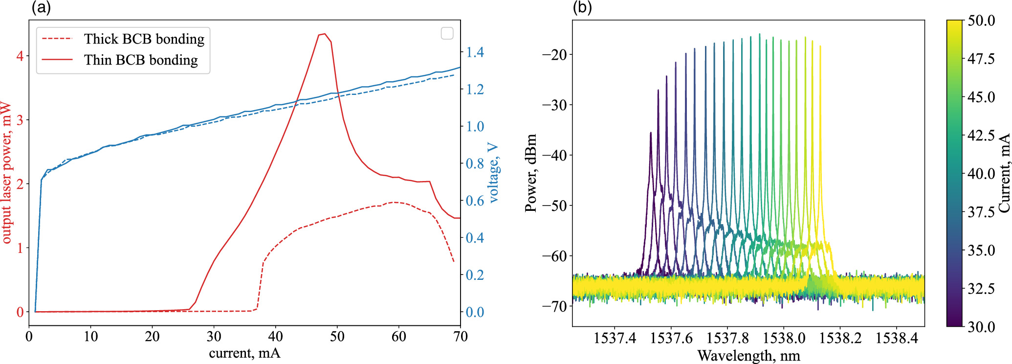
Fig. 6. (a) LIV for lasers bonded with 2 μm BCB (Laser 1) and 1100 nm BCB (Laser 2). The data is corrected for grating coupler losses. (b) Spectra of the Laser 2 versus different driving currents.
Download figure:
Standard image High-resolution image
Fig. 7. Lasing wavelength shift (a) relative to the threshold value for different dissipated powers in the CW regime and (b) relative to the value at 10 °C for different stage temperatures in the pulsed injection regime. Laser 1: non-optimized topography, bonded on thick BCB to Si. λ1 = 1560 nm at the threshold. Laser 2: optimized topography, reflow, bonded to Si. Laser 3: optimized topography, reflow, bonded to SiC. λ2,3 = 1537 nm at the threshold.
Download figure:
Standard image High-resolution image
We notice from Fig. 7(a), that for Laser 2 at higher currents, the wavelength shift vs dissipated power deviates from the linear function. This can be explained by the fact, that at 42 mA of injected current the laser hops to a different mode which has a slightly different effective index, and therefore the wavelength shift determined by the Bragg condition becomes smaller. This adds a source of uncertainty to the determination of the absolute value of the thermal impedance. If the whole range of measurement points is fitted with a linear function, Zt = 347 K W−1, and in the range from 42 to 50 mA, it is 271 K W−1. Laser 3 has Zt = 174 K W−1. A figure of merit (FOM) often found in the literature is thermal impedance normalized to the laser length. We find, that for Laser 2 (bonded to Si) it is 135 500 K/W*μm and for Laser 3 (bonded to SiC) it is 87 000 K/W*μm. Moreover, we measured Zt L = 63 600 K/W*μm for a 300 μm long DFB laser bonded to SiC. In Ref. 17, Zt L = 79 200 K/W*μm was reported for the case of BCB-free surface activated bonding of a flat wafer to Si. The best values, reported for heterogeneously integrated lasers, are 30 000 K/W*μm for flip-chip bonding of III–V laser on SOI 29) and 20 000 K/W*μm for a micro-transfer printed laser on bulk Si. 30)
When it comes to the short lasers, the thermal impedance of a 100 μm long DFB laser was measured to be 1430 K W−1 on the wafer, bonded to Si, and 830 K W−1 on the wafer, bonded to SiC. This is comparable to membrane devices fabricated with bonding on BCB before, such as in Ref. 31, where 3400 K W–1 was demonstrated for a 50 μm long DFB laser bonded with BCB on Si. However, our work is the first one, where such a result was achieved on a 3 inch wafer scale with high-topography PICs.
4. Conclusions
We proposed and validated a novel heat sink fabrication technology directly resulting from the wafer bonding, suitable for wafers with complex topography, without the need for additional lithography and etch steps to create thermal shunts. To the best of our knowledge, 135 nm is the thinnest adhesive layer in the heat-sink region achieved on a 3 inch wafer scale for non-planar wafers. We demonstrate, that by tuning the BCB thickness and optimizing the wafer topography and the bonding process, it is possible to reduce the thermal impedance of a 500 μm long DFB laser from 585 K W−1 (on a membrane bonded to Si using thick BCB) to 271 K W−1 in the case of bonding to Si substrate and to 174 K W−1 in the case of SiC substrate. Our process flow is applicable for arbitrarily complex surface topography, does not require mechanical polishing, and can be implemented in a clean room with a relaxed tolerance to air particles. This result opens the path to the scalable fabrication of photonic membrane lasers with low thermal impedance, integrated in complex opto-electronic circuits.
Acknowledgments
This work was supported by the Huawei research grant HDMI. The wafer fabrication was fully performed in the Nanolab @ TU/e facilities.