
Abstract
Sc-based contacts to Si:P have shown great potential for NMOS devices. However, the promising properties of this material system are not yet fully understood. This work provides new insights into the crystallinity and composition of annealed TiN/Sc/Si:P stacks. After silicidation, two distinct phases are evidenced, with orthorhombic ScSi lying atop a thin Sc1−x−ySixPy interfacial layer that shares a commensurate interface with the underlaid Si:P, hypothetically resulting in a low interface defectivity. The formed ScSi phase is observed to be thermally stable between ∼450 °C and 700 °C, which is suitable for most device applications. The impact of additional thermal budgets within this temperature range is investigated, revealing potential origins for thermally induced degradation of the contact properties.
Export citation and abstract BibTeX RIS
1. Introduction
Due to the extreme downscaling of today's high-end CMOS transistors, parasitic resistances play an important role in device performance. For small dimensions, one of the dominant contributions to the access resistance is the contact resistance (Rc = ρc/Ac) between the metal and the semiconductor in the source/drain (SD) regions of the devices. 1,2) Further performance improvements, enabled by higher drive currents using e.g. high-mobility channels, require reductions in contact resistance. 3) In addition to expanding the contact area Ac by engineering the shape of the contacts and by using conformal metal deposition techniques, 4) this can be achieved by lowering the contact resistivity ρc. 5) Minimizing this specific resistivity between the SD region and the contact metal (silicide) has now become a major objective. 6,7)
In recent years, significant progress has been made and aggressive performance levels, enabled by novel material systems and process options, were reported. 8) For the rapid assessment of contact properties, Yu et al. introduced multi-ring circular transmission line model (MR-CTLM) structures which combine a simple fabrication process with high ρc extraction accuracy. 9,10) Using these novel test structures, it was demonstrated that, despite a reduced Schottky barrier height (SBH), metal/insulator/semiconductor (MIS) contacts do not outperform their metal/semiconductor (MS) counterparts in terms of ρc on highly doped n+-Si. 10,11) This led to the conclusion that, beyond an active doping concentration of 3 × 1020 cm−3, the SBH no longer is the dominant parameter determining ρc. Instead, for highly doped semiconductors, the conduction across the MS interface is dominated by tunnelling-based carrier transmission. 12) As the insulating interface of MIS contacts results in a reduction in tunnelling probability, MIS contacts were concluded not to be compatible with the needs of advanced CMOS transistors. Instead, advanced contacts usually rely on heavily doped SD layers contacted with Ti. 8) For example, utilizing a pre-contact amorphization implantation (PCAI) Ti silicidation technique, Yu et al. 10,12) demonstrated ultralow ρc down to (1.3–1.5) × 10−9 Ωcm2 for TiSix alloys contacting highly doped n+-Si (phosphorous (P) chemical concentration of 3 × 1020 cm−3). The PCAI-induced low contact resistivity was attributed to an enhanced Ti silicidation, causing the formation of interfacial TiSix crystallites between an amorphous TiSi alloy and Si. An alternative approach, reported by Ni et al., 13) which utilizes either a plasma or beam line (cryogenic) implant followed by a laser anneal, was demonstrated to show a similarly low contact resistivity (down to 1.2 × 10⁻⁹ Ωcm2) for Ti/Si:P. The implantation and subsequent anneal were shown to result in an enhanced dopant activation and a promoted epitaxial regrowth of the Si:P SD, leading to the exceptionally low contact resistivity observed.
In view of these learnings, novel low temperature (; LT, T < 500 °C) epitaxy processes have been developed. 14) In addition to their compatibility with modern device architectures that require limited thermal budgets, such as e.g. complementary FETs, 15,16) they enable active doping concentrations exceeding 1 × 1021 cm−3. Rosseel et al. 17) demonstrated contact resistivities down to 2 × 10⁻⁹ Ωcm2 by combining LT Si:P with Ti contacts without any post deposition treatments. In addition to the experimental progress made on contacts in the last years, there have been several studies reporting on the fundamental limitations of the contact resistivity, 6,18,19) which highlight the importance of the effective mass of the majority charge carriers, Fermi energies and density of states in k-space of the metal and semiconductor.
Inspired by these insights, Porret et al. screened exploratory contact metals and reported on Sc contacts to LT Si:P clearly outperforming their Ti counterparts, with a contact resistivity ρc down to ∼1.3 × 10⁻⁹ Ωcm2. 8) This corresponds to a ∼35% decrease compared to Ti/LT Si:P. This improvement in contact resistivity was hypothetically attributed to (i) the formation of a highly crystalline scandium monosilicide (ScSi), (ii) the presence of a P-rich Sc1−x−y Six Py interfacial layer and (iii) the gettering of oxygen towards the top of the Sc-rich layer. However, the origin for this performance boost is not yet understood. The current study therefore focuses on the fundamental assessment of the interface composition and the crystalline properties of blanket TiN/Sc/Si:P contact stacks subjected to various annealing treatments. The final goal is the identification of the origins of the good contact properties observed for this system after thermally induced solid state reactions. To the best of the authors' knowledge, only one report has been published about the reaction of Sc thin films with Si. Thomas et al. 20) evidenced the formation of two different silicides as a result of a solid state reaction between Sc thin films and Si(001) substrates. They concluded that an orthorhombic ScSi phase forms at a temperature of about 500 °C. The corresponding reaction was presumed to be diffusion controlled. At higher temperatures (about 900 °C), the nucleation-controlled formation of hexagonal ScSi1.7 was observed.
This manuscript is an extended version of the recent work published in Ref. 21, which focused on TiN/Sc/Si:P contact stacks subjected to a limited thermal budget ("sinter annealing," i.e. 20 min at 420 °C in H2/N2). It provides novel insights (thanks to additional energy dispersive X-ray spectroscopy (EDS) and grazing incidence X-ray diffraction (GI-XRD) measurement results) regarding the properties of this system after sinter annealing. Additionally, due to the relevance of higher thermal budgets for some device applications, this manuscript also reports on the impact of higher temperature anneals. These additional treatments are referred to as post metal anneal "PMA" and dynamic random-access memory anneal "DRAM anneal" in the following (corresponding to a thermal budget of 30 min at 525 °C and 4 h at 650 °C, respectively). The latter is of particular importance for memory applications as the contacts used in these devices have to withstand significantly higher thermal budgets compared to conventional logic devices (typically 600 °C–750 °C, >1 h). 22) These high thermal budgets are required to ensure that the capacitors in a DRAM cell have a sufficiently long charge retention time. 23)
2. Experimental methods
2.1. Sample fabrication
The contact stacks consist of three layers [schematically depicted in Fig. 1(a)]: an epitaxial S/D layer grown on p-Si(001), a contact metal and a capping layer/liner (which prevents oxidation of the underlying contact metal). The bottom layer is highly P-doped Si (Si:P) containing 3% of P. It is grown by low temperature reduced pressure CVD, according to the process reported by Rosseel et al. 14) Immediately before the contact deposition, a wet etch in diluted HF is performed to remove the Si(:P) native oxide., 24,25) Sc contacts (nominally 15 or 25 nm thick) are then deposited at RT by physical vapor deposition (DC sputtering). The capping layer consists of TiN (10 nm thick), which is deposited by reactive sputtering of Ti with N2. The deposition of the contact metal and TiN capping layer are performed without vacuum break. These contact stacks were deposited on both blanket and MR-CTLM patterned wafers, allowing various characterization techniques and contact resistivity measurements. For the MR-CTLM patterned wafers, a finishing metal stack consisting of Cu/TaN/Ta is added. 8,9) Note that the TaN only contains 10%–20% N. Finally, the samples are annealed in forming gas (10% H2) for 20 min at 420 °C (referred to as "sinter anneal" in the following). Two additional PMA treatments are considered: (i) a logic PMA at 525 °C for 30 min (referred to as "PMA" in the following) and (ii) a DRAM anneal at 650 °C for 4 h (referred to as "DRAM anneal" in the following). Both annealing treatments are conducted in N2 atmosphere. Note that the samples subjected to these anneals are also sinter annealed afterwards. Figures 1(b)–1(d) schematically depict the different situations considered in the work.
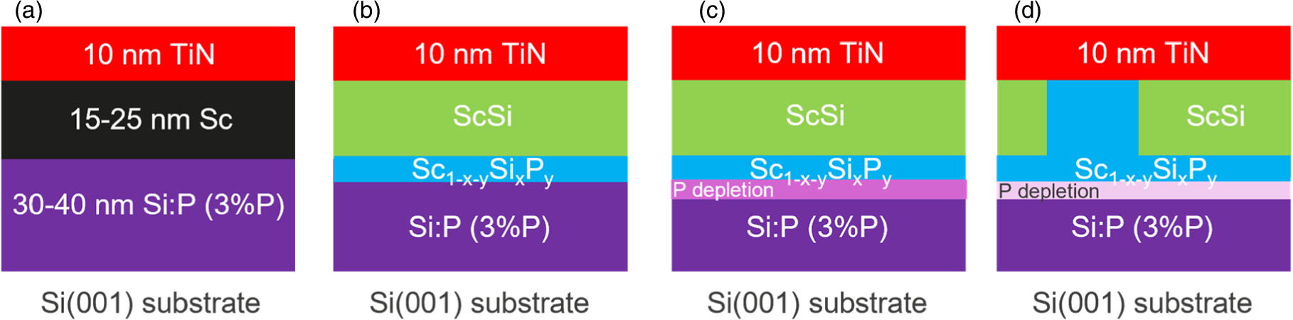
Fig. 1. Schematic illustration of the contact stack (a) as deposited, (b) after sinter anneal (20 min at 420 °C), (c) after PMA at 525 °C for 30 min and (d) after DRAM anneal (4 h at 650 °C). Note that the latter two samples were also subjected to sinter annealing at end of process.
Download figure:
Standard image High-resolution image2.2. Physical characterization
Cross section transmission electron microscopy (TEM) inspections were performed on MR-CTLM patterned wafers to investigate the structural properties across contact interfaces. These were conducted using a Titan3 G2 60–300 (FEI) system operated at 200 kV. Complementary EDS measurements were used to extract composition profiles throughout the contact stack. Note that such measurements are prone to significant quantitative errors that can arise due to e.g. the TEM specimen preparation, overlaps between different peaks characteristic of the probed elements and the lack of suitable standards. Additional physical characterizations were conducted on blanket duplicate samples. To gain further insight into the chemistry at different interfaces throughout the contact stack, X-ray photoelectron spectroscopy (XPS) analyses were conducted on blanket samples using a QUANTES instrument from Physical electronics equipped with a monochromatized photon beam of 1486.6 eV. This system is equipped with a monoatomic Ar sputter gun used for depth profiling by alternating XPS measurement cycles and Ar+ ion sputtering. This capability was utilized to measure XPS spectra at different locations throughout the TiN/Sc/Si:P contact stacks. Charge neutralization and energy calibration with respect to the C  peak at 284.8 eV, corresponding to adventitious carbon, were used.
26) It was verified that charge calibration with respect to the Si
peak at 284.8 eV, corresponding to adventitious carbon, were used.
26) It was verified that charge calibration with respect to the Si  core level spectrum
27) yields the same qualitative results.
core level spectrum
27) yields the same qualitative results.
XRD was used to assess the macro-scale crystalline properties of blanket samples. Specifically, in situ XRD, which records the XRD patterns as a function of annealing temperature during a slow temperature ramp (0.2 °C s−1) from RT to 900 °C in He(95%)/H2(5%) atmosphere, was used to assess the thermal evolution and stability of the formed phases. This was done using a Bruker D8 diffractometer with a Cu Kα X-ray source and a linear (1D) detector. These measurements are complemented by additional ex situ XRD measurements using a Bruker JVX diffractometer, enabling Bragg–Brentano θ–θ and grazing incidence XRD measurements.
3. Results and discussion
3.1. Results
3.1.1. Crystallinity and composition after sinter anneal
Figure 2(a) displays a high resolution annular bright field cross-section scanning TEM (HR ABF-STEM) image from a 10 nm TiN/25 nm Sc/30 nm Si:P contact stack after sinter anneal. Figure 2(b) shows a corresponding EDS line scan, measured across the TiN/Sc/Si:P stack. In addition to the Cu/TaN/Ta/TiN metal stack, three layers can be clearly distinguished: the epitaxial Si:P layer, a scandium monosilicide formed above it and a P-rich Sc1−x−y Six Py interfacial layer in the junction region [schematically shown in Fig. 1(b)]. The three layers are crystalline, as evidenced by the periodicity of the different lattice planes and through the associated fast Fourier transforms (FFT), shown as insets in Fig. 2(a).

Fig. 2. (a) HR ABF-STEM cross-section of a 10 nm TiN/25 nm Sc/40 nm Si:P contact stack after sinter anneal measured along the Si[010] zone axis. FFTs extracted from the indicated rectangular regions are added in insets (plotted on the same scale to allow comparison). (b) EDS line scan measured across the contact stack, along the Si[001] direction. Note that, as opposed to the other contact stacks studied in this work, this sample contained 25 nm of Sc as deposited. Despite this increase in thickness compared to the nominal 15 nm, the Sc layer is fully silicided after sinter annealing. Additionally, the thickness of the interfacial Sc1−x−y Six Py layer is not affected by this change.
Download figure:
Standard image High-resolution imageThanks to the monocrystallinity of the epitaxial Si:P layer, the corresponding reciprocal space pattern shows well-defined diffraction spots. This is not perfectly the case for the pattern corresponding to the Sc1−x−y Six Py region due to the limited thickness of this layer and the subsequent restricted area available for this analysis. As a result, no clear periodicity can be observed along the Si[001] direction. Despite this, one can observe a similar periodicity of the lattice planes in the Si[100] direction, suggesting the presence of a commensurate interface between the ScSi and the Si:P layers. The crystalline structure observed in the Sc1−x−y Six Py region is consistent with that of a cubic phase, wherein Si is partly substituted by P to better accommodate the interface lattice planes. Theoretical investigations regarding this specific crystalline phase are ongoing and will be the object of a future report.
Figure 3 shows the θ–θ XRD [Fig. 3(a)], exhibiting a main peak around 36°, and GI-XRD [Fig. 3(b)] patterns acquired on a duplicate blanket stack. Both measurements are consistent with the presence of orthorhombic ScSi (COD card no. 00-000-9969, mp-9969). Figure 4 compares the FFT extracted from the ScSi region of Fig. 2(a) with the theoretical diffraction pattern for this crystalline phase (in the [−101] zone axis).
28) The two patterns show reasonable agreement, confirming the presence of the orthorhombic ScSi phase. However, the ScSi appears to be tilted with respect to the Si[001] direction (approximately 9° tilt in the present case). Different tilts have been observed at different locations across the TEM specimen ( 9° tilts for twelve different locations), which indicates that the ScSi is polycrystalline. The presence of this tilted phase on larger scales has not been confirmed.
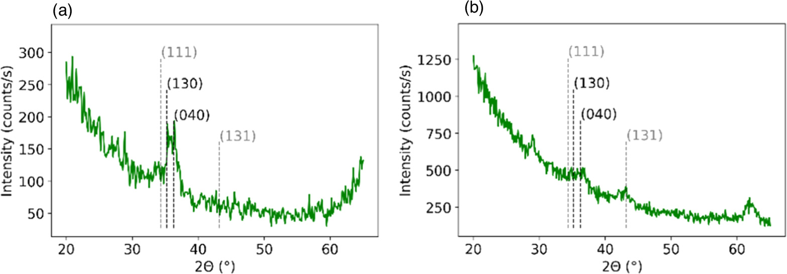
Fig. 3. (a) Bragg–Brentano θ–θ XRD and (b) GI-XRD pattern from a 10 nm TiN/15 nm Sc/40 nm Si:P contact stack measured after sinter anneal. The indicated peak positions correspond to orthorhombic ScSi (COD card no. 00-000-9969, mp-9969). The 2θ values corresponding to the (111), (130), (040) and (131) planes are 34.348°, 35.206°, 36.245° and 43.208°, respectively. Note that contributions may arise from the capping layer under the form of cubic TiN (COD card no. 00-000-0492, mp-492), which is expected to present peaks at 36.567°, 42.477° and 61.634° for the (111), (200) and (220) planes, respectively.
Download figure:
Standard image High-resolution image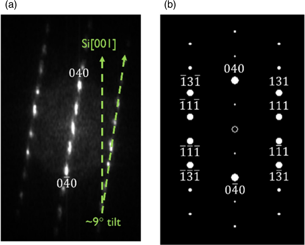
Fig. 4. Diffractograms (a) extracted from the ScSi region of the HR ABF-STEM image shown in Fig. 2(a) using FFT and (b) calculated theoretically for the [−101] direction as zone axis. 28)
Download figure:
Standard image High-resolution imageFinally, the ScSi/Si:P interface chemistry is investigated by XPS, in addition to EDS. Figure 5 shows the P  XPS core level spectra recorded at the ScSi/Si:P interface [Fig. 5(a)] and in the top part of the Si:P layer [Fig. 5(b)]. Both spectra are shown before and after sinter anneal. Additionally, the spectrum of a pristine blanket Si:P layer is shown as reference. At the ScSi/Si:P interface (i.e. in the Sc1−x−y
Six
Py
region), the sinter anneal induces a (∼1 eV) shift of the P
XPS core level spectra recorded at the ScSi/Si:P interface [Fig. 5(a)] and in the top part of the Si:P layer [Fig. 5(b)]. Both spectra are shown before and after sinter anneal. Additionally, the spectrum of a pristine blanket Si:P layer is shown as reference. At the ScSi/Si:P interface (i.e. in the Sc1−x−y
Six
Py
region), the sinter anneal induces a (∼1 eV) shift of the P  peak towards lower binding energies. Considering the electronegativity of the pertinent elements (Table I), it is proposed that this shift is due to the replacement of P–Si bonds by P–Sc bonds (this will be further studied in future works using e.g. synchrotron radiation). This observation is compatible with the incorporation of P atoms in the ScSi crystal lattice at this interface and subsequent formation of a ternary crystalline phase Sc1−x−y
Six
Py
. Note that no complementary peak shift was detected in the Si
peak towards lower binding energies. Considering the electronegativity of the pertinent elements (Table I), it is proposed that this shift is due to the replacement of P–Si bonds by P–Sc bonds (this will be further studied in future works using e.g. synchrotron radiation). This observation is compatible with the incorporation of P atoms in the ScSi crystal lattice at this interface and subsequent formation of a ternary crystalline phase Sc1−x−y
Six
Py
. Note that no complementary peak shift was detected in the Si  and Sc
  core level spectra (not shown). As shown in the work of Lee et al.,
29) the addition of a few percent of P in the Si lattice of an epitaxial Si:P layer does not result in a noticeable shift in Si
core level spectra (not shown). As shown in the work of Lee et al.,
29) the addition of a few percent of P in the Si lattice of an epitaxial Si:P layer does not result in a noticeable shift in Si  core level peak position. The same is expected to be true for the Sc
  core level spectra.

Fig. 5. XPS P  core level spectra (before and after sinter anneal) measured in a 10 nm TiN/15 nm Sc/40 nm Si:P contact stack (a) at the ScSi/Si:P interface and (b) in the top part of the Si:P layer. The spectra were recorded in these regions by XPS depth profiling. Throughout the depth profile, these two regions were identified as the measurement corresponding to the maximum P
  peak intensity and the measurement at which the Sc
  peak disappears (not shown), respectively. The P
  core level spectrum of a pristine Si:P layer is shown as reference.
Download figure:
Standard image High-resolution imageTable I. Electronegativity (EN) values and atomic radii (ra) of Sc, Si and P.
| Element | EN | ra (pm) |
|---|---|---|
| Sc | 1.36 | 230 |
| Si | 1.90 | 210 |
| P | 2.19 | 195 |
3.1.2. Thermal stability
The thermal stability of TiN/Sc/Si:P contact stacks is investigated by in situ XRD. Figure 6 shows the in situ XRD pattern for a contact stack consisting of 10 nm TiN/15 nm Sc/40 nm Si:P (3%P). One can observe the phase transition from metallic Sc (COD Card no. 00-060-1273, mp-601273 and COD Card no. 00-000-0036, mp-36, corresponding to hexagonal and cubic Sc, respectively) to the orthorhombic ScSi phase at ∼450 °C. In the ∼350 °C–450 °C range, no Sc-related peaks are observed, suggesting that the formation of the orthorhombic ScSi is preceded by the solid state amorphization of Sc. The orthorhombic monosilicide phase remains stable up to ∼700 °C. At higher temperatures, the phase is expected to transition towards hexagonal Si-rich scandium silicide ScSiz
with 1.7  z
z
 2.
20) The presence of this phase cannot be verified based on this measurement. This is due to a peak overlap between cubic TiN(111) (COD Card no. 00-000-0492, mp-492), potentially originating from the TiN capping layer, and hexagonal ScSiz
(101). Additionally, Fig. 6 evidences the formation of cubic Sc2O3 (COD Card no. 00-000-0216, mp-216) above 700 °C.
2.
20) The presence of this phase cannot be verified based on this measurement. This is due to a peak overlap between cubic TiN(111) (COD Card no. 00-000-0492, mp-492), potentially originating from the TiN capping layer, and hexagonal ScSiz
(101). Additionally, Fig. 6 evidences the formation of cubic Sc2O3 (COD Card no. 00-000-0216, mp-216) above 700 °C.
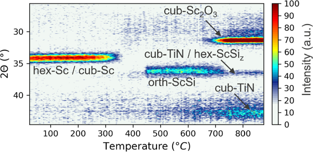
Fig. 6. In situ XRD pattern of a pristine 10 nm TiN/15 nm Sc/40 nm Si:P stack measured during a slow temperature ramp of 0.2 °C s−1 from RT to 900 °C in He(95%)/H2(5%) atmosphere.
Download figure:
Standard image High-resolution image3.1.3. Crystallinity and composition after logic and DRAM anneals
Next, the effect on the crystallinity and composition of an additional thermal budget within the temperature window where the orthorhombic ScSi is thermally stable is investigated. For this, two post-metal annealing treatments are considered, consisting of an anneal at 525 °C for 30 min and one at 650 °C for 4 h, referred to as "PMA" and "DRAM anneal," respectively.
Similarly to the sinter annealed sample, the structural properties are investigated by XRD and HR ABF-STEM. The stack composition is investigated by XPS and EDS. Figure 7 shows the θ–θ XRD patterns after these different annealing treatments. In agreement with the thermal stability window identified above, the orthorhombic ScSi phase remains present after the additional thermal budget. Unexpectedly, one observes an increase in peak intensity of the main peak corresponding to the orthorhombic ScSi phase. Given that the Sc is fully silicided after the sinter anneal (Fig. 2), it is not clear what this can be attributed to.

Fig. 7. Comparison between the Bragg–Brentano θ–θ XRD pattern for 10 nm TiN/15 nm Sc/30–40 nm Si:P subjected to different thermal budgets.
Download figure:
Standard image High-resolution imageThe HR ABF-STEM and EDS measurements after the PMA and DRAM anneals are shown in Figs. 8 and 9 (HR ABF-STEM shown at two different locations), respectively. The 525 °C PMA does not have a significant impact on the crystallinity [Fig. 8(a)] and composition [Fig. 8(b)], within the error bars of the measurement technique. Indeed, similarly as for the sinter annealed sample, one observes the presence of three distinct and highly crystalline layers [as schematically depicted in Fig. 1(c)]: the Si:P S/D, the Sc1-x-y Six Py interfacial layer and the ScSi (with slightly lower Sc concentration compared to the sinter annealed sample). In accordance with the XRD measurement shown in Fig. 7, the FFT of the region corresponding to the latter layer [upper inset of Fig. 8(a)] confirms the presence of the orthorhombic ScSi phase.
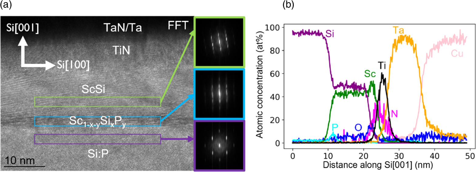
Fig. 8. (a) HR ABF-STEM cross-section of a 10 nm TiN/15 nm Sc/40 nm Si:P contact stack after PMA (30 min at 525 °C) acquired along the Si[010] zone axis. FFTs extracted from the indicated rectangular regions are added in insets (plotted on the same scale to allow comparison). (b) The corresponding EDS line scan measured along the Si[001] direction.
Download figure:
Standard image High-resolution image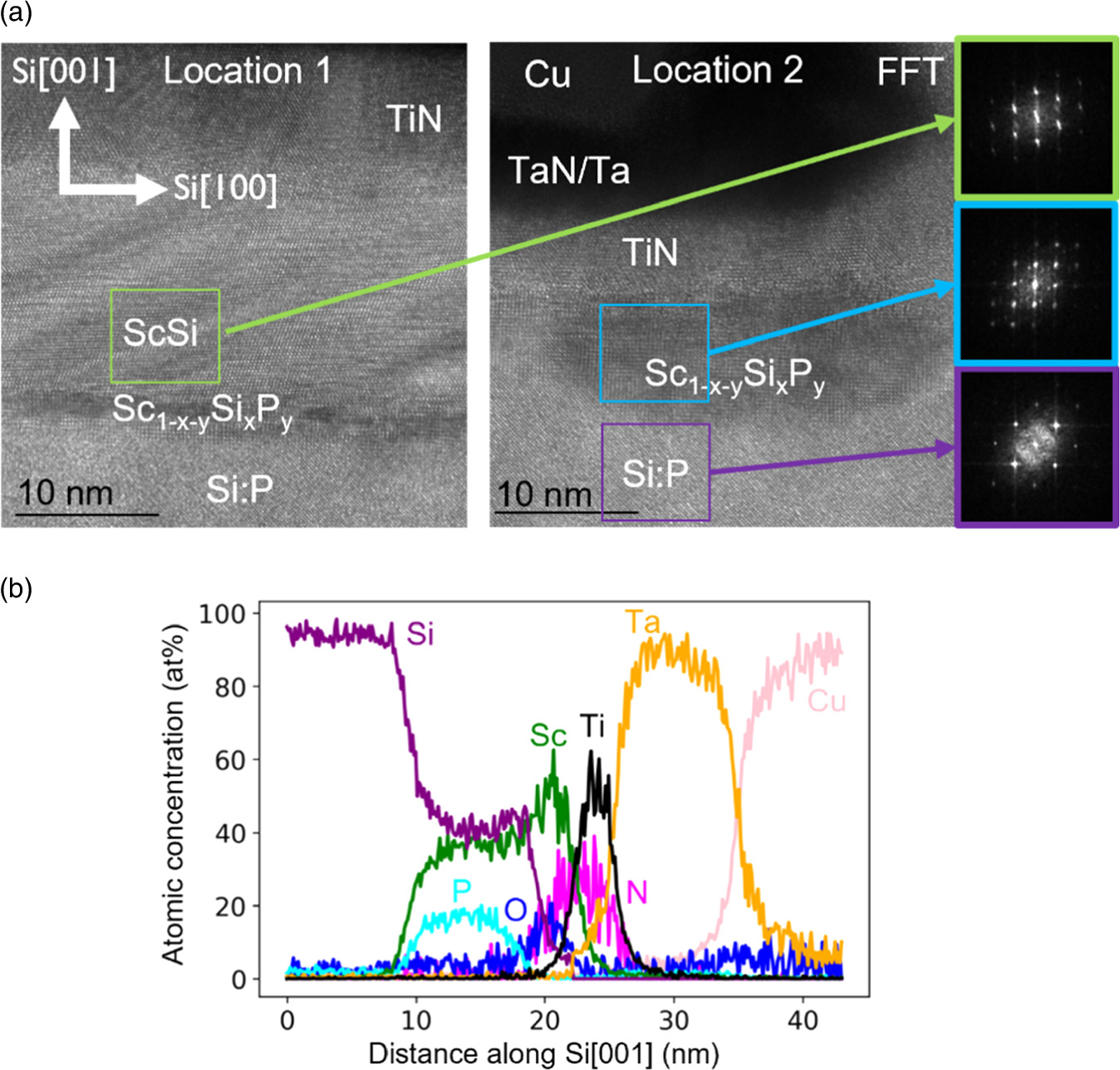
Fig. 9. (a) HR ABF-STEM cross-section of a 10 nm TiN/15 nm Sc/40 nm Si:P contact stack after DRAM anneal (4 h at 650 °C) acquired along the Si[010] zone axis at two different locations of the sample. FFTs extracted from the indicated rectangular regions are added in insets (plotted on the same scale to allow comparison). (b) The corresponding EDS line scan measured at location 2 along the Si[001] direction.
Download figure:
Standard image High-resolution imageAfter DRAM anneal, one however notices several changes compared to the sinter annealed sample. In some regions, the three layers outlined above are no longer visible [Fig. 9(a)] and the silicide is inhomogeneous in composition [Fig. 9(b)]. Local grains with significantly increased amounts of P ( 18%) can be observed [location 2 in Fig. 9(a)]. As shown by the FFT [middle inset in Fig. 9(a)], these local grains have a different crystalline signature compared to ScSi [upper inset in Fig. 9(a)]. It is hypothesized that this material corresponds to the cubic Sc1−x−y
Six
Py
phase described above. In some other regions [e.g. location 1 in Fig. 9(a)], the crystallinity and composition remain similar as observed for the samples that received a lower thermal budget and the different layers (Si:P, Sc1−x−y
Six
Py
and ScSi) remain well-defined. The difference between location 1 and location 2 in Fig. 9(a) evidences the presence of non-uniform interfaces and contact properties, which are assumed to be detrimental to the contact resistivity, in particular when contacts are formed on scaled devices.
18%) can be observed [location 2 in Fig. 9(a)]. As shown by the FFT [middle inset in Fig. 9(a)], these local grains have a different crystalline signature compared to ScSi [upper inset in Fig. 9(a)]. It is hypothesized that this material corresponds to the cubic Sc1−x−y
Six
Py
phase described above. In some other regions [e.g. location 1 in Fig. 9(a)], the crystallinity and composition remain similar as observed for the samples that received a lower thermal budget and the different layers (Si:P, Sc1−x−y
Six
Py
and ScSi) remain well-defined. The difference between location 1 and location 2 in Fig. 9(a) evidences the presence of non-uniform interfaces and contact properties, which are assumed to be detrimental to the contact resistivity, in particular when contacts are formed on scaled devices.
Figure 10 compares phosphorus EDS maps, which show the local relative phosphorous concentration, from TiN/Sc/Si:P interface regions for the sinter annealed [Fig. 10(a)], the PMA [Fig. 10(b)] and DRAM annealed [Fig. 10(c)] sample. Considering the EDS composition profiles shown above, the pertinent layers constituting the contact stack (Si:P, Sc1−x−y Six Py and ScSi) can be identified. As evidenced in Fig. 10(c), a local P-depletion [compared to the situation after only the sinter annealing depicted in Fig. 10(a)] in the Si:P near the Si:P/ScSi interface can be observed for the sample that received the additional DRAM annealing. The same holds true after the 525 °C PMA [Fig. 10(b)] but to a far lesser extent.
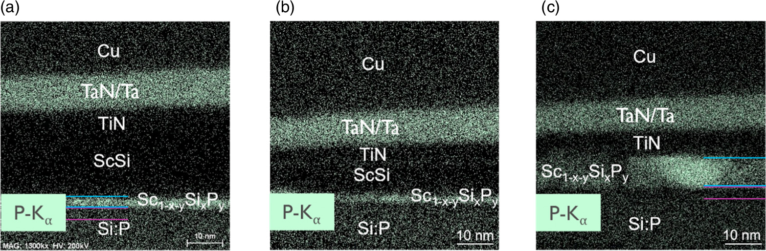
Fig. 10. Phosphorus EDS maps, showing the local relative phosphorous concentration, of 10 nm TiN/15–25 nm Sc/40 nm Si:P contact stacks (with Cu/TaN/Ta as finishing metal stack) after (a) sinter anneal, (b) PMA and (c) DRAM anneal. Note that the region of high intensity labelled as TaN/Ta is due to an overlap between the P- and Ta-
 peaks. Hence, it does not correspond to the actual presence of P in these areas. Horizontal lines are included to materialise boundaries between different layers.
Download figure:
Standard image High-resolution imageThe depletion of phosphorus in the epitaxial Si:P layer is further investigated by XPS. Figure 11 compares the XPS P  core level spectra for different thermal budgets measured at the P-rich interfacial layer [Fig. 11(a)] and in the top part of the Si:P layer [Fig. 11(b)]. One observes an increase in the relative intensity of the P
  peak compared to the background (which is dominated by a Si plasmon loss peak
30)) due to the additional thermal budget. This is indicative of an increased P concentration in the interfacial region caused by the additional annealing step and is therefore in accordance with the phosphorus EDS maps (Fig. 10). Note also that the peak positions of the P
peak compared to the background (which is dominated by a Si plasmon loss peak
30)) due to the additional thermal budget. This is indicative of an increased P concentration in the interfacial region caused by the additional annealing step and is therefore in accordance with the phosphorus EDS maps (Fig. 10). Note also that the peak positions of the P  core level spectra align for the three different thermal budgets, which is consistent with the presence of P–Sc bonds outlined above.

Fig. 11. Comparison between the XPS P  core level spectra for different thermal budgets measured in a 10 nm TiN/15 nm Sc/40 nm Si:P contact stack (a) at the ScSi/Si:P interface and (b) in the top part of the Si:P layer. The spectra were recorded in these regions by XPS depth profiling. Throughout the depth profile, these two regions were identified as the measurement corresponding to the maximum P
  peak intensity and the measurement at which the Sc
  peak disappears (not shown), respectively.
Download figure:
Standard image High-resolution image
Remarkably, chemical quantification using XPS results in the same P concentration in this region for the PMA and DRAM annealed samples (both ∼6%). This result seemingly contradicts the data shown in Figs. 8(b) and 9(b), which shows significantly higher P concentrations for the sample subjected to the higher thermal budget. This can be understood by considering that the chemical concentration as determined by XPS is a spatial average across an area in the order of ∼1 μm2, while EDS provides local (∼1  m2) information. This indicates that the DRAM anneal causes a redistribution of the P present in the Si:P and Sc1−x−y
Six
Py
, leading to the formation of regions with significantly higher P concentrations and regions with lower P contents. This results in a spatially inhomogeneous silicide and the loss of the distinct Sc1−x−y
Six
Py
and ScSi layers which yield a remarkably low contact resistivity.
m2) information. This indicates that the DRAM anneal causes a redistribution of the P present in the Si:P and Sc1−x−y
Six
Py
, leading to the formation of regions with significantly higher P concentrations and regions with lower P contents. This results in a spatially inhomogeneous silicide and the loss of the distinct Sc1−x−y
Six
Py
and ScSi layers which yield a remarkably low contact resistivity.
3.2. Discussion
3.2.1. Origin of the promising contact properties achieved after sinter anneal
The results shown above indicate that the sinter anneal fully silicides the Sc layer and forms orthorhombic ScSi. This silicide phase is observed to be locally tilted with respect to the Si[001] direction. The presence of this tilted phase on larger scales has not been confirmed. However, the comparison of the θ–θ and GI-XRD patterns (Fig. 3), which probe the out-of-plane and in-plane crystalline periodicity to a different extent, indicates that the orthorhombic ScSi is textured with its (130) and (040) planes preferentially oriented parallel to the Si(001) planes. These results, in addition to the tilted ScSi grain observed in Fig. 4(a), encourage further studies on the texture of this material.
In addition to the orthorhombic ScSi, a thin crystalline P-rich interfacial layer between the ScSi and Si:P is formed. The formation of this layer as observed in HR ABF-STEM and EDS is consistent with XPS results on blanket duplicate samples which shows that, at this interface, the sinter anneal causes a partial replacement of P–Si bonds (originally present in the Si:P layer) by P–Sc bonds. This is compatible with the incorporation of P in the ScSi lattice and the formation of an interfacial crystalline ternary compound Sc1−x−y Six Py . Considering the atomic radius of these elements (Table I), this is expected to decrease the lattice constant compared to ScSi, bringing it close to that of Si:P and thereby yielding a better lattice match with the underlying layer. Note that ab initio calculations reported on a cubic ScSi structure are compatible with this assumption. 31) The FFTs shown in Fig. 2 show a high crystalline ordering between Sc1−x−y Six Py and Si:P, suggesting a commensurate interface in the Si[100] direction. This could result in a low interface defectivity, which is proposed as a possible explanation for the low contact resistivity observed for this system.
3.2.2. Thermally induced degradation of the contact properties at higher thermal budgets
The thermal stability window of the orthorhombic ScSi phase was identified to be between ∼450 °C and 700 °C. Despite the confirmed thermal stability of this phase after the additional anneals using XRD, two mechanisms that are expected to cause a degradation of the contact properties are identified. As evidenced by the phosphorus EDS maps and XPS measurements, the additional thermal budget results in a depletion of phosphorus in the top part of the Si:P layer. A reduction in active doping concentration in the Si:P layer at the contact interface causes an increase in the Schottky barrier width. 32) Consequently, the tunneling probability across the metal semiconductor interface decreases and the contact resistivity increases. 33) Additionally, it is observed that, for sufficiently high thermal budgets, the P-rich Sc1−x−y Six Py phase is not limited to a thin interfacial layer between the ScSi and Si:P layers. Instead, there is a redistribution of the phosphorus and different grains can be identified consisting of ScSi or Sc1−x−y Six Py (with P concentrations up to ∼18% as measured by EDS). As a result, some regions are severely depleted of phosphorus, while others contain significantly higher amounts of phosphorus. This spatial inhomogeneity across the contact interface is expected to reduce the effective contact area and increase the contact resistance. 34)
4. Conclusions
The crystallinity and composition of TiN/Sc/Si:P stacks subjected to sinter annealing, which have shown promising contact properties, have been analyzed. Two crystallographically and compositionally distinct phases, separated by well-defined interfaces, are distinguished. The presence of orthorhombic ScSi atop a commensurate Sc1−x−y Six Py /Si:P interface is evidenced. The Sc1−x−y Six Py layer shows a specific XPS signature indicative of the presence of P–Sc bonds, suggesting the formation of a ternary crystalline compound. The commensuration between this ternary crystalline phase and the underlying Si:P layer is expected to yield a low interface defectivity. This unravels the origins of the promising contact properties reported in Ref. 8.
The formed orthorhombic ScSi phase is identified to be thermally stable between ∼450 °C and 700 °C. Within this temperature window, the effect of an additional thermal budget on the composition and crystallinity of the studied contact stacks is investigated, revealing two mechanisms that are expected to degrade the contact properties: a depletion of P in the top part of the Si:P and formation of a spatially inhomogeneous silicide. Both of these effects will be further explored and quantitatively analyzed in future works.
Acknowledgments
We would like to express sincere thanks to the imec core program members, the European Commission, local authorities, the imec pilot line and the imec material characterization and analysis group for their support. Additionally, we would like to thank the group of Prof. Christophe Detavernier from Ghent University for conducting the in situ XRD measurement. This project has received funding from the ECSEL Joint Undertaking (JU) under grant agreement No 101007254. The JU receives support from the European Union's Horizon 2020 research and innovation programme and Netherlands, Germany, France, Czech Republic, Austria, Spain, Belgium, Israel.