

Abstract
Herein, carbon films, including pentacene oligomers and pentacene-based precursors, were prepared from pentacene and H2 by hot mesh deposition. Ge and Ni films were used as catalytic underlayers to facilitate the polymerization of the pentacene-based precursors. Thereafter, the hot mesh-deposited C films on the Ge and Ni underlayers were irradiated with soft X-rays of high photon flux density in the NewSUBARU synchrotron facility. The Raman spectra of the Ni underlayer exhibited sharp peaks of the G and D bands, which possibly originated from the nanographene formed after soft X-ray irradiation. Conversely, for the amorphous and the polycrystalline Ge underlayers, broad peaks corresponding to amorphous C or small-sized graphite were observed despite the high-temperature treatment at approximately 1000 °C during soft X-ray irradiation. Results suggest that the differences between the properties of the Ge and Ni underlayers lead to the observed difference in their catalytic activities.
Export citation and abstract BibTeX RIS
1. Introduction
Graphene is considered as one of the next-generation electronic materials. 1) Its growth mechanism on metal catalysts in chemical vapor deposition (CVD) depends on the solubility of the carbon precursor. 2) Various carbon sources, such as CH4, C2H2, C2H6, C6H6, and C2H5OH have been used in CVD. 3) On the other hand, the typical metal substrates used with CH4 or alcohols include Cu, Ni, Ru, Ir, and Pt. 4)
Nanographene is a two-dimensional material consisting of carbon atoms arranged in a hexagonal lattice. 5–8) The electrical, optical, and magnetic properties of graphene nanoribbons (GNRs) can be controlled by changing the width and edge structure of armchair and zigzag. 9–11) Nanographene has been synthesized through a bottom-up approach using small molecules with hexagonal lattices, such as pentacene, 12) coronene, 12) rubrene, 12) benzene, 13) and 10,10'-dibromo-9,9'-bianthryl monomers. 10)
The width and the corresponding bandgap of GNR formed by the polymerization of pentacene (C22H14, Pn) molecules are expected to be 1.2 nm and 0.9 eV, respectively. 9) The bandgap of GNR is similar to that of Si (1.12 eV). This is advantageous for establishing consistency with the Si process. A high thermal energy (temperature > 800 °C) is required to produce graphene from Pn on a Cu substrate because of the dehydrogenation of the carbon precursor. 12)
Previously, we have investigated the synthesis of nanographene using Pn and H2 gas by hot mesh deposition (HMD). 14,15) Pentacene oligomers (PO, Pn dimer to pentamer) can be formed on a quartz substrate by partially supporting Ni on a W mesh. 16) In addition, the low-temperature synthesis of nanographene on Cu and Ni substrates was investigated considering the sublimation rate of pentacene molecules. 17) Furthermore, by using a Ni underlayer on a quartz substrate, nanographene was obtained through the polymerization of the HMD carbon film by soft X-ray irradiation. 18)
The low-temperature growth of graphene on Ge could facilitate the integration of complementary metal-oxide-semiconductor platforms to graphene-based optoelectronic devices. 19) A previous report used a Ge underlayer, instead of a Ni underlayer, in the synthesis of nanographene by soft X-ray irradiation. 20) However, nanographene was not produced under a low-temperature condition of 760 °C. Other works reported the successful synthesis of nanographene on a Ge substrate at a higher temperature (910 °C 21)).
In this study, we investigated the differences in the polymerization reactions on Ge and Ni underlayers during nanographene synthesis through soft X-ray irradiation. Furthermore, high-power soft X-ray irradiation was used to synthesize nanographene on the Ge underlayer. Additionally, a detailed mechanism of nanographene synthesis through soft X-ray irradiation is also presented.
2. Experimental method
20 × 20 × 0.5 mm quartz substrates were used. The substrates were cleaned using an alkaline solution prior to the deposition of Ge and Ni films at 25 °C by electron beam evaporation and vacuum evaporation, respectively. The thicknesses of the Ge films were 60 and 100 nm, whereas that of the Ni film was 50 nm. The deposition rates of the Ge and Ni films were 0.20 and 0.03 nm s−1, respectively. The Ge film was amorphous because the deposition temperature was lower than its crystallization temperature (500 °C). To investigate the effect of the crystallinity of the Ge film on graphene synthesis, several amorphous Ge (a-Ge) films on quartz substrates were crystallized in a furnace at 800 °C for 1800 s. In contrast, the Ni film was polycrystalline. However, it has a low degree of crystallinity owing to the low deposition temperature. Prior to C film deposition, the a-Ge, polycrystalline Ge (poly-Ge), and polycrystalline Ni (poly-Ni) film/quartz substrates were cleaned using acetone to remove C contaminants.
The HMD apparatus is illustrated in Fig. 1(a). Quartz, a-Ge film/quartz, poly-Ge film/quartz, and poly-Ni film/quartz samples were set on a holder in the HMD apparatus. Pentacene (30 mg, 99.999% purity) was placed in a Mo boat. Following evacuation, H2 gas (99.999 99% purity) was introduced at a flow rate of 400 sccm. The gas pressure was set to 30 Pa by adjusting the main valve between the chamber and the exhaust pump. A 30-mesh W screen with a size of 10 × 55 mm and wire diameter of 0.1 mm was used as the catalyst and as catalyst support as well. To control the molecular structure, Ni particles were deposited on the W mesh surface using an atmospheric plasma spray. We have reported that PO can be produced using W mesh-supported Ni (WNi mesh). 16) In addition, PO can act as nuclei for graphene growth during soft X-ray irradiation. 18) Therefore, the WNi mesh was used as a catalyst in this study. The distance between the mesh and quartz substrate was fixed at 30 mm. The WNi mesh was electrically heated to approximately 1500 °C and maintained for approximately 400 s. This surface treatment, which is referred to as atomic hydrogen annealing (AHA), was performed to remove any native oxide layer on the surface of the Ni and Ge films. Following AHA, Pn was sublimated at 315 °C using a coil-shaped source heater to form the C film. After 600 s of heating, the Pn in the Mo boat was completely used. The sample temperature was approximately 300 °C during the AHA and the C film deposition. The temperature of the Ni/quartz sample was 30 °C higher than that of the quartz substrate alone. The effect of the observed differences in the temperatures of quartz, Ni/quartz, and Ge/quartz on the properties of the synthesized C film is expected to be negligible. Ni atoms may possibly adhere to the substrate during AHA treatment and/or C film deposition. However, the WNi mesh was used below the mesh temperature when the supported Ni changes. 16) No Ni adhered to the substrate surface or in the film as confirmed by XPS measurements.

Fig. 1. (Color online) (a) Schematics of the HMD apparatus and the (b) soft X-ray irradiation apparatus. (c) Cross-sectional structure of the sample.
Download figure:
Standard image High-resolution imageSoft X-ray irradiation was produced using a BL07A instrument at the NewSUBARU SR facility [Fig. 1(b)]. The light source is a 2.28 m undulator. The storage-ring energies were 1.0 and 1.5 GeV. The photon energy incident to the sample was 300 eV, corresponding to the C 1s orbital level of 284.6 eV. In addition, to analyze the effect of soft X-rays, the photon energy was varied from 100 to 300 eV by adjusting the gap length of the undulator. A monochromator was not used to select the main photon energy. Hence, the irradiated light also contains other higher-order X-rays. The size of the X-ray beam, which was measured with a fluorescent plate on the sample surface, was 7.5 × 7.5 mm2. At 1.0 and 1.5 GeV, the electron storage-ring currents were 300 (or 350) and 200 mA, respectively. The irradiation time was fixed at 1200 s. The pressure in the irradiation chamber was 5 × 10⁻⁵ Pa during the soft X-ray irradiation.
The sample temperature was measured using a K-type thermocouple attached to a quartz substrate. The maximum sample temperatures were 760 °C at 1.0 GeV and 300 mA, and 1000 °C at 1.5 GeV and 200 mA. In the case of 1.0 GeV and 350 mA, the sample temperatures were 940, 860, 760, and 780 °C at 100, 150, 200, and 300 eV, respectively. The sample temperature was not controlled by a heater or a cooling system. In the undulator light source, the meandering orbit of the electrons was changed by the gap on the magnet, thus changing the photon energy of the generated X-rays. Other higher-order X-rays were simultaneously irradiated to the sample with the main photon energy. As the main photon energy changes, the photon energy of the other higher-order light and its intensity also change. The X-ray dose absorbed by the sample changes, hence the sample temperature also changes. The difference in the temperatures of the quartz, Ni/quartz, and Ge/quartz samples during soft X-ray irradiation was not observed by a pyrometer. The effect of thin Ni and Ge underlayers on the temperature is expected to be small because the overall temperature is determined by the balance between the power (energy and intensity) of the X-rays and the thermal conduction of the entire sample into a metal sample holder.
The structural properties of the C films were evaluated by Raman scattering measurements. Raman spectroscopy (JASCO, NRS-4500, and NRS-5100) was performed at 22 °C using a 532 nm line from a Nd:YAG laser with a 100× objective lens. The measurement region (dimension of the laser spot) has a 1 μm in-plane diameter and a few micrometers in depth. The laser power on the sample surface ranged from 0.9 to 4.7 mW. For each sample, the laser was set to the maximum power that would not force a hole through the surface. The Raman shift was calibrated using the peak position of the single-crystal Si (c-Si) substrate at 521 cm−1. The variations in the Raman shift were estimated to be within ±2 cm−1 from the Raman spectra of the c-Si substrate. The properties of the C films and the crystal structures of the Ge and Ni underlayers were evaluated using X-ray diffraction (XRD). XRD measurements (Rigaku, SmartLab) were performed using a 25 kV and 200 mA Cu-Kα X-ray source (0.154 nm wavelength). The size of the X-ray beam on the sample surface was approximately 10 × 12 mm2. A θ/2θ scan was performed in 0.01° steps, and the sizes of the incident and receiving slits were 1 mm.
3. Results and discussion
3.1. Properties of HMD C films on the Ge and Ni underlayers before and after soft X-ray irradiation
The Raman spectra and XRD patterns of the HMD C films are shown in Figs. 2 and 3, respectively. The Raman spectra of the C film on the quartz substrate obtained without soft X-ray irradiation did not correspond well to that of C. This is because the HMD C film consisting of Pn-based precursors such as 6,13-dihydropentacene showed a weak response to the incident laser during Raman measurements. Conversely, broad G and D peaks were observed for both the Ge and Ni underlayers, without any significant difference between them. In addition, no difference between the Raman spectra of the C films on the a-Ge and poly-Ge underlayers was observed. Prior to the soft X-ray irradiation, no XRD peak corresponding to the Ge underlayer was observed. After annealing the a-Ge/quartz substrate at 800 °C for 1800 s, which yield the poly-Ge/quartz sample, a weak XRD peak at 27.2° of (111) plane of Ge was observed in Fig. 3(a). The crystallinity of the poly-Ge film thermally crystallized at 800 °C was not excellent. In the case of Ni, a weak diffraction peak that corresponds to the (111) plane was observed at 44.5° even without annealing. Defined diffraction peaks were not observed on the pattern of the HMD C film obtained without the soft X-ray irradiation. Although the crystallinity of the C film was not confirmed from the XRD pattern, it was apparent that the Ge and Ni underlayers promoted the subsequent chemical reactions, including the polymerization of Pn-based precursors. 17)
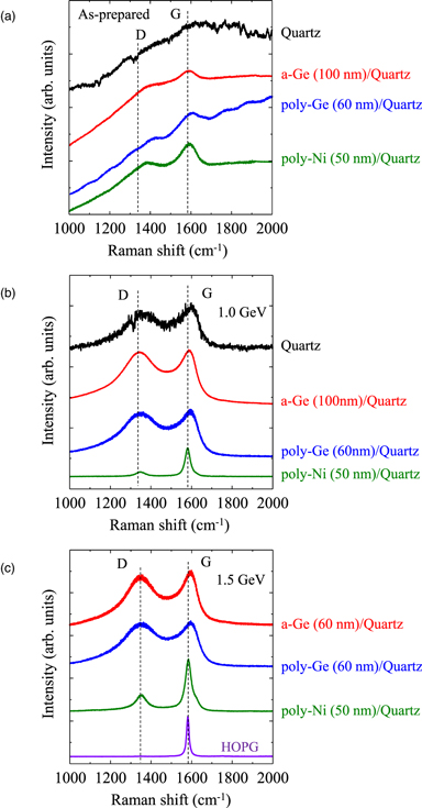
Fig. 2. (Color online) Raman spectra of (a) as-prepared and ((b) and (c)) soft X-ray irradiated HMD C films on quartz, a-Ge, poly-Ge, and poly-Ni. The eye-guide lines of D band (defect in graphene) at 1350 cm−1 and G band (graphene) at 1575 cm−1 are shown. Storage-ring energies were 1.0 (b) and 1.5 GeV (c). Raman spectrum of HOPG is also shown in (c) as a reference.
Download figure:
Standard image High-resolution image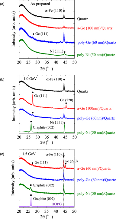
Fig. 3. (Color online) XRD patterns of (a) as-prepared and ((b) and (c)) soft X-ray irradiated HMD C films on quartz, a-Ge, poly-Ge, and poly-Ni. Diffraction peaks owing to graphite, Ge, and Ni are denoted by closed square, closed circle, and open circle, respectively. The arrows indicate the diffraction peak from the sample stage of α-Fe (110). XRD pattern of HOPG is also shown in (c) as a reference.
Download figure:
Standard image High-resolution imageFollowing soft X-ray irradiation, the crystallinities of the Si and Ge films, poly-Ge, and poly-Ni underlayers were improved owing to enhanced atom movement via electron excitation. 22) The intensity of Ge diffraction peaks after soft X-ray irradiation was larger for poly-Ge film generated from a-Ge film/quartz than that generated from poly-Ge film/quartz as shown in Fig. 3(b). The reason is not clear, but it may be due to the enhancement of the a-Ge crystallization during soft X-ray irradiation by the carbon film. 23) In addition, the Ge diffraction peak of the poly-Ge film obtained from poly-Ge film/quartz at 1.5 GeV was not observed in Fig. 3(c) due to a decrease in diffraction signal by the partial exfoliation of the sample under the high storage-ring energy condition of 1.5 GeV. In addition, a broad peak, which corresponds to amorphous C or small clusters of graphite, was observed on the Raman spectra of the C films on the quartz substrate, a-Ge and poly-Ge film/quartz substrates. In contrast, sharp G (1581 cm−1), D (1344 cm−1), and 2D (2694 cm−1) peaks were observed for the Ni film/quartz substrate sample. However, its FWHM value is larger than that of the highly-oriented pyrolytic graphite (HOPG). The XRD peak due to graphite (002) was only observed in the diffraction pattern of the C film on the Ni underlayer after soft X-ray irradiation. The FWHMs of the C film on the Ni underlayer and HOPG were 0.48° and 0.21°, respectively. The FWHM of the diffraction peak is related to the crystal grain size. The results imply that nanographene could be synthesized only from the C film on the Ni underlayer by soft X-ray irradiation.
3.2. Influence of photon energy on the properties of nanographene on the Ni underlayer
The peak position, FWHM, and intensity ratio of the D to G peak (ID/IG) in the Raman spectra of the nanographene prepared at various photon energies are shown in Fig. 4. The positions of the D, G, and 2D peaks exhibited an upward shift with increasing photon energy. The peak position was related to strain. 24) Therefore, the compressive stress on the nanographene increased with increasing photon energy. The FWHM of the D peak reached a maximum value of 108 cm−1 at 200 eV and then decreased. The D peak is related to the defects in the graphene flakes. Thus, the graphene obtained at 200 eV exhibited many defects or small grains. The quality of graphene is often determined by the formation temperature. 25,26) The sample temperature at 200 eV was 760 °C and was the lowest under all soft X-ray irradiation conditions. However, at 300 eV, the FWHM of the D peak had the lowest value (63 cm−1), despite the temperature (780 °C) being almost the same as that at 200 eV. In addition, the ID/IG ratio had the highest value of 0.4 at 150 eV. Thus, the quality of nanographene is determined not only by the formation temperature, but also by the effect of soft X-rays.
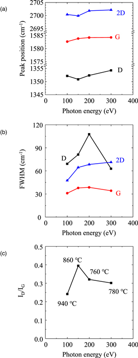
Fig. 4. (Color online) (a) Peak position, (b) FWHM, and (c) ID/IG in the Raman spectra of C films prepared on poly-Ni/quartz substrate at various photon energies.
Download figure:
Standard image High-resolution imageThe effects of photon energy and sample temperature on the peak positions and FWHM values obtained from the XRD patterns are shown in Fig. 5. The peak positions shifted upwards, and the FWHM increased by increasing the photon energy to 150 eV. Both parameters were saturated in the range of 150–300 eV. With the change in the photon energy, the trends observed for the changes in the peak positions and FWHM values were similar. Based on these results the quality of nanographene was found to depend, not only on the formation temperature, but also on the effects of soft X-ray irradiation. This corresponds well to the previous observation from the results of the Raman scattering experiments.
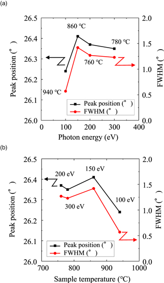
Fig. 5. (Color online) Effect of (a) photon energy and (b) sample temperature on the peak position and FWHM values in XRD patterns of HMD carbon/poly-Ni/quartz substrate after soft X-ray irradiation.
Download figure:
Standard image High-resolution image3.3. Synthesis mechanism of nanographene on Ni underlayer by soft X-ray irradiation
The formation mechanism of nanographene was studied considering the comparative effect of the photon energy on the Ni and Ge underlayers. The calculated absorption curves of soft X-rays for C, Ge, and Ni are shown in Fig. 6. 27) The amount of the X-ray absorbed at 300 eV by the Ge and Ni underlayers was greater than that by the C film. With the decrease in photon energy, the amount of the X-ray absorbed by the Ge and Ni underlayers increased. Conversely, the X-ray absorbed by C decreased to 280 eV, but increased above 285 eV owing to electron excitation from the C 1s orbital level at 284.6 eV.

Fig. 6. (Color online) Calculated absorption of C, Ni, and Ge as a function of photon energy. 27) The photon energies of the irradiated soft X-ray are shown as arrows.
Download figure:
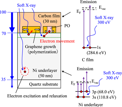
Standard image High-resolution imageFrom the estimation of the soft X-ray absorption, the polymerization mechanism considering the effects of the underlayer is presented in Fig. 7. The soft X-rays were directly absorbed by the HMD C film. The occurrence of electron excitation from the C 1s orbital level promoted the chemical reactions, such as the C–H bond breaking and the C=C bond formation. However, major C=C bond formation did not occur because nanographene was not generated from the HMD C film containing the Pn-based precursor and PO on the quartz substrate, as shown in Fig. 2(b). The C film with a thickness of 30 nm absorbed 30% of the soft X-rays at 300 eV, and the transmitted soft X-rays penetrated the Ge or Ni underlayer. The Ge and Ni atoms at the underlayer absorbed the soft X-rays, which excited the electrons in the electron orbitals. Thereafter, the electrons at the interface between the C and the metal underlayer films moved into the C film. Certain chemical reactions, such as C–H bond breaking and C=C bond formation, were enhanced by the photoelectron transfer reaction 28) owing to the soft X-ray excitation and to excitation of the electrons from the underlayer film. The difference in graphene quality, as revealed by the FWHM of the D peak and ID/IG ratio, can be explained by comparing the effects of the photon energy on the characteristics of the Raman spectra and the soft X-ray absorption. The change in the FWHM of the D peak [Fig. 4(b)] is related to the absorption by the C film. The supply of electrons from the Ni underlayer is considered necessary to grow nanographene, and the excited electrons in the C film promote defect removal and/or nanographene growth. From 100 to 200 eV, the ID/IG ratio was the lowest at 100 eV because the absorption by the C film and Ni underlayer was at maximum. The ID/IG ratio is related to the balance between the absorption by the C and Ni underlayers.
Fig. 7. (Color online) Illustration of the effect of soft X-rays on the polymerization reaction of HMD C film on Ni underlayer. The values on the left-hand side denote the photon number of X-ray at 300 eV scaled to a maximum value of 100. The core levels of C and Ni are shown on the right-hand side. The region where the electrons are supplied to the carbon film is indicated by the dotted, green-line.
Download figure:
Standard image High-resolution image
Electron excitation by soft X-ray absorption in the C film may have contributed to the formation of graphene. 18) If so, graphene would have been formed both on the Ge and the Ni underlayer. However, the effect of the excited electrons was negligible because graphene was not formed on the Ge underlayer. The possible reasons for the formation of graphene on the Ni underlayer are discussed in detail in the next section.
3.4. Difference in catalytic activity between the Ge and Ni underlayers during soft X-ray irradiation
In this section, the difference between the effects of Ge and Ni underlayers on nanographene synthesis during soft X-ray irradiation is discussed. The amount of X-ray absorption at 300 eV for the Ge underlayer was higher than that for the Ni underlayer. When the thicknesses of the Ge and Ni underlayers were almost the same, the amount of absorption was approximately the same, as shown in Fig. 6. The excited electrons from the ∼3 nm surface of the Ge and Ni films are supplied to the C film. At such conditions, the absorption of the Ge and Ni films was estimated to be 4% and 5%, respectively. Considering the absorption, there was no difference between the properties of the Ge and the Ni films. 27) However, nanographene was synthesized only on the Ni underlayer under the present conditions. Therefore, the difference between Ge and Ni cannot be explained by the amount of X-ray absorption.
A possible reason for this is the difference in the solubility of C. The mechanism of graphene synthesis in thermal CVD has been investigated based on the solubility of C in metals and surface reactions. 2) In addition, the crystal orientation and grain size of the metal are strongly related to the properties of graphene. 29) The solubility of C in Ni was estimated to be 0.9 at% at 900 °C, 30) 2.0 at% at 1000 °C, 31) and 2.9 at% at 1326 °C. 32) For the CVD growth on Ni, the nanographene grew via surface catalytic growth, including the dissolution of C. In contrast, the solubility of C in Ge was estimated to be <0.1 at%. 33) It was also regarded as a self-limiting and surface-mediated process similar to the Cu-catalyzed growth of graphene because of the low solubility of C in Ge. 21) Graphene synthesis was not successful on Ge, but this may be due to the difference in the mechanisms of graphene growth. However, graphene synthesis via a combined HMD and soft X-ray irradiation is different from CVD growth on Ni. During soft X-ray irradiation for the growth of HMD C films, the benzene structure of the Pn molecule was maintained. Therefore, nanographene was generated by a surface-mediated process, despite its growth on the Ni surface. Hence, the difference in the CVD growth mechanisms owing to the solubility of C does not explain the absence of graphene growth on the Ge underlayer.
Another reason could be the difference in the ease of graphene synthesis on the Ge and Ni films, that is, the difference in catalytic activity between the Ge and Ni underlayers during the soft X-ray irradiation. In graphene growth using CVD, the critical growth temperature on the Ge substrate (910 °C 21)) is higher than that on the Ni substrate (550 °C 30)). It has been reported that the activation energy of graphene growth on Ge is 7.2 eV, 34) which is higher than that of Cu (3 eV). 35) The difference between the catalytic activity of the Ge and Ni underlayers was attributed to the difference in the critical temperatures for graphene formation. To understand the influence of growth temperature on graphene synthesis, soft X-rays were also irradiated onto the HMD C films on a-Ge and poly-Ge underlayers at a high storage-ring energy of 1.5 GeV. The sample temperature was as high as 1000 °C under such irradiation conditions. Despite exceeding the growth potential temperature on the Ge substrate during the CVD process, graphene was not produced, as shown in Figs. 2(c) and 3(c). In this experiment, we attempted to synthesize graphene using a post-treatment (soft X-ray irradiation), instead of a direct growth (CVD). Therefore, the growth mechanism and the growth temperature are expected to be different in CVD and soft X-ray irradiation.
The catalyst reduces the activation energy for breaking the C–H bond in the CVD of graphene. Therefore, a low temperature of approximately 1000 °C, in comparison to a growth temperature of approximately 1400 °C in a metal-free CVD, was realized to synthesize graphene using a metal catalyst. 36,37) In the case of Ni, the CVD growth of graphene occurred via a C segregation or precipitation process. 30) In addition, metal-catalyzed crystallization of amorphous C to graphene via layer exchange through thermal annealing has been demonstrated. 38,39) Furthermore, in plasma CVD, graphene was produced using neutral and ionized hydrocarbon precursors. 40) Therefore, plasma-enhanced CVD shows considerable potential for low-temperature graphene growth, as well as direct graphene growth on dielectric substrates without a metal catalyst. 41)
Conversely, immiscible Ge–C systems under equilibrium conditions have been reported to direct graphene growth on Ge via a self-limiting and surface-mediated process rather than a precipitation process. This observation corresponds well to reports that employed other metals, namely, Ni, Ru, Ir, and Pt, with high solubility of C. 21) Furthermore, similarities between the C−Ge and C−Cu material systems, namely, in the comparable catalytic activity, the extremely low solubility of C, and absence of a stable carbide, have also been reported. 19) It is reported that near the melting point of Ge, its catalytic activity toward the hydrogenation of C is sufficient to enable the growth of high-quality graphene. 42)
Thus, the CVD growth mechanisms of graphene on Ge and Ni surfaces have been reported. However, the difference in the catalytic activities remains unclear, and in particular, the behavior of the electrons has not been investigated. The catalytic effects on the chemical reactions are related to the electrons in the d orbital. The d electrons are highly localized. As such, selective binding is likely to occur. The open-shell nature of the d electrons of Ni is known to affect the activation of dehydrogenation. 43) Conversely, Ge consists of closed-shell d electrons. Therefore, the catalytic effects on the chemical reactions of Ge are likely to be weaker than those of Ni. The Ge d electrons become open shells via the Auger process owing to the electron excitation by soft X-ray irradiation. However, this process is inadequate for reducing the growth temperature of nanographene on the Ge underlayer, which is an important condition for graphene synthesis. However, under low-temperature conditions below the synthesis temperature of graphene, the effect of soft X-ray irradiation was more pronounced in the case of the Ni underlayer, which may be due to the effect of excited electrons. Furthermore, the unsuccessful nanographene synthesis on the Ge underlayer might include poor crystallinity and the influence of the natural oxide film on the Ge surface. Therefore, the effects of soft X-rays on catalytic enhancement need to be investigated further.
4. Conclusions
Sharp Raman peaks corresponding to the G and D bands were obtained at 760 °C only for the Ni underlayer. Conversely, in both the a-Ge and poly-Ge underlayers, broad peaks attributed to amorphous C or graphite with small grain sizes were obtained despite the high-temperature treatment at approximately 1000 °C during soft X-ray irradiation. The Ni underlayer enhanced the polymerization by catalytic activation, in addition to electron excitation during soft X-ray irradiation. Results showed that the differences between the properties of the Ge and Ni underlayers lead to the observed difference in their catalytic activities.
Acknowledgments
This study was partially supported by JSPS KAKENHI (Grant No. 15K04611). The authors would like to acknowledge Dr. Izumi of the Hyogo Prefectural Institute of Technology for his help with XRD measurements.