
Abstract
Atomic diffusion bonding with oxide underlayers using Al and a-Si films was examined to create a bonded interface with Al2O3 and Si-oxides having large band gaps for high optical density applications. Surface free energy of the bonded interface greater than 2 J m−2 and 100% light transmittance were achieved after annealing at 300 °C in the range of film thicknesses δ on both sides from 0.3 to 0.5 nm using Al films and with δ of around 0.5 nm using a-Si films. Structural analyses revealed that the bonded interface consists of Al2O3 and Si-oxides with oxygen dissociated from oxide underlayers.
Export citation and abstract BibTeX RIS
1. Introduction
As the output power of laser devices increases, highly reliable optical elements have become increasingly necessary for laser optics. For example, polarizing beam splitters that consist of two optical glasses bonded together are representative optical elements used in high-brightness projectors. 1,2) Actually, bonding is performed between the optical thin films deposited on the bonding surfaces of two optical glasses. In conventionally used polarizing beam splitters, the glass surfaces coated with optical films are bonded using organic adhesives such as epoxy and polyimide. Intense beams of photons and thermal energy emitted from lasers degrade the organic adhesive layer. Moreover, the bonding strength degradation of organic adhesives which occurs over time because of humidity and water ingress also presents difficulties. 3)
Furthermore, in optics for lasers, laser beams with a short wavelength or short pulse width are known to destroy optical thin films because of photon absorption and thermal diffusion. Especially for optical application for UV-wavelength continuous-wave laser beams or femtosecond pulsed lasers, optical thin films consisting of a larger bandgap are used. 4–6) That is true because a larger bandgap has a higher laser-induced damage threshold (LIDT). 4,5) It is therefore necessary that the bonded interface be formed with materials having an LIDT that is as large as possible.
Consequently, a new bonding method with high light transmittance, strong bonding energy sufficient to withstand the post-cutting process, and high durability against higher energy photons are required for a light-transmitting interface of high optical density devices. Moreover, the bonding technique must be applicable to amorphous materials such as glass substrates and dielectric multilayers with bonding temperatures lower than the glass transition temperature (Tg).
Atomic diffusion bonding (ADB) of two flat substrates using thin metal films is a promising process to achieve bonding at room temperature, 7–11) along with surface-activated bonding. 12–18) In ADB processing, bonding can be done even with film thickness of a few angstroms on each side. In bonded transparent wafers such as quartz crystal or amorphous glass, the incident light can be transmitted through thin bonded films with no marked reduction in intensity. The use of thin Ti films is effective for achieving both high optical transmittance and high bonding strength. However, optical energy absorption of 2% remains at the bonded interface even when the wafers are bonded using 0.2 nm thick Ti film on each side. Reduction of the Ti film thickness below 0.2 nm further enhances the transmittance, but it reduces the bonding strength considerably. 9)
To overcome this difficulty, we proposed ADB using oxide underlayers. 19) Figure 1 portrays a schematic illustration of this method. For this method, oxide underlayers are deposited on two wafer's surfaces, then the wafers are bonded using ADB with thin metal films in vacuum at room temperature as a usual atomic diffusion process. Thereafter, the bonded sample is annealed in air at 150 °C–300 °C, which is sufficiently lower than Tg. This annealing enhances the oxidation of thin metal films with oxygen dissociated from oxide underlayers. Then high light transmittance can be achieved along with high bonding strength. Actually, quartz glass wafers with a SiO2 underlayer deposited using ion-beam-assisted deposition (IAD) were bonded with a thin Ti film. Results indicate that, even with a 1 nm thick Ti film on each side for bonding, the bonded interface changed to TiO2 or Ti4O7-like Ti oxide after post-bonded annealing at 300 °C. 20) In fact, 100% light transmittance and surface free energy of the bonded interface of more than 2 J m−2 were achieved. 19–21) Herein, 100% light transmittance indicates that the loss of optical power at the bonded interface is less than the detection limit. The IAD method, a widely used technique for formulating optical thin films, 22) can be used for bonding interfaces with optical thin films such as dielectric multilayers.

Fig. 1. (Color online) Schematic illustration of atomic diffusion bonding with oxide underlayers and post-bonded annealing.
Download figure:
Standard image High-resolution imageAlthough ADB using oxide underlayers is useful, higher optical density applications require that the bonded interface be formed with materials having larger LIDT than those of Ti oxides. Table I presents the crystal structures of Ti, Zr, Hf, Al, and amorphous Si (a-Si), oxide compounds from these elements, in addition to values of free energies of formation of the oxide compounds from the elements at 300 K, ΔG. 23) The table also presents values of the optical bandgap Eg 5) and the refractive index nd 24–28) of these oxide compounds. Here, the nd values were measured using the Fraunhofer helium d spectral line at wavelength λ of 587.6 nm, which is commonly used for lens materials.
Table I. Crystal structure of Ti, Zr, Hf, Al, and amorphous Si (a-Si), oxide compounds from these elements, with values of free energies of formation of the oxide compounds from the elements at 300 K, ΔG. Values of optical bandgap Eg and refractive index (at λ = 587.6 nm) nd of these oxide compounds are also presented.
| Film materials | Crystal structure | Oxide compounds from the elements and their properties | |||
|---|---|---|---|---|---|
| Oxide compounds | Free energies of formation of oxide compounds from the elements at 300 K, ΔG (kJ mol−1 of compounds) | Optical film bandgap, Eg (eV) | Refractive index, nd (λ = 587.6 nm) | ||
| Ti | Hcp | TiO2 | −862 | 3.6 | 2.61 24) |
| Zr | Hcp | ZrO2 | −1042 | 4.74 | 2.15 25) |
| Hf | Hcp | HfO2 | −1053 | 5.2–5.3 | 1.89 26) |
| Al | Fcc | Al2O3 | −1584 | 6.46 | 1.67 27) |
| a-Si | Amorphous | SiO2 | — | 7.49 | 1.46 28) |
Actually, Zr and Hf have hcp structures resembling that of Ti. Moreover, the absolute values of ΔG for Zr and Hf are nearly identical to that for Ti. Therefore, it is reasonable to infer that these material films (the films of these transition metals) are useful for ADB using oxide underlayers similarly to Ti films. We applied Hf films for ADB using oxide underlayers. The light transmittance reached 100% at an annealing temperature of 300 °C, with great bonding strength, even with a 1 nm thick Hf film on each side for bonding. 29) The performance achieved using Hf films is nearly identical to that using Ti films, although the bonded interface structure using Hf films remained under examination. The important difference is that the values of Eg of ZrO2 and HfO2 are, respectively, 4.74 eV and 5.2–5.3 eV, as shown in Table I, which are remarkably larger values than that of TiO2 (Eg = 3.6 eV). The nd values of HfO2 and ZrO2 are smaller than that of TiO2 because the values of Eg and refractive index share a tradeoff relation. 5) Therefore, Zr and Hf are more promising film materials than Ti when used for ADB with oxide underlayers for higher optical density applications.
From the viewpoints of higher LIDT, the Eg values of Al2O3 (6.46 eV) and SiO2 (7.49 eV) are much greater than others, although nd values of these materials are even lower than those of the others. We have reported that ADB can be conducted using a-Si films, although Si is a representative semiconductor material and not metal. 8) Therefore, it would be very useful if thin Al and a-Si films could be used for ADB with oxide underlayers, as is true using Hf and Ti films: we can expect the formation of a highly durable bonded interface against higher energy photons generated by laser beams with a short wavelength or short pulse width and high peak intensities. The absolute value of ΔG for Al is larger than that of Hf or Ti, indicating the potential for oxide formation at low temperatures using Al films, although we have no data indicating ΔG of a-Si. An important point of concern is that Al2O3 and SiO2 are materials with a strong covalent bond. Therefore, it is not clear that these materials films are as useful as Hf and Ti films: at least the bonding condition to achieve high light transmittance and bonding strength at a low annealing temperature are expected to be unlike those using Hf or Ti films.
For this study, we applied Al and a-Si films for ADB using oxide underlayers. Structural and optical properties of the bonded interface were examined as functions of film thickness and annealing temperature by comparison to those using Zr or Hf film. For the oxide underlayers and substrate, the SiO2 underlayer and quartz substrates were used as described in our earlier reports to examine materials used for bonding films. We discussed the potential of ADB using oxide underlayers to form the bonded interface with materials having larger LIDT for higher optical density applications.
2. Experiment methods
Synthetic quartz glass wafers with 0.5 mm (or 0.7 mm) thickness and 2 inch diameter were used for the substrate. Using the IAD method, a 5000 nm SiO2 underlayer was deposited. Then the SiO2 underlayer surface was polished carefully using chemical mechanical polishing. Surface roughness Sa was evaluated as 0.3 nm or less using atomic force microscopy. Wafers with a SiO2 underlayer were introduced into a vacuum chamber with a base pressure of less than 5 × 10⁻⁷ Pa. Thin films were sputter-deposited on two flat oxide underlayer surfaces. Then, the bonding of the two films on the wafers was conducted under vacuum at room temperature. The film thickness was controlled by the sputter-deposition time under a constant low deposition rate in each material film. In the post-bonded annealing processes, the bonded wafers were extracted from the vacuum chamber into the atmosphere and were subsequently heated in air using an oven. The annealing temperature varied from 50 °C to 400 °C by 50 °C, but the annealing time was fixed at 4 h.
The total transmittance (T) and total reflectance of the substrate (R) were measured using a spectrophotometer (UH-4150; Hitachi High-Technologies Corp.). Then, the internal transmittance of the bonded interface (Tin), considering multiple reflections of the substrate and multiple absorptions of thin bonded films, was calculated using Eqs. (1) and (2). 30)

In those equations, R0 denotes the surface reflectance of the substrate. Optical measurement procedures are shown in Fig. 2. The probe light enters the substrate almost perpendicularly.
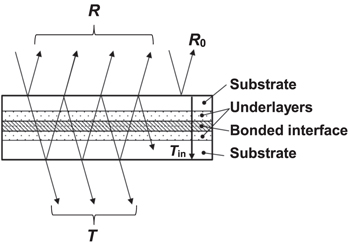
Fig. 2. Optical measurement procedure for samples considering multiple reflections and multiple absorptions of thin bonded films. R0 is the surface reflectance of the substrate.
Download figure:
Standard image High-resolution imageThe surface free energy of the bonded interface γ was evaluated using the blade method reported by Maszara. 31) The value of γ was found for wafers as-bonded and after post-bonding annealing at 300 °C.
3. Results and discussion
3.1. Light transmittance and γ values
Figures 3(A) and 3(B) present the internal transmittance (Tin) of a bonded interface using Al and a-Si films as a function of post-bonded annealing temperature. Here, the averaged values of transmittance of visible light from 400 to 700 nm are shown. Five series of data with films of various thicknesses on one side δ of 0.2, 0.3, 0.4, 0.5, and 1.0 nm used for bonding are shown for each figure. Figures 3(C) and 3(D) present results obtained for bonded interfaces of Zr and Hf film for comparison.

Fig. 3. (Color online) Values of the internal transmittance of the bonded interface using (A) Al and (B) a-Si films as a function of post-bonded annealing temperature. Here, averaged values of transmittance of visible light from 400 to 700 nm are shown. Results obtained for a bonded interface using Zr or Hf film are shown for comparison in (C) and (D).
Download figure:
Standard image High-resolution imageRegarding the Al films shown in panel (A), the transmittance of all wafers increased remarkably as the annealing temperature increased beyond 200 °C. This result is similar to those obtained using Hf and Zr, as shown in panels (C) and (D). Using Al films, the light transmittance of 100% was achieved at annealing temperatures of 300 °C for interfaces bonded with δ = 0.5 nm or less. This finding differs from that obtained using Hf and Zr films: light transmittance of 100% was achieved even with δ of 1.0 nm at the annealing temperature of 300 °C. Using Al films of δ = 1.0 nm, the annealing temperature had to be increased beyond 400 °C to achieve 100% light transmittance.
It is noteworthy that the values of light transmittance using a-Si films with δ = 0.5 nm or less, as shown in panel (B), were greater than those achieved using other film materials because light transmittance through pure Si in the visible light region is higher than that of the others. These transmittances increase gradually as the annealing temperature increased and achieved 100% at 300 °C, as when other material films were used. However, similarly to results obtained using Al film, when using a-Si films with δ of 1.0 nm, 100% light transmittance was unobtainable, even at an annealing temperature of 400 °C. These results indicate that 100% can be achieved using Al and a-Si films, as even using Hf and Zr, although the film thicknesses used for bonding are limited to those of less than 0.5 nm.
Figures 4(A)–4(D) present the values of surface free energy at the bonded interface γ of these samples as a function of δ. Data for as-bonded samples and those after annealing at 300 °C are shown. In addition, γ for as-bonded samples increased concomitantly with increasing δ in all series of samples. Moreover, annealing at 300 °C enhanced the γ values considerably.
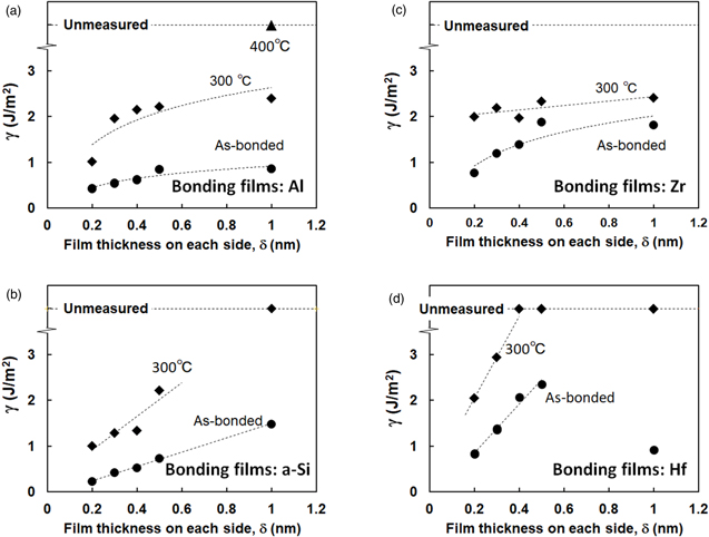
Fig. 4. (Color online) Values of the surface free energy at the bonded interface γ using (A) Al, (B) a-Si, (C) Zr, and (D) Hf films as a function of post-bonded annealing temperature.
Download figure:
Standard image High-resolution imageUsing Al and a-Si films, γ reached high values greater than 2 J m−2 after annealing at 300 °C in the δ range greater than 0.3 nm with Al films and greater than 0.5 nm with a-Si films. This finding differs from those obtained when using Zr and Hf films: γ reached high values greater than 2 J m−2 after annealing at 300 °C in the wide δ range greater than 0.2 nm. Particularly, γ is remarkably high using Hf films thicker than 0.4 nm: a blade could not be inserted between the bonded wafers.
Results indicate that high γ values greater than 2 J m−2 and 100% light transmittance can be achieved also using Al and a-Si films after annealing at 300 °C. However, this achievement was limited in the δ range of 0.3–0.5 nm using Al films and with δ of around 0.5 nm using a-Si films. These δ ranges are narrower than those obtained using Zr or Hf film: high γ values greater than 2 J m−2 and 100% light transmittance can be achieved for δ ranges of 0.2–1 nm.
3.2. Interface structure
First, a bonded interface structure obtained using Hf films is discussed to assess the occurrence of oxidation of Hf films, which is similar to that of Ti films. Figure 5(A) portrays a cross-section image of the bonded interface obtained using Hf films with δ = 1 nm after annealing at 400 °C, as observed using transmission electron microscopy (TEM). The light transmittance of the bonded interface of these samples reached 100% at annealing temperatures higher than 300 °C, as shown in Fig. 3. Panel (B) presents an annular dark field (ADF) image of this sample evaluated using a scanning transmission electron microscope (STEM). Panels (C-1)–(C-3) portray mapping images of Hf, O, and Si obtained from electron energy loss spectroscopy (EELS) analysis 32) of the region shown by the dotted line in (B). These images were obtained from the Hf–M, O–K, and Si–L edges of the EELS spectra. The EELS spectra near the Hf–M and Si–L edges obtained along lines a–e shown in (B) are presented in panel (D). The bonded interface structure shown in panel (A) was amorphous. The bonded interface thickness was 4.4 nm. This thickness is more than twice that of the original total thickness of Hf films (2 nm). No marked diffusion between Hf and Si is apparent in panels (C-1) and (C-3). However, no clear boundary between bonded interface layer and SiO2 underlayers was found from O mapping (C-2), which indicates that the oxygen dissociated from the SiO2 underlayer diffuses into the Hf film. Furthermore, the spectrum along line c, the center of the thickness, in panel (D) shows good agreement with the spectrum of HfO2, 33) indicating that HfO2 is formed as the interface layer. The Si-K edge is also observed in the spectrum, but this is attributable to the fact that the spatial resolution of the EELS analysis is approximately equal to the interface layer thickness. Actually, the spectra of SiO2 underlayers, observed along with lines a and e, overlap those along lines b–d. It is noteworthy that those spectra around the Hf–M edge examined along with lines b and d are almost identical to that with line c, suggesting the homogeneous formation of HfO2 in the interface layer. These results indicate that the HfO2 layer is formed by oxygen dissociated from the SiO2 underlayer by annealing after bonding, which is true also when using Ti films. 20)
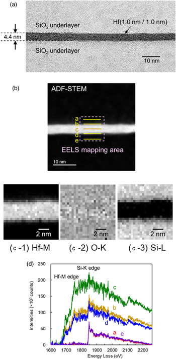
Fig. 5. (Color online) (A) a TEM cross-section image of the bonded interface using Hf films with δ = 1 nm after annealing at 400 °C, (B) ADF-STEM image of the bonded interface, EELS mapping of (C-1) Hf, (C-2) O, and (C-3) Si observed in the mapping area shown in (B), and (D) EELS spectra around Hf–M edge and Si-K edge obtained for scanning lines of a–e in (B).
Download figure:
Standard image High-resolution imageUsing Al films, the light transmittance of 100% was achieved at annealing temperatures of 300 °C for interfaces bonded with δ less than 0.5 nm. Figure 6 portrays STEM cross-section images of bonded interfaces using Al films with δ = 0.5 nm after annealing at 400 °C: (A) a bright field (BF) image and (B) a high-angle annular dark field (HAADF) image. No interface corresponding to the original film surfaces was observed. The interface layer was amorphous and two-dimensionally homogeneous. The interface layer thickness estimated from the images was 2.0 nm: almost twice the total thickness of the original Al films. This finding is identical to those obtained for the Hf film shown in Fig. 5(A).
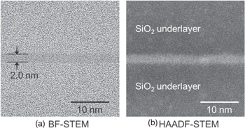
Fig. 6. STEM cross-section images of the bonded interface using Al films with δ = 0.5 nm after annealing at 400 °C: (A) bright field image and (B) high-angle annular dark field image.
Download figure:
Standard image High-resolution imageFigure 7(A) presents an ADF-STEM image of the bonded interface for the same sample shown in Fig. 6. Mapping images of Al, Si, and oxygen atoms in the dashed-box examined using EELS are presented in panels (B)–(D). No significant diffusion was observed between Al and Si layers. Oxygen was observed in the bonded interface layer of Al films, which was likely to be dissociated from SiO2 underlayers.
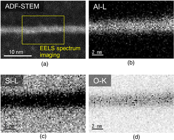
Fig. 7. (Color online) (A) An annular dark field scanning transmission electron microscopy image of the bonded interface for the same sample shown in Fig. 6. EELS Mapping of Al, Si, and oxygen atoms in the dashed-box area in panel (A) is shown in panels (B)–(D).
Download figure:
Standard image High-resolution imageFigure 8 presents the EELS spectra of this sample. Spectra were analyzed in the bonded interface layer and in the SiO2 underlayer. A spectrum for Al2O3 34) is also shown for comparison. The spectrum in the interface layer, which is almost identical to that of Al2O3, is overlapped by that of in SiO2 underlayer in the range of energy loss greater than 100 eV. This apparent overlapping is attributable to the fact that the spatial resolution of the EELS analysis is approximately equal to the interface layer thickness.
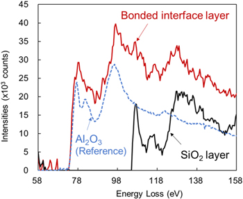
Fig. 8. (Color online) EELS spectra of the sample portrayed in Fig. 7. Spectra analyzed in the bonded interface layer and in the SiO2 underlayer are shown. A spectrum for Al2O3 is also depicted for comparison.
Download figure:
Standard image High-resolution imageThese results revealed that Al films used for bonding, with δ = 0.5 nm, were oxidized by annealing. Moreover, the interface layer consists of amorphous Al2O3. These structural analyses were conducted for the sample annealed at 400 °C, but it is reasonable to infer that Al2O3 formation occurred at 300 °C: light transmittance reached 100% at the annealing temperature of 300 °C, as shown in Fig. 3.
We examined the values of bonded interface thicknesses quantitatively. Figure 9 presents the thicknesses and characteristics of interfaces bonded using Al (δ = 0.5 nm), Hf (δ = 1 nm), and Zr (δ = 1 nm) films as a function of calculated thicknesses of oxide films. The data for Al (δ = 0.5 nm) and Hf (δ = 1 nm) films were evaluated from the TEM images presented in Figs. 5(A) and 6. The interface thickness for Zr (δ = 1 nm) was evaluated from TEM images observed for the bonded interface obtained using Zr films with δ = 1 nm after annealing at 400 °C, similarly to those obtained using Al and Hf films, although those images are not presented herein. Assuming that these metal films form oxide compounds with oxygen dissociated from SiO2 underlayers, we calculated the thickness of the formed oxide layers of Al2O3, HfO2, and ZrO2. The molar densities of crystalline oxides were used for calculation. In the figure, results obtained using Ti (δ = 1 nm) 20) and Nb (δ = 1 nm) films are also shown as a function of the calculated thickness of oxide films assuming the formation of TiO2 and Nb2O5.

Fig. 9. Values of interface thicknesses bonded using Al (δ = 0.5 nm), Hf (δ = 1 nm), and Zr (δ = 1 nm) films evaluated from TEM images as a function of the calculated thickness of oxide films assuming the formation of Al2O3, HfO2, and ZrO2. In the figure, results obtained using Ti (δ = 1 nm) and Nb (δ = 1 nm) films are also shown as a function of the calculated thickness of oxide films assuming the formation of TiO2 and Nb2O5.
Download figure:
Standard image High-resolution imageThe light transmittance of the bonded interface using these films also achieved 100% at an annealing temperature higher than 300 °C, although data obtained using Nb films are not presented herein. The values of the bonded interface thicknesses show good agreement with those of calculated oxide layers, although the values of bonded interfaces are slightly larger than the calculated values. Moreover, the bonded interface thickness presents a good linear relation with that of the calculated oxide layer. This finding supports the formation of these oxide materials at the bonded interface using these films, yielding 100% optical transmittance of the bonded interface.
It is noteworthy that the interface bonded using Al films with δ = 1 nm is remarkably different from those described above. Figure 10 portrays TEM cross-section images of the bonded interface using Al films with δ = 1 nm, obtained after annealing at 400 °C. When using Al films of δ = 1.0 nm, the annealing temperature had to be increased beyond 400 °C to obtain 100% light transmittance, as shown in Fig. 3(A). The bonded interface, which comprises fine grains, is remarkably unlike the two-dimensionally homogeneous interface obtained using Al films with δ = 0.5 nm shown in Fig. 6. One can reasonably infer that Al films with δ = 1.0 nm deposited on the SiO2 underlayer show an island-like structure and that the bonded interface is discontinuous. Moreover, Al2O3 is extremely stable because of the covalent bonding between Al and oxygen. Therefore, it is likely that oxidation proceeds from the grain boundaries of the bonded Al layer. It is also likely that Al2O3 formed on grain surfaces prevents the progress of oxidation into the grain interior.
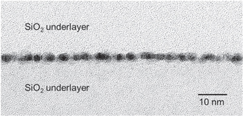
Fig. 10. TEM cross-section images of the bonded interface using Al films with δ = 1 nm after annealing at 400 °C.
Download figure:
Standard image High-resolution imageThe bonded interface structure which exists when using a-Si films is remarkably different from that observed when using Al films. Figure 11(A) shows a cross-section TEM image of the bonded interface using a-Si thin films with δ = 1 nm thickness after annealing at 400 °C. Using a-Si films with δ = 1 nm, 100% light transmittance was not achievable, even with an annealing temperature of 400 °C, as shown in Fig. 3(B). A slightly dark broad line corresponding to the bonded interface was observed in the image, indicating that a-Si films used for bonding has been oxidized perfectly with oxygen dissociated from oxide underlayers. The boundary between the bonded interface and the SiO2 underlayer is unclear, which is also a point of difference from those of interfaces using other material films. It is noteworthy that lattice images are partially observed, suggesting that the light and shade portrayed in the image represent diffraction contrast. Panels (B-a) and (B-b) show FFT patterns obtained from areas (a) and (b) in panel (A). The FFT patterns support our inference that the bonded interface was partially crystalline. Surprisingly, the spot distance in FFT patterns suggests the formation of crystalline Si from a-Si films, although we were unable to obtain clear evidence of that formation. Oxidation of the a-Si layer proceeds from the interfaces with the SiO2 underlayer, but Si-oxides are very stable, as is Al2O3. Therefore, it is likely that Si oxides formed on the surfaces of bonded a-Si layers prevented the progress of oxidation into the interior of the a-Si layer, similarly to results obtained using Al films.

Fig. 11. (Color online) (A) TEM image of the bonded interface using a-Si thin films with δ = 1 nm thickness after annealing at 400 °C. (B-a) and (B-b) FFT pattern obtained from areas (a) and (b) in the image (A).
Download figure:
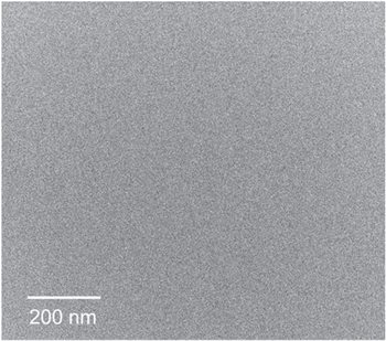
Standard image High-resolution imageWe also conducted TEM analyses for the bonded interface using a-Si thin films with δ = 0.5 nm thickness after annealing at 400 °C, where 100% light transmittance can be achieved. Nevertheless, we were unable to find any contrast corresponding to the bonded interface, as presented in Fig. 12. This result is well-consistent with and indicative of the homogeneous formation of Si oxide at the bonded interface.
Fig. 12. TEM image of an area in which the bonded interface exists. Bonding was performed using a-Si thin films with δ = 0.5 nm thickness, with annealing at 400 °C.
Download figure:
Standard image High-resolution image
4. Conclusions
By applying Al and a-Si films for ADB using oxide underlayers, we created a bonded interface with Al2O3 and Si-oxides films having larger bandgaps. We achieved high γ values greater than 2 J m−2 and 100% light transmittance after annealing at 300 °C in the δ range of 0.3–0.5 nm using Al films and with δ of around 0.5 nm using a-Si films. These findings are similar to those achieved when using Zr or Hf film, although the film thickness range that is useful to achieve the excellent properties is narrower than those obtained when using Zr or Hf.
Structural analyses revealed that the bonded interface consists of Al2O3 and Si-oxides formed by oxidation of thin Al and a-Si films used for bonding with oxygen dissociated from oxide underlayers. The interface of these oxides with a high bandgap is expected to exhibit high reliability in optical applications for UV wavelength continuous-wave laser beams or femtosecond pulsed lasers. Our ongoing studies shall include interface damage tests conducted using high-power lasers.
Based on the results presented herein, ADB with oxide underlayers is expected to be applicable to almost any optical interface between mirror-polished surfaces of any material. Moreover, it is expected to be useful for creating various devices with high optical densities.