
Abstract
High-NA extreme ultraviolet (EUV) lithography is currently in development. Fabrication of exposure tools and optics with a numerical aperture (NA) equal to 0.55 has started at ASML and Carl Zeiss. Lenses with such high NA will have very small depths-of-focus, which will require improved focus systems and significant improvements in wafer flatness during processing. Lenses are anamorphic to address mask 3D issues, which results in wafer field sizes of 26 mm × 16.5 mm, half that of lower NA EUV tools and optical scanners. Production of large die will require stitching. Computational infrastructure is being created to support high-NA lithography, including simulators that use Tatian polynomials to characterize the aberrations of lenses with central obscurations. High resolution resists that meet the line-edge roughness and defect requirements for high-volume manufacturing also need to be developed. High power light sources will also be needed to limit photon shot noise.
Export citation and abstract BibTeX RIS
1. Introduction
For several decades, lithography for producing semiconductor devices has been extended by increasing the numerical aperture (NA) of the projection optics of exposure tools, relative to prior generations of systems operating at the same wavelength. Such an extension is currently in development for today's leading-edge lithographic technology, EUV lithography. Fundamentally, new optics and scanner body are needed, while other elements of lithography are also needed, such as resists that can support the desired resolution and yield. Currently, there is only one supplier of EUV exposure tools, ASML, with the optics made by Carl Zeiss AG. Some of their specific choices have implications for other elements of lithography, such as masks, optical proximity corrections (OPC), resolution enhancement techniques (RET), and process control.
In this paper, the key characteristics of high-NA EUV optics will be described, and the motivations for particular choices will be discussed. After describing additional aspects of this new generation of exposure tools, other key challenges that need solutions in order to enable high-NA EUV lithography fully in high volume manufacturing (HVM) will be discussed. Finally, the author's perspective on the timing for insertion will be given.
2. The key characteristics of high-NA EUV lithography
ASML and Zeiss made two important architectural choices that have several implications for high-NA EUV lithography. First the value for NA was chosen to be 0.55, so 7 nm ½- pitch lines and spaces will theoretically be resolvable. It was also decided that the masks used for high-NA EUV lithography should have the same mechanical form-factor (152 mm × 152 mm × 6.35 mm) as those used with 0.33 NA EUV and optical tools. This has the benefit of making it possible to fabricate masks for high-NA EUV lithography using current mask-making equipment or modestly-improved versions of those tools.
Illumination of the mask is illustrated in Fig. 1. The mask can be illuminated over a range of angles, where θ is given by:

Because of the reflection geometry, the maximum angle of incidence is > 2θ, which increases as NA gets larger, and it will be smaller for larger lens reductions. Achieving high resolution often requires illumination angles at or near the maximum. Angles of incidence on the mask are summarized in Table I for 0.33 NA and 0.55 NA configurations. Because high reflectance from multilayer films is achieved by having in-phase beams of light reflected from interfaces, the reflectance depends strongly on the angle of incidence. 1,2) For Mo/Si multilayer films, the reflectance falls off sharply for angles of incidences above 12° (Fig. 2). 3) As can be seen from Table I, this creates a problem for an NA of 0.55 and 4 × lens reduction. ASML and Zeiss have solved this problem by increasing the lens reduction to 8× in the direction of the illumination, which reduces the largest angle of incidence [Eq. (1)] to a value well below 12°.
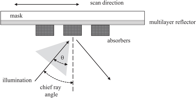
Fig. 1. Schematic of an EUV mask under illumination. Light rays illuminate the mask over a range of angles. The chief ray passes through the center of the illumination cone.
Download figure:
Standard image High-resolution imageTable I. Angles of incidence on masks in EUV exposure systems for various NA's and lens reductions.
| 0.33 NA @ 4× | 0.55 NA @ 4× (est.) | 0.55 NA @ 8× | |
|---|---|---|---|
| Chief ray angle | 6° | 9.2° | 5.3° |
| Largest angle on mask | 10.8° | 17.1° | 9.5° |
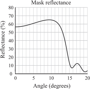
Fig. 2. Reflectance of a Mo/Si multilayer film as a function of the angle of incidence. 3)
Download figure:
Standard image High-resolution imageThis choice of lens reduction, coupled with the decision to stay with the current mask form factor, means that the maximum exposure field size on the wafer is smaller than the current size of 26 mm × 33 mm. Imposing 8× lens reduction in the directions parallel and perpendicular to the plane of incidence would lead to ~¼× field sizes on the wafer, which necessarily would lead to difficulty in making chips with moderately-sized dies and would greatly lower throughput. This problem has been addressed by ASML and Zeiss by maintaining 4× lens reduction in the direction perpendicular to the plane of incidence, resulting in 26 mm × 16.5 mm field sizes for high-NA EUV exposure tools. Lenses with magnifications or reductions that are different between axes are known as anamorphic lenses. Such optics are not unusual, being used often for wide-screen cinematography, 4) but they have not been applied previously to advanced lithography.
The architectural choice of anamorphic lenses reduces the impact on throughput of 8× reduction in the scan direction, but increases the difficulty of lens fabrication. Anamorphic lenses require mirrors that are not rotationally symmetric, necessitating the development of appropriate polishing techniques that meet tight requirements for figure and roughness. High-NA lenses are targeted to have figure accuracy < 20 pm rms. 5) Mid- and high-spatial frequency roughness is currently below 100 pm rms on 0.33 NA lenses, 6) and similar levels will be needed on high-NA lenses to keep flare (scattered light) to acceptable levels.
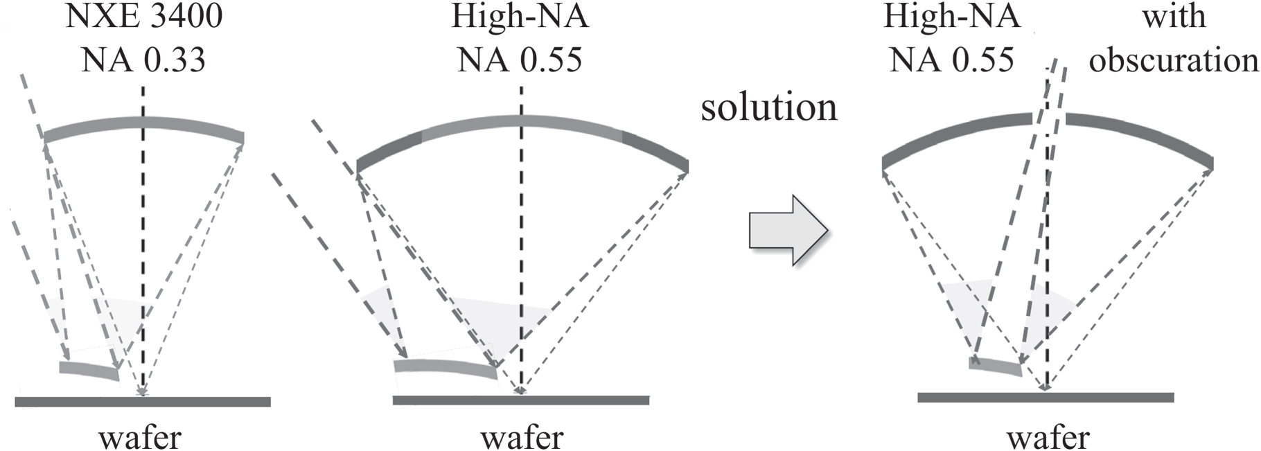
The narrow range of angles of incidence over which multilayer mirrors have high reflectance has implications for lenses as well as masks. Extending the lens design concept for the current generation of 0.33 NA lenses to 0.55 NA results in large angles of incidence of mirror surfaces, which is problematic. Accordingly, Zeiss is using a different type of design for high-NA that reduces the maximum angle of incidence on mirrors. 5,7) (Fig. 3) An essential characteristic of this new design is a central obscuration. High performance lenses with central obscurations have been used for other applications, such as astronomy, the Hubble Space Telescope being a well-known example. 8) With a central obscuration, Zernike polynomials are no longer orthogonal over the pupil, and an alternative set of polynomials (Tatian polynomials) needs to be used to characterize aberrations. 9) Fortunately, the formalism for characterizing aberrations in optical systems with annular pupils is well established. 10)
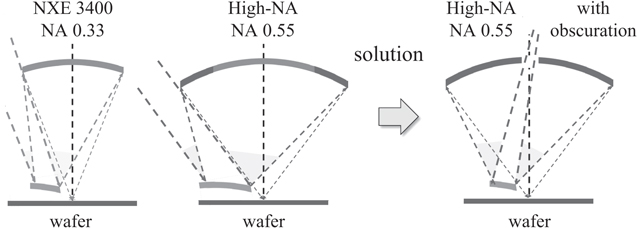
Fig. 3. Illustration of the final two mirrors in EUV lenses. 5) Extension of the lens design used for 0.33 NA EUV lenses to 0.55 NA leads to excessively large angles of incidence. The lens design on the right, with a central obscuration, avoids such large angles, even at high NA.
Download figure:
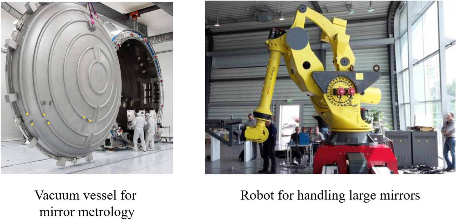
Standard image High-resolution imageIncreasing numerical aperture means that the largest mirror in the lens must also increase in size. A comparison of the largest mirrors in 0.33 NA and 0.55 NA projection optics is given in Table II. As can be seen, the largest mirrors for 0.55 NA lenses are sizable and massive. This leads to some practical issues that have been addressed by Zeiss. First, such massive mirrors cannot be handled manually, necessitating the use of robots, and large robots at that. A picture of a robot at Carl Zeiss in Oberkochen, Germany for handling mirrors during optics manufacturing is shown in Fig. 4. 11) As can be seen by comparison with the people in the picture, this is a large robot.
Table II. Diameters and masses of largest mirrors in 0.33 and 0.55 NA EUV projection optics.
| Diameter of largest mirror | Mass of heaviest mirror | |
|---|---|---|
| 0.33 NA | 0.65 m | 40 kg |
| 0.55 NA | 1.2 m | 360 kg |
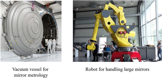
Fig. 4. (Color online) On the left, vacuum vessel in which optics metrology is performed. A robot for handling large EUV mirrors is shown on the right. 5,11)
Download figure:
Standard image High-resolution imageMetrology of EUV optics is typically performed in vacuum. This is absolutely necessary for at-wavelength metrology, since EUV light does not propagate through air, and greater precision is possible in vacuum at optical wavelengths due to elimination of air turbulence-induced measurement noise. Given the size of mirrors for high-NA EUV lithography, the vacuum vessels in which optical metrology is performed are also large (see Fig. 4). The deposition of the multilayer coatings on the mirror's glass, with sub-nanometer control, also must be done in large vacuum systems. 12)
Fully assembled lenses are very complex, consisting of more than 20 000 individual components. 12) Considering the levels of complexity and precision in fabrication and measurement required to make high-NA EUV lenses, coupled with the necessary size of the equipment involved, it can be inferred that substantial financial investments were required to establish the infrastructure needed to make high-NA lenses. This, in turn, has implications for the cost of high-NA EUV lithography, a topic that will be discussed in Sect. 3.8.
For high-NA EUV exposure tools, ASML will use an illuminator that is similar to those used for 0.33 NA systems. (Fig. 5) As with all optical elements for EUV lithography, the mirrors in the illuminator need to be of good quality. Although the quality requirements are not as exacting as for projection optics, each mirror must be fabricated and mounted individually, making for complex production. 13) EUV illumination is broken into hundreds of pixels, an order of magnitude smaller number than found in the illuminators of optical exposure tools 14) because of this manufacturing complexity. The mirrors illustrated in Fig. 5 are movable, enabling the creation of programmed illumination shapes. (Fig. 6) With the current illuminator design, illumination with pupil fill down to 20% can be used without significant loss of light. 15) If it proves important to have illumination with lower pupil fill, the illuminator design can be reconsidered. Since an illuminator that can support high transmission at low pupil fill will likely requires more mirrors, the value of lower pupil fill will need to be balanced against increased fabrication costs.
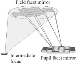
Fig. 5. Schematic of illuminator mirror arrays used in ASML EUV exposure tools.
Download figure:
Standard image High-resolution image
Fig. 6. Examples of pixelated, programmable illumination.
Download figure:
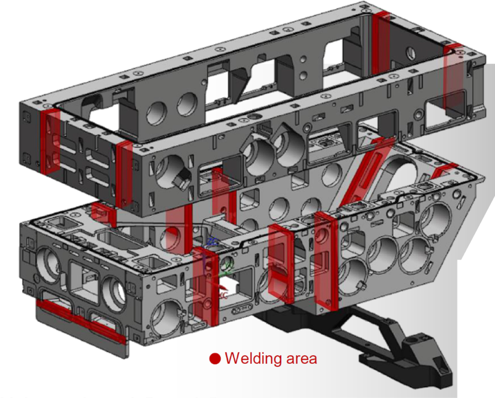
Standard image High-resolution imageThe capabilities established by ASML to build and assemble high-NA EUV exposure tools are equally impressive. For example, to support more precise mechanical motions of wafers and reticles, new electron-beam methods are used to weld the exposure tools' frames so they will be more rigid than in prior generations of exposure systems. An illustration of frame welding is shown in Fig. 7. 16) The dimensions of the frame shown in Fig. 7 are approximately 6 m × 2.5 m × 2.5 m. Electron beam welding must be performed in vacuum, so necessarily done robotically in a vacuum chamber sufficiently large to accommodate the sizeable frame being welded.

Fig. 7. (Color online) Illustration of welding of the frame of ASML high-NA EUV exposure system.
Download figure:
Standard image High-resolution imageAttention to detail regarding frame rigidity is motivated by the more demanding mechanical requirements for high-NA systems, relative to 0.33 NA tools. For example, on all scanning exposure tools the mask scan speed equals the wafer scan speed times the lens reduction. Consequently, the increase of lens reduction from 4× to 8× on high-NA EUV exposure tools means that the mask must scan during exposures at twice the speed of masks on 0.33 NA systems in order to achieve the same wafer scan speed. Wafer scan speeds on EUV exposure tools are currently limited by exposure source power, so they are typically less than the ≥ 800 mm s−1 achieved on optical exposure tools, 17) but mask scan speeds of multiple meters per second are still required. This must be achieved while meeting the sub-nanometer position control required for good overlay and imaging. Moreover, in order to achieve good exposure tool throughput, ASML is targeting a 4× increase in reticle stage acceleration and a 2× increase in wafer stage acceleration. 18)
For the high-NA scanner platform, ASML is using some of the same subsystems that are deployed on 0.33 NA EUV exposure tools, such as wafer and mask handling systems, wavefront metrology, and alignment and focus sensors. 16) Reuse of subsystems benefits scanner uptime and maintainability, since reliability of these subsystems has already been demonstrated, and should they fail, maintenance technicians are already trained in repairing them. Moreover, the supply of replacement parts is streamlined.
ASML will also use laser-produced plasma light sources on high-NA systems, similar to those used on 0.33 NA EUV exposure tools. Such light sources, incorporating CO2 lasers and tin-droplet targets, were developed over the course of several years, 19) and have been used in HVM since 2019. Accordingly, there is considerable experience with such light sources that can be leveraged for high-NA EUV lithography. ASML is continuing to increase the output of LPP sources, and 400–500 W at intermediate focus is currently being achieved, 16) with efforts on-going for even higher light output.
ASML has presented timelines for the introduction of high-NA EUV tools. 20) Their first generation tool (NXE:5000) is projected to be available in 2023, while their second generation tool (NXE:5200) will be ready in 2025. As with prior generations of technology, chip makers can do their process development using early exposure tools, while the next generation of exposure systems will be enhanced for HVM, particularly with respect to productivity. The first sets of high-NA optics are being fabricated at Zeiss, while production of scanner sub-assemblies has started. The first tool built will be installed in Veldhoven, the Netherlands, in a high-NA EUV lithography lab, in cooperation with Imec. 20) ASML's customers will also have access to this tool prior to deliver of high-NA systems to customer fabs in 2024.
3. Key challenges of high-NA EUV lithography
3.1. Overview
While engineers at ASML and Zeiss are addressing the technical issues associated with designing and fabricating high-NA EUV exposure tools and optics, there are several other issues of concern to lithographers at the chip companies who need to create integrated patterning solutions. A summary of some of the key challenges are listed in Table III. 21,22) These are important considerations, since all elements of a lithographic process must be capable in order for the process to be useable in manufacturing. More detail on these challenges is provided in the remainder of this section.
Table III. Key challenges of high-NA EUV lithography.
| Key challenges |
|---|
| Resists meeting resolution requirements, with low levels of defects from stochastic phenomena and pattern collapse |
| Light sources that can support photon shot noise and productivity requirements |
| Solutions for meeting small depths-of-focus at 0.55 NA |
| Polarization control for maintaining high contrast at 0.55 NA |
| Computational lithography capabilities |
| Mask making and metrology infrastructure |
| Solutions for large dies |
| Cost of high-NA EUV lithography |
3.2. Resists meeting resolution requirements
Resists have long been limiting the capabilities of EUV lithography, 23) and with demands for increased performance to meet the requirements of scaling, resists are expected to continue to be a constraint for EUV lithography, even with continuing advances in lithographic materials. Early in the development of EUV lithography, it was recognized that resolution was being limited by photoacid diffusion during post-exposure bake. 24) Steps were taken by resist manufacturers to reduce photoacid blur, leading to resists with improved resolution. Later, it became appreciated that the resolution of EUV resists can also be limited by photoelectron and secondary electron blur. 25,26)
It was also understood that line-edge roughness (LER) limited the applicability of EUV lithography. 27) LER is not something that can be predicted by means of continua models, for it is fundamentally a quantum phenomenon. While LER was recognized initially as relevant to optical lithography, 28) it became an issue of greater concern to EUV lithography due to several factors. First, the small size of features targeted for patterning by EUV lithography meant that levels of LER that were of small consequence for optical lithography became very significant for EUV lithography. Moreover, the weakness of EUV light sources motivated lithographers to attempt to minimize exposure doses, which resulted in a sizable contribution of photon shot noise to LER. 29) Studies of LER later led to recognition that stochastic variations cause defects as well as roughness. 30) (Fig. 8) While LER and defects due to stochastic mechanisms are not issues specific to high-NA EUV lithography, they are highly relevant, since high-NA is expected to be used to pattern devices with many transistors, necessitating a decrease to very low defect levels, and small features will require low LER.
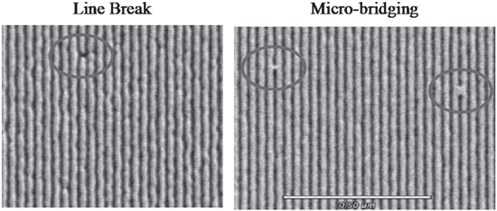
Fig. 8. Examples of stochastics-induced defects in 30 nm lines/spaces patterned using EUV lithography.
Download figure:
Standard image High-resolution imageAs features have continued to scale, the sizes of resist molecules have become non-negligible fractions of critical dimensions. At the molecular level, resist materials are not homogeneous. Inhomogeneity can result from randomness, component segregation and aggregation (Fig. 9). When photoacid generators (PAGs) are not bonded to the resist polymers, PAG-PAG spacings will be variable. For a resist with high PAG loading, the average PAG-PAG spacing is 1.7 nm, 31,32) which sets the scale for roughness. Variation in component spacings can be increased beyond that expected from pure randomness due to the phenomena of segregation and aggregation. PAGs are polar molecules, so they can attract each other (Fig. 10), resulting in aggregation. With aggregation, the effects of resist inhomogeneity are increased. 33) Base quenchers are subject to similar variability in distribution.
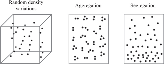
Fig. 9. Examples of mechanisms that lead to homogeneity at the molecular level.
Download figure:
Standard image High-resolution image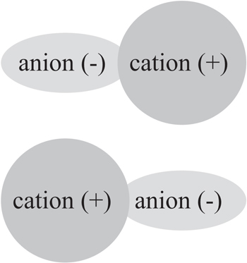
Fig. 10. Photoacid generators (PAGs) as polar molecules, which can lead to aggregation.
Download figure:
Standard image High-resolution imageSegregation in resists has been observed, particularly in ultrathin resist films, even though the mechanisms causing segregation are not yet well understood. Gradients of photoacids from the top to bottom of resists films were inferred from simulations, where observed results could not be explained through models that assumed uniform distributions of photoacids. 34) More recently, segregation in resist films has been measured directly using resonant soft X-ray reflectivity (RSoXR), 35) where data were inconsistent with models that assumed resist material homogeneity. On the other hand, models could be fit well to data if the resist was assumed to consist of three layers of differing composition. (Fig. 11) The problem of segregation becomes increasingly significant as resist films become thinner. At the dimensions of interest for high-NA EUV lithography ultrathin resist films are needed to mitigate pattern collapse. Moreover, as will be discussed in Sect. 3.3, ultrathin resist films will be needed to address small depths-of-focus, making these issues of particular importance for high-NA EUV lithography.
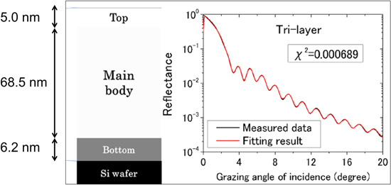
Fig. 11. (Color online) Resonant soft X-ray reflectivity measurements. The thickness of the layers comprising the resist film, determined by fitting the model to the data, are shown on the left. 35)
Download figure:
Standard image High-resolution imageIn addition to the spacing between components, there are other factors that set the length-scale for roughness in resist patterns. Resist films are made of molecules, which are of finite size. For many years, the size of resist molecules was considerably smaller than minimum device features, so the detailed structure of resists was not relevant to process control. LER became a subject of interest around the same time that ArF lithography was being introduced, although it was then having only a small impact on process control. As features continued to shrink below 100 nm, LER began to affect linewidth control and device performance. 36–39) Relative length scales for 10 nm ½-pitch technology are shown in Fig. 12. 40) As can be seen, process control requirements for high-NA EUV lithography are similar in size to the molecules that comprise resists.
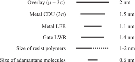
Fig. 12. Comparative length scales of patterns and resist molecules. Adamantane is a chemical often appended to resist polymers to increase etch resistance. The values for LER and LWR are taken from the More Moore tables of the 2021 IRDS. 40)
Download figure:
Standard image High-resolution imageChemically amplified resists based on photoacid-induced deprotection are also prone to pattern collapse at tight pitches. 41) Considerable effort has been expended to mitigate pattern collapse, but the problem appears to persist at ½-pitches less than 12 nm. Accordingly, pattern collapse is a major issue at the dimensions of interest for high-NA EUV lithography. A detailed understanding of the mechanical properties of resist materials also requires considerations at the molecular level. The results of nanoscopic mechanical calculations of the C33 component of the local elasticity matrix for resist patterns are show in Fig. 13. The outer layers of the features shown in this figure have lower rigidity than the bulk material, resulting from greater free volume for material on the free surface. 42,43) The fraction of the feature volume composed of this lower rigidity material increases as shapes get smaller, which leads to greater susceptibility to pattern collapse and a need to reduce aspect ratios (height/width).

Fig. 13. (Color online) Results of mesoscale simulations of the C33 component of the local elasticity matrix for patterned chemically amplified resist. 42,43) Values are given as percentages of bulk values.
Download figure:
Standard image High-resolution imageOne resist issue that appears to be common to all resist material platforms is blur. The radiation chemistry in EUV resists is driven by photoelectrons that are generated by the absorption of EUV photons, and from resulting secondary electrons, rather than directly from the photoabsorption event. This appears to be a characteristic common to many different types of EUV resist platforms. Understanding the impact of electron blur requires knowledge of the minimum energy at which the secondary electrons can cause a radiation chemistry event and the ranges over which these electrons travel before they scatter and have insufficient energy to induce chemical reactions. This is currently a topic of active research. 44) Current estimates for the distances from the initial photoabsorption over which secondary electrons can induce chemical events is ∼3 nm, 45) although there are uncertainties to these quantities, which are also dependent on resist material composition. In addition to image blur due to electrons, there is additional blur in chemically amplified resists due to photoacid diffusion during post-exposure bake.
The net result of electron scattering and photoacid diffusion is blur, but these phenomena have statistical characteristics that become significant when there are a small number of events. Consider photoacid diffusion. Individual photoacids will undergo random walks, on-average resulting in blur. (Fig. 14) Electron scattering is similar, though more complicated, because scattering events can result in production of additional secondary electrons. 26) Although the probability is very low, there can be situations where random walks go in one general direction, which can lead to defects. 6,46) Since defect levels need to be sub-parts-per-billion, very low levels can reduce yield.

Fig. 14. Random walk diffusion of a photoacid, resulting in resist deprotection. On average the net effect is blur.
Download figure:
Standard image High-resolution imageNew types of resist have the potential to overcome many of the issues seen currently with chemically amplified resists. For example, metal-oxide resists, upon exposure lead to networks of cross-linked structures. 47) This cross-linking can increase rigidity, thereby reducing pattern collapse. Another type of resist is based upon the scissioning of polymers. The products of resist scissioning are smaller than the original polymers, reducing the scale for roughness at the molecular level. ZEP520A, an electron-beam resist, is an example of a scissioning resist, and there are currently efforts to optimize this resist platform for application to EUV lithography. 48)
Development of resists targeting 10 nm ½-pitch and below is proceeding. This includes efforts to extend chemically amplified resists as well as the development of alternative platforms. However, resists with low LER, low levels of stochastics-induced defects, no pattern collapse, and the requisite resolution, while avoiding excessively high exposure doses have not yet been found. Improvements in resists will be needed to enable fully high-NA EUV lithography.
3.3. Light sources that can support photon shot noise and productivity requirements
Regardless of resist platform or specific formulation, there is a dose below which the photon shot noise induced LER and defects are too large to meet technology requirements. In the 2021 International Roadmap for Devices and Systems, it is projected that doses slightly greater than 80 mJ cm−2 will be needed to support 10 nm half-pitch patterning. 49,50) This necessitates light sources with sufficiently high output power to avoid low throughput and productivity. This problem is illustrated in Fig. 15. 51) If we assume a 500 W source and exposure dose of 80 mJ cm−2, then the throughput for a 0.55 NA tool will be 120 wafers h−1, substantially less than the 185 wafers h−1 that occurs when the source power is high enough for throughput to be limited by mechanical considerations only. Such a limitation would occur for source powers of approximately 1.3 kW or higher if the exposure dose is 80 mJ cm−2.
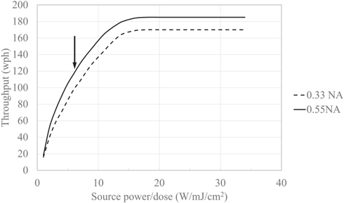
Fig. 15. Throughput for ASML's EUV exposure tools as a function of source power (W) divided by the exposure dose (mJ cm−2). 51) These throughputs are based on an assumption of 96 shots/wafer for 0.33 NA tools and 188 shots/wafer for 0.55 NA systems. The arrow indicates the point for a tool with a 500 W source and 80 mJ cm−2 exposure dose.
Download figure:
Standard image High-resolution imageASML San Diego has achieved 400–500 W output with their laser-produced plasma (LPP) light source. 16) Increases in the output of LPP sources have been achieved through higher efficiency in converting infrared laser light to in-band EUV light, as well as improvements in pulse-to-pulse repeatability. As efficiency and repeatability approach possible maxima, further increases in LPP light output can be achieved through the use of higher power infrared lasers.
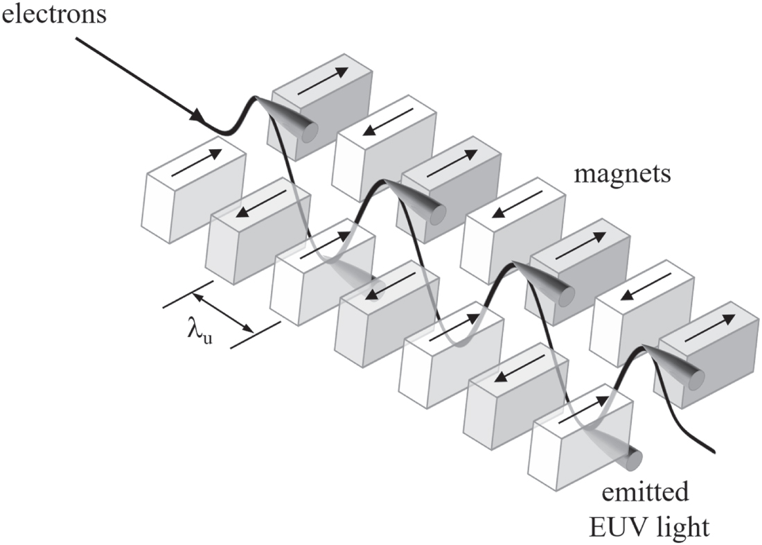
Free-electron lasers are being considered as alternatives to LPP light sources. Such sources of light are based on particle-accelerator technology. Electrons that are near the speed of light are injected into an array of magnets (Fig. 16), where the oscillating electrons emit light of wavelength λ, given by the following expression 52):

where

where B0 is the peak magnetic field in the magnet array, m is the mass of an electron, c is the speed of light, and γ is the relativistic factor:

A magnet array with a period of 2 cm, with 800 MeV electrons, can produce 13.5 nm EUV light. 53) A cavity with gain can be produced by placing annular mirrors at both ends of the magnet array. 54) Free-electron lasers have been made at infrared and other wavelengths, and research on such lasers at EUV wavelengths is being conducted. 55,56) Although free-electron lasers comprise a substantially different class of light sources than used currently for EUV lithography, they represent a potential long-term path to very high source source power.
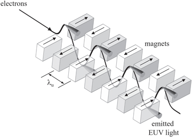
Fig. 16. Illustration of a magnet array used to oscillate an electron beam transversely to the primary beam direction, resulting in the emission of EUV light. Arrows indicate the direction of the magnetic field.
Download figure:
Standard image High-resolution image3.4. Solutions for meeting small depths-of focus at 0.55 NA
Focus control has long been a challenge for optical projection lithography. 57) At NA = 0.55, the Rayleigh depth-of-focus (DOF) is


which is about 1/3 that of 0.33 NA tools. With resolution enhancement techniques, depths-of-focus greater than the Rayleigh DOF are possible, but it will remain the case that the DOF decreases substantially as the NA increases from 0.33 to 0.55. Accordingly, much improved focus control will be needed to enable high-NA EUV lithography.
To obtain good imaging, a quality aerial image is needed throughout the depth of the resist. In optical lithography, this is facilitated by refraction that occurs at the air-resist or water-resist interface. (Fig. 17) The relationship between θ1 and θ2 is given by Snell's law:

where nresist is the index of refraction of the resist and nair/water/vacuum is the index of refraction of the medium above the resist. Larger values for nresist lead to greater depth to which acceptable blur can be attained. However, for EUV lithography, the real part of the index of refraction for most materials is close to 1.0 and is often < 1.0. This means that refraction of EUV light is small, and to the extent that there is refraction, it decreases the depth over which the blur is acceptable. As a consequence of the small optical depth-of-focus, coupled with the lack of mitigation by refraction, it will be important to have very thin layers of resist for high-NA EUV lithography. As discussed in the previous section, there are phenomena, such as component segregation, that degrade patterning significantly as resist films become very thin.
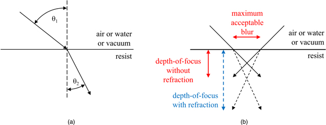
Fig. 17. (Color online) (a) Refraction at the top surface of the resist. (b) Illustration of how refraction at the top of the resist film increases the depth through which acceptable image blur is achieved.
Download figure:
Standard image High-resolution imageFocus control is not a problem solely within lithography. Excellent wafer flatness will also be required, starting with bare silicon wafers and continuing through wafer processing. This places tight requirements on film deposition and particularly on chemical-mechanical polishing (CMP). Substrate uniformity will help with focus control, but focus sensors that are very insensitive to substrate films will also be needed.
3.5. Polarization control for maintaining high contrast at 0.55 NA
At high numerical aperture, image contrast is dependent on polarization of the illumination. 58) As shown in Fig. 18, image contrast of two interfering plane waves can be maintained with large NA with S-polarized light, but contrast becomes smaller with P-polarized and unpolarized light as the NA is increased. For this reason, the illumination systems of advanced immersion scanners provide polarization control. 59) The laser-produced plasma (LPP) light sources planned for initial use on high-NA exposure tools produce unpolarized light. As can be seen in Fig. 18, there can be appreciable loss of image contrast at 0.55 NA with unpolarized light. Polarizing the light involves loss, which would exacerbate all issues associated with low source power. On the other hand, the emission of free-electron lasers is polarized, giving additional motivation to consider free-electron lasers (FELs) as sources for high-NA EUV exposure systems.
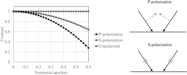
Fig. 18. Contrast of images produced by two interfering plane waves at the largest angles of incidence support by given numerical apertures. For S-polarization, the polarization vectors are perpendicular to the plane of incidence, while they lie in the plane of incidence for P-polarized light.
Download figure:
Standard image High-resolution imageThe reduction of image contrast with unpolarized light is another problem that is mitigated in optical lithography by refraction at the top surface of resist. Since there is no such benefit for EUV lithography, the degradation of contrast for unpolarized illumination occurs at a lower NA than occurred for optical lithography. Fortunately, for the initial applications of high-NA EUV lithography, light rays at the largest angles supported by the numerical aperture will not be essential, so the problem of image contrast loss with unpolarized light will not be a problem at first.
3.6. Computational lithography capabilities
For EUV lithography, computational accuracy requires consideration of many physical phenomena, all of which need to be addressed simultaneously (Table IV). 60) Although this complexity precedes high numerical aperture, greater accuracy is required for high-NA because of the smaller feature sizes of interest for high-NA EUV lithography. Moreover, the small depths-of-focus associated with high-NA increase the demands on computational solutions.
Table IV. Phenomena and requirements that need to be addressed in order to achieve accuracy in computations for EUV lithography.
| Phenomena | Requirements |
|---|---|
| Conventional OPC considerations | CDs within specifications over a suitably large process window |
| Mask error enhancement factor (MEEF) < 4 | |
| Mask 3D effects | Differences in best focus through pitch |
| Imaging blurring | |
| Pattern placement shifts with focus | |
| Resist models | Capturing complex physics into computationally efficient models |
| Stochastics | Need to maintain large NILS |
| Aberrations | Address across slit, tool-to-tool |
| Out-of-band light and flare | Incorporate into OPC models |
In Fig. 19, an example is shown of how computational lithography can be used to improve patterning. 61) Illumination in one case (Low DOF) has maximum normalized image log-slope (NILS) at best focus, while another illumination has lower NILS at best focus, but constant NILS through focus (Iso NILS). As can be seen in Fig. 19, considerably reduced pattern collapse was seen with the Iso NILS illumination.
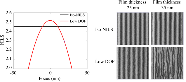
Fig. 19. (Color online) Images of 16 nm lines and spaces, patterned using different illuminations. 61) The low DOF illumination was designed to maximize NILS at best focus, while the Iso NILS illumination provides the same NILS value throughout focus.
Download figure:
Standard image High-resolution imageInverse lithography technology (ILT) is a technique that has proven useful for constructing mask layouts that maximize process windows. 62) Until recently, because of long computation times, the application of ILT has been limited to addressing hotspots or memory cells. Moreover, optimum mask layouts resulting from the application of ILT have often been curvilinear, which has made it difficult to fabricate the masks. There has been much recent progress to enable ILT fully. GPU-acceleration has reduced computation times significantly, enabling the application of ILT to full-chip layouts with practical computation times. 63–65) Multibeam mask writers have made it possible to produce high quality masks with curvilinear patterns, 66) and an initiative has started to standardize data formats for curvilinear features on masks. 67) With capability established for writing masks with curvilinear features with reasonable write times and pattern quality, other elements of mask-making relevant to the fabrication of such masks are being addressed. In terms of EDA infrastructure, software for mask process corrections (MPC) 68) and mask rules check (MRC) 69,70) need to be adapted for application to curvilinear features.
ILT and curvilinear features are not unique to high-NA EUV lithography, but these hcapabilities are coming to maturity in the same time frame that high-NA EUV tools will become available. Consequently, these approaches can be expected to be important elements of high-NA technology. These techniques may also prove useful for extending 0.33 NA EUV lithography, and so could affect the timing for the introduction of high-NA EUV lithography into HVM.
3.7. Mask making and metrology infrastructure
From the perspective of high-NA EUV lithography, there were a number of fundamental mask issues, preceding those discussed in the prior section, that needed to be addressed early in the development of high-NA lithography. Because of ASML's decision for high-NA EUV masks to have the same mechanical form factor (152 mm × 152 mm × 6.35 mm) as those used currently for 0.33 NA EUV and advanced optical lithography, the tools for making high-NA EUV masks can be the same ones as used currently, at least with modest improvements. This greatly simplifies mask making for high-NA EUV lithography. Given the length of time needed to create a complete mask-making infrastructure for masks with a different format (such as 230 mm), 71) it is likely that the development and eventual insertion of high-NA EUV lithography would be gated at many steps by mask availability. Although there are some disadvantages to using 152.mm × 152 mm × 6.35 mm substrates for high-NA EUV lithography, particularly those discussed in the next section, the decision to stay with this form factor was a practical one.
Tantalum-based absorbers for EUV masks enabled the development of EUV lithography and its initial use in HVM. 72–74) However, with dimensions shrinking, mask 3D effects are becoming increasingly significant when such absorbers are used. 75) Alternative mask architectures have been considered, 76) but most recent effort has gone into identifying new mask absorbers for both binary and attenuated phase-shifting masks (attPSM). 77) For binary masks, mask 3D effects can be reduced by having the real part of the index of refraction of the absorber be close to 1.0, while the extinction coefficient (k = imaginary part of the index of refraction) should be as large as possible. This latter condition enables the use of thin absorbers.
For attenuated phase-shifting masks, the desired phase can be achieved with thinner absorbers when the real part of the absorber's refractive index differs significantly from 1.0. 6) Since it is desirable to have an appreciable amount of reflection from the absorber on an attPSM, the absorber should have a moderate extinction coefficient. This means that candidate elements for the absorbers of attPSMs should be those in the lower left corner of Fig. 20, although they may be alloyed with other elements. Since rhodium is an extremely rare element, all isotopes of technetium are radioactive, and there is a dearth of volatile compounds of palladium, absorbers for attenuated phase-shifting masks need to contain substantial amounts of ruthenium. This has implications for the capping layer, which has long been composed of ruthenium, since the capping layer has also provided etch selectivity to the absorber. Accordingly, use of absorbers containing a significant amount of ruthenium will also require an alternative capping layer.

Fig. 20. Indices of refraction for selected elements, primarily metals. The horizontal axis is the real part of the indices of refraction, while the vertical axis is the imaginary part (extinction coefficient). The lower left corner, bounded by dotted lines, is the area for which reflection from the absorber is ≥ 6% of that from the multilayer and absorber thicknesses are ≤ 50 nm.
Download figure:
Standard image High-resolution imageBecause mask absorbers need to meet a large number of requirements (Table V), identification of suitable materials is challenging. 78) Ruthenium is a material known to meet all requirements, and attPSM development has been progressing well. 79) Identification of a suitable material for a high-k absorber has proven to be more challenging, but development is proceeding. 78)
Table V. Requirements for EUV mask absorber materials.
| Characteristics | Requirements |
|---|---|
| Deposition | Single phase |
| Amorphous films | |
| Low surface roughness | |
| Low residual stress | |
| Processing | Cleaning durability |
| Etchable | |
| Repairable | |
| Inspectable | |
| Additional characteristics | Good adhesion to the capping layer |
| Ultrahigh vacuum compatible | |
| Stable to maximum processing temperatures | |
| Hydrogen resistant with and without EUV light |
Attenuated phase-shifting masks are being developed long after the first integrated devices were fabricated using EUV lithography. 80) This delay was due in large measure to the difficulty in finding theoretical solutions. For example, it was only recently understood that the ideal phase shift for EUV attPSMs is not 180° = π as in optical lithography, but is closer to 1.2π. Moreover, optimum solutions may be pitch-dependent. Identifying theoretical solutions is being pursued in parallel with the development of attPSM mask blanks. 81)
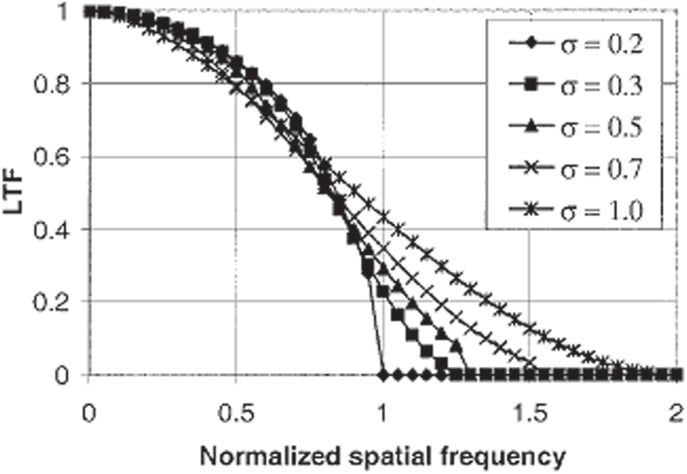
Alternative mask absorbers are discussed in the context of high-NA EUV lithography, primarily because they will become available at roughly the same time as high-NA tools, and not because they are necessarily integral or specific to high-NA. Roughness is another aspect of masks that is relevant for 0.33 NA EUV lithography as well but is much more significant for high-NA. The extent to which absorber edge roughness transfers from mask to wafer is dependent on lens resolution, as higher spatial frequency roughness will transfer at larger NA. 82) (Fig. 21) Similarly, mask multilayer roughness, which has been shown to have a measurable, but not large impact on local dose variation for 0.33 NA optics, 83) appears to be more significant for high-NA EUV lithography. 84)

Fig. 21. LER transfer function, from mask to wafer, as a function of spatial frequency, normalized to NA/λ⊡ 82)
Download figure:
Standard image High-resolution imageThe use of anamorphic lenses necessitates commensurate dimensional changes on the masks. The 8× reduction relaxes dimensions along one axis, but dimensions along the other axis will be sized 4×. Since patterning, inspection, and measurement requirements are driven by the smallest features, much mask making technology will continue to be driven by a continuation of scaling requirements. For inspecting patterned high-NA EUV masks, Lasertec has been developing an extension of their ACTIS A150 actinic patterned mask inspection tool, 85) with higher resolution optics and different resolution scales in the x- and y-directions. Additionally, die-to-database algorithms, suitable for the asymmetric configuration of high-NA, are being developed. These algorithms will also need to be ultimately capable of handling curvilinear features.
3.8. Solutions for large dies
Integrated circuits with very large die sizes have become important products. Integrated circuits such as the Nvidia GA100 GPU and Intel Skylake processors are so large that only one die can fit in a 26 mm × 33 mm exposure field, and such devices are too large to fit in the ½-field of high-NA exposure tools. In order to continue producing devices with similar chip sizes, stitching will need to be adopted. With stitching, part of the chip layout is patterned using one mask, while the remainder is patterned by exposure of a second mask (Fig. 22).
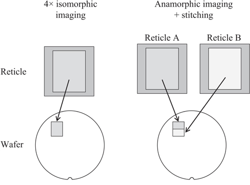
Fig. 22. Illustration of imaging with 4× isomorphic imaging and 4×/8× anamorphic imaging.
Download figure:
Standard image High-resolution imageStitching is not a new lithographic technique, having long been an element of electron-beam lithography, and it has also been used in optical lithography for the production of large-area devices. 86) However, very precise implementation is necessitated by the tight process control requirements of the nodes at which high-NA EUV lithography will be applied. There are also special considerations that apply to EUV lithography. For example, flare (scattered light) is significantly higher in EUV lenses than optical lenses. As a consequence, scattered light from the exposure of one sub-field can expose resist in the area allocated to the other sub-field, with a range of microns. Another set of issues arises from the black border on EUV masks. Because EUV absorbers are not fully effective in suppressing reflected light, the multilayer reflector around the exposure area on the reticle is often removed by etching (Fig. 23). Mo/Si multilayers have 100–500 GPa stress. 87) Etching the black border leads to locally reduced stress, which can displace mask features. 88) The results of careful measurements performed at Imec of pattern displacement are shown in Fig. 24. 89)
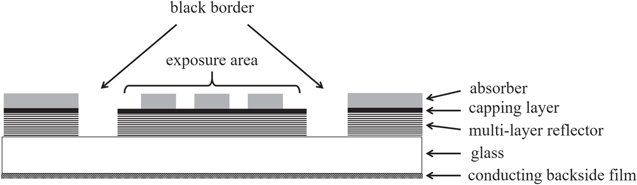
Fig. 23. Illustration of an EUV mask with an etched black border.
Download figure:
Standard image High-resolution image
Fig. 24. (Color online) Pattern placement errors near an etched black border. 89)
Download figure:
Standard image High-resolution imageIn addition to pattern placement errors, there can be aerial image cross-talk across the stitch boundary, as well as variations in flare due to different pattern densities on the two sides of the boundary. These phenomena that affect critical dimensions can be compensated through OPC, and pattern placement errors can also be corrected by calculating the displacement due to stress reduction and compensating during mask writing. Because the magnitude of these effects is greatest near the stitch boundary and the accuracy of such corrections may become inadequate very close to the boundary, a 1 μm exclusion zone between sub-fields has been proposed. 89) While such an exclusion zone will have little impact on the number of dies/wafer, it does preclude geometries that cross stitch boundaries, such as interconnects. Fortunately, the tightest pitch metal layers are usually confined to logic and memories cells and local routing. These can be done with high-NA EUV lithography, while the routing that needs to cross stitch boundaries can be patterned using 0.33 NA EUV lithography. It is also reasonably straightforward to avoid having contacts and vias within this exclusion zone. The special issues associated with stitching provide additional motivation for using multiple patterning with 0.33 NA exposure tools rather than high-NA EUV lithography, particularly for across-die routing.
An alternative solution is the avoidance of large dies altogether. With advanced packaging, it has proven possible to maintain high performance even while separately fabricating parts of circuits that previously had been fully integrated into a single die. 90,91) This is currently being done to improve the cost-effectiveness of advanced lithography. 92) For example, the high performance logic circuits of AMD's Epyc processor have been fabricated using 7 nm technology, while input/output functions were fabricated using lower cost 14 nm processes. 93) In other applications, memory access rates are improved using advanced packaging technology. 94) It may also be possible to achieve high levels of performance with maximum die sizes that can fit into the exposure fields of high-NA EUV exposure tools.
3.9. Cost of high-NA EUV lithography
As described in Sect. 2, high-NA EUV exposure tools will be complex, and fabrication will require exceptional attention to detail. As a consequence, high-NA EUV exposure tools are expected to cost in excess of $300 M. 95) Over many prior generations of exposure tools, the exponential increase in prices was offset by improvements in throughput, 96) and with high capital costs for high-NA EUV tools, throughput will be especially important.
The projected throughput of first generation high-NA EUV exposure tools, as a function of source power divided by exposure dose, was shown in Fig. 15. For low source power or high exposure doses, the throughput is less than the maximum, which is limited by the mechanical capabilities of the system. Source power of 400–500 W has been achieved by ASML San Diego for LPP sources, with apparent plans for even higher power. In the 2021 IRDS, for the "2.1 nm" node, which will involve a 20 nm minimum metal pitch and be in production in 2025, exposure doses of 80 mJ cm−2 are predicted. With >800 W sources, the throughput of high-NA EUV exposure tools will be close to the mechanical limit.
The throughputs of Fig. 15 are based on an assumption of 96 shots/wafer for 0.33 NA tools and 188 shots/wafer for 0.55 NA systems. In wafer fabs, the number of shots per product wafer is usually greater than the number of shots on which exposure tool suppliers' throughput specifications are based, so actual throughputs in production will be less than those indicated by the graph of Fig. 15. In one study, actual die sizes were used to determine the number of shots per wafer for high-NA EUV tools, resulting in the distribution shown in Fig. 25. 97) In all cases the number of shots per wafer exceed 188, and for several die sizes, the number of shots per wafer was more than twice that amount. With more shots per wafer than assumed for the throughputs shown in Fig. 15, scanner throughput in production will generally be lower than those in the graph.

Fig. 25. Histogram of the number of products versus shot count using real die sizes in a foundry, but assuming a 26 mm × 16.5 mm exposure field.
Download figure:
Standard image High-resolution imageBesides requiring more shots per wafer, there additional ways in which short exposure fields increase the difficulty of attaining high throughputs. In scanning, the reticle and wafer stages are accelerated until they reach the proper scanning speed, which needs to occur before the top part of the slit begins to expose the wafer, and it continues until the bottom part of the slit no longer is exposing the wafer. (Fig. 26) Thus, the total scanning distance is longer than the field height HF by an amount Δ. This constraint is true on optical scanners, but the extra scanning distance Δ on EUV tools is made longer by the curvature of the slit. The scan time texp is given by

where S is the exposure dose and  is the average light intensity across the slit. If we assume that high-NA tools will have the same slit height H and curvature as 0.33 NA tools, then scanning the distance Δ takes approximately ¼ of the total scan time, double what is necessary on 0.33 NA tools. With half-height exposure fields, it will be challenging to attain cost-effective throughput for high-NA EUV exposure systems.

Fig. 26. Illustration of scanning with a curved slit.
Download figure:
Standard image High-resolution image
Reliability and maintenance also affect the cost-effectiveness of lithography. Equipment downtime directly reduces tool output, while maintenance costs include the cost of replacement parts and wages for service technicians. Reliability and maintenance costs of high-NA exposure systems are being mitigated by ASML's decision to incorporate certain modules, such as wafer and mask handlers, that are used in their 0.33 NA tools. The use of identical modules will take advantage of past reliability improvements and reduce costs for stocking replacement components. Many years of experience with laser-produced plasma light sources can be applied to high-NA, accelerating the time to achieve high uptime.
Cost has always been a concern of lithographers, and it will certainly be a challenge for high-NA EUV lithography. Higher power light sources will be beneficial. In addition to providing polarized light, free electron lasers are expected to have high power, so cost is another reason for free electron lasers to be given consideration as sources for EUV exposure tools.
4. Timing for the implementation of high-NA EUV lithography
Adoption of a new lithographic technology takes place when the following conditions are all met:
- 1)There is a need for the new technology.
- 2)Technical solutions exist or will exist when needed.
- 3)The new technology is cost-effective.
According to the IRDS, 3 nm logic technology is expected to go into production in 2022. The minimum metal pitch of 24 nm for this node represents k1 = 0.29 for 0.33 NA imaging, so it is resolvable optically. However, such a low k1 may not be achievable due to mask 3D effects and resist stochastics. Since high-NA EUV exposure tools will not be available in 2022, multiple patterning will be required for the 3 nm node.
The next node (2.1 nm) in the IRDS occurs in 2025, with a minimum metal pitch of 20 nm. High-NA EUV exposure tools for use in HVM are expected to be available by 2025. Moreover, pre-production tools should be available in 2023, two years earlier and when chip makers will need to start their 2.1 nm technology development. However, high-NA exposure tools are not expected to be operational in wafer fabs until 2024. This leaves only one year to develop 2.1 nm wafer processes for HVM in 2025, which is less time than is typically required to bring processes to sufficient maturity. Chip makers have several options. One is to start 2.1 nm process development using multiple patterning with 0.33 NA EUV tools, and then shift to high-NA in the second year of technology development. Such a transition could also take place after 2.1 nm manufacturing has started.
In addition to the availability of exposure tools, there are a number of factors that will determine whether or not high-NA EUV lithography is actually used for the 2.1 nm node. For the key challenges listed in Table III, what is required for development is somewhat different than what is needed for manufacturing. For example, throughput and cost considerations are considerably less demanding for development than for HVM. With existing light sources (500 W) and resists requiring exposure doses of 100 mJ cm−2, a scanner throughput of over 100 wafers per hour can before inferred from Fig. 15. Even with some moderate degradation of throughput due to more shots/wafer than assumed for Fig. 15, the throughput should still be adequate for supporting technology development at chip companies.
There are several other key challenges that have relaxed requirements for development, relative to HVM, off-setting the shorter time available to attain readiness. For example, good progress can be made during technology development with a reduced set of pitches and simple layouts, easing computational lithography requirements. Test chips for development are usually composed of small blocks, obviating stitching. Development of the infrastructure for curvilinear features and new mask materials is proceeding well, and it is expected that these will meet the needs for development and will continue maturing to meet the requirements of production by 2025. For the first application of high-NA EUV lithography, polarized light will not be needed, so this issue will not hinder insertion.
One parameter that has similar requirements for wafer technology development and manufacturing is focus control, since good imaging is needed even at the beginning of development. There is some uncertainty as to whether or not wafer flatness control and focus control will be adequate by 2023 to meet the needs of 2.1 nm node R&D. Resists also need to meet resolution requirements for the target node at the start of technology development, although defect requirements can perhaps be relaxed somewhat. It may be necessary to use non-chemically amplified resists (CARs) to meet requirements, and this will be a substantial change in lithographic technology, as CARs have been the workhorse resist platform for leading-edge lithography for nearly three decades. Given the need for considerable improvement in resists, it isn't certain that EUV resists will meet requirements for 2.1 nm node development by 2023.
By the end of technology development, sufficient throughput will be needed to meet cost requirements for manufacturing, and there is uncertainty about whether or not source power and resists with suitable resolution and defect densities will be ready for manufacturing by 2025. Similarly, focus control could continue to be a significant challenge. Polarization control will only be needed for generations of technology with pitches well below 20 nm, so it will not be an issue for initial insertion of high-NA EUV lithography, even if a concern for later nodes. Regardless of the exact timing, in spite of concerns, it is expected that the technical challenges will be addressed successfully, and high-NA EUV lithography will be used in HVM.
5. Conclusions
Technology development of high-NA EUV lithography is well underway, with insertion into HVM targeted for 2025. In many ways, high-NA EUV lithography is an evolutionary extension of 0.33 NA EUV lithography, but it will nevertheless be extremely challenging. For the optics, very large mirrors will need to be fabricated with exceeding good surface figure and low roughness. Significant advances in mechatronics are need to simultaneously meet throughput and overlay requirements. The creation of high-NA EUV exposure systems will be a remarkable engineering achievement.
Half-height exposure fields represent a notable departure from prior generations of lithography, since fabrication of chips at sizes that today are commonplace and will require stitching using high-NA EUV lithography or disaggregation. Although stitching has been used in optical lithography, it will be a challenge because of the black border and much tighter process control requirements for the nodes at which high-NA EUV lithography will be used. The smaller field size also increases the difficulty of achieving high throughput and cost-effectiveness. The other approach for addressing half-height exposure fields, disaggregation, will need to be considered at the level of chip design.
Several other elements of lithographic technology, particularly resists and focus control, will need significant improvement from current levels of performance, even to meet the requirements of wafer technology development. For manufacturing, it will be important to have light sources with adequate power to achieve sufficient exposure tool throughput to offset high capital costs. Ultimately, polarized light will be needed to reach the full imaging entitlement of 0.55 NA optics. Significant advances in mask making, mask materials, and computational lithography will also be required. In short, there are many interesting and challenging problems for engineers to solve in order to enable high-NA EUV lithography. However, the creators of lithographic technologies have always faced challenges with every new generation of technology and have addressed them successfully. With this demonstrated record, there is good reason to be optimistic that high-NA EUV lithography will be similarly successful.
Acknowledgments
I would like to thank the following people for permissions to include their figures in this paper: Dr. Sudhar Raghunathan of Hermes Microvision (Fig. 2), Dr. Jan van Schoot of ASML (Figs. 3, 4, 7, and 15), Dr. Claus Zahlten of Carl Zeiss (Fig. 5), Dr. Yulu Chen of Synopsys (Fig. 6), Prof. Takeo Watanabe of University of Hyogo (Fig. 11), Prof. Juan DePablo of the University of Chicago (Fig. 13), Dr. Jara Santaclara of ASML (Fig. 19), Dr. Patrick Naulleau of Lawrence Berkeley National Laboratory (Fig. 21), Dr. Vincent Wiaux of Imec (Fig. 24), Dr. Erik Hosler of PsiQuantum (Fig. 25).