
Abstract
Newly discovered nanomaterials are expected to be applied as elements in new functional electronics. Since the discovery of fullerene, scanning tunneling microscopy under ultrahigh vacuum and a cryogenic temperature has been a popular method of extracting the properties of single molecules. However, some nanoelements exhibit a function based on a single-molecule property even though they are embedded in a cluster. Here, we present our experimental demonstration of a single-fullerene motion resistive switching device for functional fullerene electronics, which can be realized in crystal nanowires (NWs). We fabricated a two-terminal device using fullerene self-assembled C60 NWs, which can be synthesized by dispersing fullerenes in a solution, keeping them in a supersaturated state, and maintaining a liquid–liquid interface. We found that the C60 NW device can be operated at room temperature and can reproducibly perform several hundred repetitive switch operations. The reproducibility of the device fabrication is high, and we expect the appearance of integrated devices based on the results of our experiments. In this progress review of our C60 switching device, we describe details of the device fabrication and electric operation that take advantage of the various properties inherent in fullerenes for reproducible future minimal-scale switching systems [Umeta, H. et al., ACS Appl. Nano Mater. 4, 820 (2021)].
Export citation and abstract BibTeX RIS
1. Introduction
The progress of electronic devices, especially semiconductor devices, which are the basis of information technology, has been the key to promote social development and innovation. The miniaturization of semiconductor devices has increased the density of integration of additional logic elements and enabled more functions to be incorporated into a small chip, resulting in higher performance. The minimum processing size of the latest devices in practical use has reached 5 nm, and further miniaturization is on the way. In the near future, if we can incorporate bottom-up technologies such as the self-assembly of nanomaterials and sub-nanomaterials, further integration of functional elements can be continued.
Fullerene [C60; Fig. 1(a)] is one of the three major carbon nanomaterials: fullerenes, nanotubes, and graphene. Since the discovery of C60 by Kroto et al. in 1985, 1) an enormous amount of research has been carried out on its structure, its novel assemblies of unitary structures, and its chemical functionalization and applications. 2) This is because fullerenes are chemically stable and sub-nanometer-sized materials that can be used as the smallest building blocks of electrical devices. In addition, endohedral fullerenes, which contain elements such as metals in their cages, have also been discovered. In particular, endohedral fullerenes are expected to be used as doped materials in electronics because the electronic state of these fullerenes can be controlled.
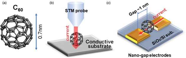
Fig. 1. (Color online) (a) Schematic diagram of fullerene (C60), which consists of 60 carbon atoms. A single C60 molecule is about 0.7 nm in diameter, and there have been discoveries of spherical fullerenes with different numbers of carbons. Encapsulated fullerenes containing metals and molecules, which are about 1 nm in diameter, have also been discovered. (b) Schematic diagram of STM applying electric current to single fullerene molecule. (c) Schematic of research device in which metal electrode with gap of about 1 nm is fabricated and fullerenes are packed into gap to investigate their properties.
Download figure:
Standard image High-resolution imageIn an attempt to utilize the electronic properties of fullerenes, resistive switching behavior has been examined by placing a fullerene at the tip of a scanning tunneling microscope (STM) needle [Fig. 1(b)]. 3) In addition to its use as a tool for the local analysis of electric properties, the STM has been used as a nano-manipulator to evaluate local coupling properties to modify devices. 4–9) In ultrahigh vacuum and at cryogenic temperatures, when a bias voltage is applied from an STM tip to a single C60 molecule in a C60-deposited thin film, a local current is generated between the two C60 molecules, resulting in the formation of a dimer with a linkage bond. The dimer formation reduces the physical distance between the C60 molecules. Furthermore, current induces further extension of the linkage to form a polymer of C60 molecules. Interestingly, when the applied energy is greater than the bond formation energy, such as when a large bias voltage is applied through the STM, local bonds are reconnected, 5,6,9) and the dimer reverts to individual C60 molecules. 9,10) The changes in charge transport properties due to the polymerization of C60 molecules can be explained by first-principles calculations 11,12) and density functional theory calculations. 13) The negative differential resistance (NDR) effect of two C60 molecules was also observed by STM measurement, 14) and the conduction properties of fullerenes trapped between electrodes have also been reported for nanogap electrodes with a gap of about 1 nm. However, the purpose of using both an STM and nanogap electrodes is to demonstrate the basic functions of nanosized storage media, 5) and there is no indication of the operation as a fixed-electrode device with source and drain electrodes [Fig. 1(c)] at room temperature in ambient air.
As described above, many interesting ideas for electronic devices utilizing the characteristic properties of C60 in an STM have been reported. However, the diameter of fullerenes is less than 1 nm, which makes it difficult to fabricate them into electronic devices, even though they can be used in an STM. Nevertheless, using microfabrication techniques, fullerenes can be packed between electrodes to measure electrical conduction. 15–20) Although fullerenes are an effective means of studying electrical conduction in a single fullerene or a small number of fullerenes, even with the latest processing techniques, it is difficult to make connections with fullerenes with high reproducibility, and only a few verification devices have been fabricated. In other words, to realize devices using fullerenes, nano-implementation from a new perspective is essential, i.e. innovations in structural architecture, including electrodes, are required.
In this progress review, after introducing solution-based fullerene nanowires (NWs) synthesis with some suggested possible applications, our new challenge of two-terminal device using self-assembled fullerene nanowires to realize a fullerene switch originally observed in an STM system on the electric device 21) is described. Particularly, experimental details are intentionally expressed for experimental reproducibility. This is because, although a two-terminal device consisting of source and drain electrodes is expected to be applied to resistance-switching applications, 22) the as-grown C60 NWs had low conductivity and more than 99% of the C60 NW devices are insulators. To solve this issue, we needed to modify the C60-C60 coupling formed in the polymerization of fullerenes. It has been pointed out that the conductivity of C60 NWs can be controlled by adjusting the dose of the irradiated electron beam (EB), and we used this method to adjust the NW conductivity. Upon the application of an EB with a moderate dose, the current–voltage (I–V) characteristics of the C60 NWs showed a nonlinear increase in the high-voltage region, indicating that additional dimerization was stimulated along the current path. When the current in the NWs reached a critical value (typically 100 μA), the I–V characteristic showed reproducible NDR. Furthermore, when the bias voltage was varied, two-state resistive switching was observed. These phenomena suggest that the conductivity of C60 NWs can be switched by an external input, which is due to the polymerization and depolymerization of the C60 polymer network in the NWs. 21) The above observation of NDR and two-state resistive switching in the fullerene crystal nanowire was the firstly reported. Then, for generally reproducing the first switching operation, details of specimen fabrication and measurement scheme with the step-by-step electric measurement in the two-terminal C60 NWs were described as a progress review.
2. Experimental methods
Although it is extremely time-consuming to directly mount a single C60 molecule with a diameter of 0.7 nm on an electronic device by itself, it becomes much easier to handle C60 molecules crystallized to a micrometer crystal. The growth of a C60 NW crystal has been established by Miyazawa, who synthesized C60 NWs by the liquid–liquid interfacial precipitation (LLIP) method. 23,24) The mutual diffusion of good and poor solvents maintains a supersaturated solution of C60 and promotes the self-assembled growth of C60 NWs. In this synthesis, C60 powder was prepared in a glass bottle and dissolved in 40 mg toluene (a good solvent) to make a saturated solution [Figs. 2(a)-i and 2(a)-ii]. C60 NWs grow at the liquid–liquid interface and precipitate when they become large. The typical diameters of C60 NWs were of the 10 nm to μm order, and the typical lengths were of the μm to 100 μm order. The diameter and length of the C60 NWs can be tuned to some extent by adjusting the reaction time, temperature, light irradiation, solvent type, solvent ratio, and the area of the liquid–liquid interface. 23–29) The diameter distribution of the C60 NWs used in the switching device study was 710 ± 470 nm [scanning electron microscopy (SEM) image: Fig. 2(b)]. C60 NWs prepared from toluene solution have an hcp structure immediately after synthesis, which changes to an fcc structure when solvent molecules are removed by drying. 30–33)

Fig. 2. (Color online) (a) Schematic of synthesis procedure for C60 crystal NWs. (b) SEM image of C60 NW aggregate removed from solvent. Adapted with permission from Ref. 21. Copyright 2021. American Chemical Society.
Download figure:
Standard image High-resolution imageIn general, an electric conduction of the C60 NWs has been pointed out as n-type semiconductor or metallic conductor. Overlook of electrical characteristics related to the LLIP synthesis is detailed in Ref. 23. The carrier mobility of C60 NWs has been reported to be in the range of 0.020–11 cm2 V−1 s−1 34–36) and strongly depends on the crystal domain size in the C60 NWs, the impurity density, and the lattice order of C60. The diameter dependence has been considered as surface oxidation and/or crystal morphology change. The C60 NWs were examined for some applications, including field effect transistors (FETs), 34) solar cells, 37,38) photo-catalysts, 39) chemical-sensors, 40) and photo-sensors. 41) Furthermore, alkali metals doping realized superconducting property 23,42–44) although the values of the superconducting transition temperature Tc were slightly lower than a conventional bulk composition of K3.3C60. Further new type NW cocrystals composed of fullerene and porphyrin, which were also synthesized by LLIP method, have been recently reported. 45–47) The NW cocrystal behaved as a channel of ambipolar field-effect transistor 45) and showed near-infrared light-sensing property. 46,47) The NWs' properties of these applications have been discussed as important electric elements for lightweight and flexible devices for future energy-saving equipment.
In addition, the conductivity of the C60 crystals can be affected by light irradiation 48–52) and EB irradiation. 53–57) For example, after prolonged exposure to UV–vis radiation, the C60 film transforms into a two-dimensional hexagonal photopolymer exhibiting semiconducting behavior, 58) and EB irradiation 59) transforms the C60 molecules into a peanut shell structure exhibiting metallic conduction. 58) Even during the observation of C60 NWs using our 200 keV transmission electron microscopy (TEM) device (JEOL JEM-2100Plus), we were able to catch a glimpse of the change in NW structure due to EB irradiation, and the contrast of the fine structure changed after a long continuous observation. The EB dose for this TEM observation was estimated to be between 65 and 260 Ccm−2. In addition, it was found by Raman spectroscopic characterization that an EB dose of 67 Ccm−2 is required to transform the C60 cage structure into amorphous carbon (under a 200 kV acceleration voltage). 60)
To evaluate the electrical conduction properties of C60 NW, C60 NW devices were fabricated on a SiO2 (250 nm)/Si substrate (Fig. 3). First, C60 NWs dispersed in isopropyl alcohol (IPA) were dispersed on the substrate, and multiple tungsten (W) wires were placed in a grid [Fig. 3(b)] for use as a deposition shadow mask, Au was vacuum-deposited under a pressure of less than 40 × 10–4 Pa to form a thin film with a thickness of about 600 nm. After deposition, the W wires were removed and observed under an optical microscope to identify the area where the C60 NW bridges the adjacent Au electrode. This is because the C60 NWs were irregularly dispersed. Instead of W wires, a metal shadow mask can also be used for metallic contact formation (Fig. 4). In this case, although a sample can be rapidly prepared for experiments, the length between the two contact pads is one order larger than that when using a W wire mask (Fig. 5). The advantage of this method is not only that electrodes can be easily formed on the wires, but also that the organic resist and EB irradiation processes can be removed to make the device. No chemical penetration or EB effect change occurs during the device fabrication process for fundamental characterization.
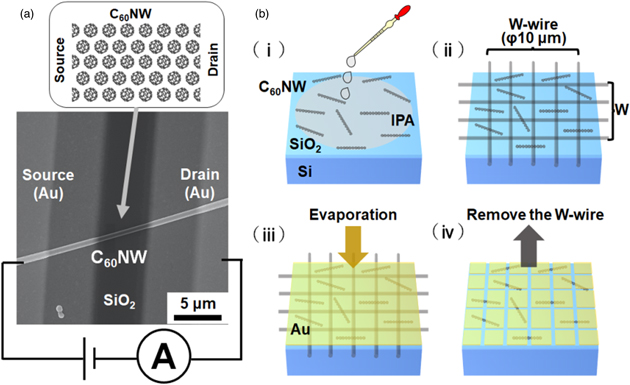
Fig. 3. (Color online) (a) SEM image of C60 NW bridged between source and drain electrodes. (b) Schematic of fabrication procedure for C60 NW device. (i) IPA solution containing C60 NW added dropwise to SiO2/Si substrate. (ii) W wires placed as shadow mask. (iii) Au film with thickness of 600 nm formed by vacuum deposition. (iv) Mask removed and cross-linking point of C60 NW identified. Adapted with permission from Ref. 21 Copyright 2021. American Chemical Society.
Download figure:
Standard image High-resolution image
Fig. 4. (Color online) (a) Optical microscopy image of stainless plate shadow mask. Regular squares are placed on the metal plate. (b) Preparation for metal electrode evaporation on NW. Because of the limitations of mask fabrication, 50 μm is the shortest distance between the pads.
Download figure:
Standard image High-resolution image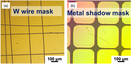
Fig. 5. (Color online) Optical microscopy images of fullerene NWs with Au electrodes. (a) W wire mask and (b) stainless plate mask. The typical length between the contact pads is determined to be of the μm order for a W wire mask and 50 μm for a stainless plate mask.
Download figure:
Standard image High-resolution image3. Results on EB Preset and I–V Characteristics of C60 NW
The electrical characteristics of the C60 NW devices were investigated in vacuum (less than 1.0 × 10⁻² Pa) in the dark at room temperature. The two-terminal I–V characteristics of the newly grown C60 NWs show that only a low current of nA order flows when a voltage of 20 V is applied between the source and drain electrodes [black dotted line in Fig. 6(a)]. The low current was mainly caused by hopping conduction. 61)

Fig. 6. (Color online) (a) I–V characteristics of C60 NW before and after EB irradiation. The inset shows the I–V characteristics of the low-voltage section. (b) I–V characteristics when transitioning from high-resistance to low resistance (set). (c) I–V characteristics when transitioning from low resistance to high-resistance (reset). Adapted with permission from Ref. 21. Copyright 2021. American Chemical Society.
Download figure:
Standard image High-resolution imageAfter our structural observation of the NW by SEM, the effect of increasing the current was observed in the I–V characteristics (Fig. 7). A short SEM observation using a 50 keV EB increased the NW current according to the I–V characteristics [Fig. 7(a)]. Then, we intentionally exposed the C60 NW to long-time EB irradiation [Fig. 7(a): 60 min exposure to 300 pA EB]. There was no obvious difference observed in the SEM images captured before and after EB irradiation [Fig. 7(b)]. Therefore, the SEM scan mode of an EB lithography system (Elionix ELS-7500), which has a stable beam current variation of less than 1% over several hours, was used to measure the current flow in the C60 NWs. The C60 NWs were continuously irradiated with an EB while a high vacuum of more than 1.0 × 10⁻⁴ Pa was maintained in the lithography system to prevent hydrocarbon contamination. The irradiation was carried out for 6.0 h using a beam current of 600 pA at an acceleration voltage of 50 kV. The total electron dose was 24 Ccm−2. On the basis of the results of previous studies, 60,62) the electron dose used in this experiment was sufficiently smaller than that required to induce a conformational change in the C60 molecules. As a reference, from a comparison with the results of a previous study based on the McKinley–Feshbach equation 63) using graphite, 60) it was inferred that the irradiation conditions in our EB lithography did not lead to irreversible deformation of the C60 cage.
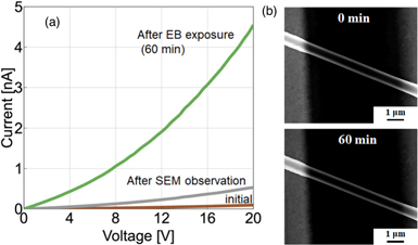
Fig. 7. (Color online) (a) I–V characteristics of initial NW, NW after short SEM observation, and NW after 60 min EB exposure. (b) SEM images of NW before and after 60 min EB exposure. No change was observed.
Download figure:
Standard image High-resolution imageAfter the EB irradiation, the current in the C60 NW increased significantly, reaching about 120 times than that before irradiation [Fig. 6(a)]. The current in the C60 NW depended on the cumulative EB irradiation, which depended on the EB dose (Fig. 8). EB irradiation generates C60-C60 linkages (=dimerization) in the C60 NW. Further EB irradiation induces C60 polymerization with long polymers. These long polymers increased the current in the I–V curve.

Fig. 8. (Color online) Dependence of source–drain current on irradiation dose density. For current measurement, 20 V was applied. The dotted line, calculated from the current near the conductive region by the least-squares method, is a guide to the eyes.
Download figure:
Standard image High-resolution imageAfter EB irradiation, the device showed clear ohmic I–V behavior even at a low bias voltage [Fig. 7(a) inset]. When the voltage was further increased in this device, the current increased nonlinearly in the corresponding I–V curve [Fig. 6(a)]. This nonlinear increase allows a higher density of current to flow through the C60 NW, and the flowing current stimulates additional polymerization near the conduction path to expand the polymerized segment. When the voltage was further increased, the current increased sharply at 38 V, as shown in Fig. 6(b). This sudden increase was caused by the sudden direct connection of the conduction path from the source electrode to the drain electrode by the polymerization of C60 molecules. As a result, the current flow was markedly improved and the fullerenes became more connected. However, further increase in voltage caused the pathway to break, resulting in a decrease in current (the mechanism of this breakage is discussed below). This decrease is regarded as NDR. The NDR voltage was 10 V, which was observed reproducibly in repeated I–V measurements. A SEM image with 16 000-fold magnification showed no change in the C60 NWs after the occurrence of NDR, indicating that the current drop was not caused by the structural breakdown or channel burning by a high density current flow. On the other hand, low-conductivity C60 NWs with insufficient EB irradiation did not exhibit NDR even when a bias voltage of 100 V was applied, indicating that sufficient current due to C60-C60 polymerization is essential for observing NDR, and the increased current leads to a nonlinear increase in current that causes NDR (i.e. preset conduction path). Note that when NDR occurs and the state shifts to a high-resistance state (HRS), a sudden drop in current occurs and a small current remains. Provided this NDR in the HRS does not burn out the C60 NW, NDR can be observed repeatedly in I–V measurements. However, once an extremely large voltage is applied, the high-resistance channel carrying this small current disappears. The structural breakage of C60 NWs is often observed in electrostatic destruction.
4. Results on C60 NW resistance-switching properties
The two-terminal C60 NW device with NDR has two bistable resistance states: a low-resistance state (LRS) and an HRS. These bistable states can be reversibly reproduced by applying an external voltage (Fig. 9). When the external voltage is applied to each of these bistable states, a continuous switching of the resistance can be achieved as shown in Fig. 9. The voltage sequence for the switching operation consists of three different voltages: "set," "reset," and "lead" [Fig. 9(a)]. The set voltage is determined from the peak voltage of NDR. For example, in Fig. 6(c), it is 11 V and the reset voltage is 14 V. The readout voltage was set to a small value such as 0.2 V so that the readout would not cause any change in conductivity. To avoid damage due to overcurrent at the set voltage, the circuit compliance was set to 60 μA in the measurement program.
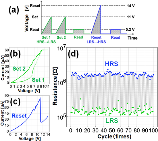
Fig. 9. (Color online) (a) Sequence of voltage cycles for resistive switch test: "set," "reset," and "read." (b) I–V characteristics during set (HRS → LRS) operation: a compliance of 60 μA is set, and voltage is applied twice, shown as Set 1 and Set 2. (c) I–V characteristics during reset (LRS → HRS) operation. (d) Resistance transition during 100 switch cycles at room temperature. Adapted with permission from Ref. 21 Copyright 2021. American Chemical Society.
Download figure:
Standard image High-resolution imageWhen the set voltage was applied, the conductivity of the C60 NW increases and the NW enters an LRS [Fig. 9(b)]. Here, it is noted that the LRS resistance can be measured at the reading voltage, but it is not the lowest resistance from the NDR peak value. In this measurement, a double set voltage scheme was applied to obtain a clear LRS. This is because a single set voltage could also induce the LRS, but set errors with intermediate resistance values occurred frequently.
When the reset voltage is applied, the conductivity decreases and the C60 NW maintains an HRS [Fig. 9(c)]. The resistance of the C60 NW after the reset voltage, i.e. after entering the HRS, was also measured at the readout voltage (0.2 V) and is plotted in Fig. 9(d). The LRS and HRS are repeatedly induced by alternating the set and reset voltages. Even after 100 repetitions of switching, the LRS and HRS are distinct, and the LRS/HRS current ratio is 10. Compared with a metal resistance change element, the C60 NW shows high reproducibility in its switching behavior. To the best of our knowledge, the resistive switch observed in fullerene nanowires has not been reported before, and we would like to emphasize that this is the first result obtained in fullerene nanowire, and a significant progress as room temperature operation.
Figure 10 shows the results of 300 repetitions of switching, indicating clear variations in the current values of the LRS and HRS. Such variations can be reduced by adjusting the operating voltage and improving the C60 NW. Specifically, the multiple parallel and series resistors in the C60 NW are considered to affect the current and the current modulation in the switching operation, and there is room for improvement by optimizing the device structure and the diameter and length of the C60 NW. However, we emphasize that, to the best of our knowledge, the achievement of 300 cycles at room temperature is the most stable operation reported for polymer-based memories.
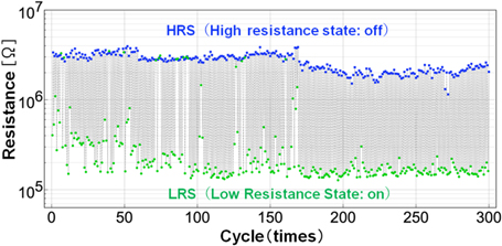
Fig. 10. (Color online) 300-cycle continuous switching operation of C60 NW device at room temperature.
Download figure:
Standard image High-resolution image5. Discussion
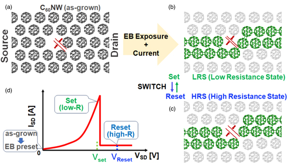
The reproducible switching properties of C60 NWs can be explained by polymerization and depolymerization along the main conduction path (Fig. 11). The model of the conduction path can be switched between polymerization and depolymerization for the electrical LRS and HRS as shown in Fig. 11.
Fig. 11. (Color online) Model diagram of NDR and switching phenomenon of C60 NW: (a) crystal NW just after preparation, (b) C60 NW in LRS with connection made by polymerization, (c) C60 NW in HRS with disconnected polymerization segment, and (d) set and reset voltages in I–V diagram. Adapted with permission from Ref. 21 .Copyright 2021. American Chemical Society.
Download figure:
Standard image High-resolution image
After EB irradiation, some C60 molecules polymerize into dimers and even polymers in the C60 NW between the source and drain electrodes, and the two-terminal resistance decreases. After EB irradiation, some of the C60 molecules polymerize into dimers and then into polymers in the NW between the source and drain electrodes, and the two-terminal resistance decreases [Fig. 11(b)]. When the voltage is further increased, a large current is generated, and the current flows in the main conduction channel, generating heat, and the polymerization proceeds rapidly, which is observed as a nonlinear increase in the current [Fig. 11(d)].
On the other hand, when the C60-C60 linkage occurs, the physical distance between C60 molecules shrinks. This shrinkage results in the loss of polymer continuity, causing a reduction in electrical conduction due to the extra spaces between adjacent C60 polymers. The thermal effect that potentially generates the nonlinear current increases. The thermal dissociation of dimer bonds has been reported to occur in a process that exhibits Arrhenius-like behavior with an activation energy of 1.25 eV. 10,64) The conversion to bond dissociation occurs at a temperature above 100 °C. 5,64) This heating effect is also responsible for the breaking of conduction paths. This heat also contributes to the chain reaction of conduction path breaking, resulting in a decrease in current. Since the polymerization and depolymerization of C60 are basically reversible changes in C60, current will flow again if the previous set voltage is applied.
The above depolymerization due to excess current is most likely to occur at the weakest polymer connection. This process forms a bistable C60 connection at the C60–polymer segment junction end for the NDR appearance. When the dominant conduction pathway is disconnected, the resistance increases in the HRS [Fig. 11(c)]. When a moderate current is applied with a set voltage to promote bond connection, the current path is re-established for the LRS. Owing to the shortened distance between the C60 molecules during tuning, the most likely situation is that the application of the set and reset voltages will result in a slight shift in the position of C60, which is the dominant process by which the polymers are connected. From this consideration, it can be inferred that the stability of the measurable resistance in the HRS and LRS is dependent on the distance of the shift. The variations in the LRS and HRS shown in Fig. 10 may be related to statistical fluctuations with respect to the inter-C60 bonding chemistry, which will be pursued in the future. The variations in the LRS and HRS values are due not only to the contact resistance of the C60 NW two-terminal device, but also to the resistance caused by the multiple parallel and series polymers in the NW. In the future, we would like to optimize the conduction path by modifying the device structure. In addition, we will try to improve the method of fabricating the device so that the total size of the device will be close to that of a single fullerene molecule.
6. Conclusions
In this progress review of our challenging device, we have presented details of fabrication of the C60 NW resistance switching device with electrical switching operation, which was caused by C60 polymerization and depolymerization in a self-assembled fullerene NW. 21) The C60 NW was synthesized at a liquid–liquid interface and was electrically characterized in a two-terminal contact configuration at room temperature. In the two-terminal measurement, once NDR occurred, a two-state resistive switch was repeatedly observed upon applying an input voltage. The mechanism of the two-state resistive switch was based on the basis of controlling the polymerization and depolymerization of C60 to connect/disconnect the polymerized C60 segment boundary in the NW. The polymerization was stimulated by the induced current, while the depolymerization was caused by the thermal decomposition of chemical bonds due to the thermal activation.
We expect that our results will provide a new mechanism for sub-nanometer device switches. 21,65) Such ultrasmall switches are expected not only to contribute to the miniaturization of switch and memory assemblies, but also to achieve extreme energy conservation owing to the need to adjust only one bond for switching to occur.
Acknowledgments
This work was supported by JSPS Grant-in-Aid for Scientific Research 20K05291. We would like to express our sincere gratitude to Dr. Shushu Zheng (WPI-MANA, now Zeiss) for his helpful advice on sample preparation, Mr. Mihiro Takeuchi (Chiba Institute of Technology) and Mr. Hiroyuki Motoyama (Chiba Institute of Technology) for their cooperation in sample preparation, and Dr. Tomonobu Nakayama (WPI-MANA, NIMS), Prof. Katsunori Wakabayashi (Kwansei Gakuin University), Dr. Takatsugu Wakahara (NIMS), Dr. Yasuhisa Naito (AIST), and Dr. Akichika Kumatani (Tohoku University) for their helpful advice in interpreting the observed results.
Biographies

Kazuhito Tsukagoshi studied experimental research on transport physics in semiconductor microstructures and completed his PhD. (Osaka University) in 1995. After that he worked as a visiting associate in Cavendish Laboratory (University of Cambridge, U.K.) and then in Hitachi Cambridge Laboratory (Hitachi Europe Ltd., U.K.). In 1999, he joined RIKEN, where he carried out research on functional thin-film electronics. He continued this research in AIST in 2008 and moved to NIMS in 2009. His current research focuses on nanomaterial applications for nanoelectronics.

Yukiya Umeta studied experimental research on nanomaterials for nanoelectronics and completed his master's degree (Chiba Institute of Technology) in 2021. After that he joined ABLIC Inc.

Hiroshi Suga studied experimental research on electron transport in nanostructures and completed his PhD. (Nihon University) in 2008. After that he worked as a postdoctoral researcher in AIST. In 2012, he joined Chiba Institute of Technology where he carried out research on functional nanostructures. His current research focuses on nanomaterial and nanostructure applications for nanoelectronics.