
Abstract
This paper reviews the 35 years of history of plasma-excited MBE, focusing on the special value added to conventional MBE through the usage of plasma-excited molecular beams. These advantages include low-temperature surface cleaning, low-temperature growth, selective-area regrowth and impurity doping. These technologies are extremely important to realizing nanoscale low-dimensional device structures. True band gap of InN was identified only after high-quality InN became available by using plasma-excited MBE. Future prospects of this technology are also included from the device application viewpoint.
Export citation and abstract BibTeX RIS
1. Proposal of ECR–MBE
In the 1980s, optical and electronic devices based on GaAs, InP and related alloys were extensively studied for use in next-generation microwave and optical communication networks. Devices with quantum wells and superlattices attracted much attention. Two-dimensional electron gas formed at sharp and flat hetero-interfaces also attracted much attention for high-frequency and high-speed electronic devices. To fabricate these nanostructures, new technologies like metal-organic CVD (MOCVD) and MBE were intensely studied replacing the conventional liquid-phase epitaxy (LPE) and vapor-phase epitaxy technologies as growth methods. Among these technologies, MBE has strong advantages in obtaining flat, sharp and thickness-controlled films and hetero-interfaces in the atomic level.
For further development of advanced devices, quantum effect devices with quantum wires and quantum dots have attracted further attention. To fabricate these sophisticated structures in the nanoscale, technological developments in low-temperature and selected-area regrowth technology have become increasingly important. It is commonly understood that conventional MBE is carried out under thermal non-equilibrium conditions, which cause a lack of atom migration on the growing surfaces, resulting in poor film quality. To solve this problem, extra energy in the form of plasma, ions or light is required on the growing surfaces, especially when growth is carried out at low temperatures.
ECR plasma, excited by a 2.45 GHz microwave with a 0.0875 T divergent magnetic field, is a very effective plasma source, which can generate and maintain plasma even in 10–5–10–4 Torr vacuum. This plasma source can transport high-density and low-energy ions (20–30 eV) very effectively onto the substrate by a divergent magnetic field. This ECR plasma source has been widely applied to low-temperature deposition of insulating dielectric materials like SiN and SiO2, 1) dry etching 2,3) and high-speed sputtering 4,5) processes.
We have proposed an ECR–MBE growth method, connecting an ECR plasma source and an MBE growth system. 6) A home-made ECR–MBE growth system was developed at NTT Research Laboratory in 1987. A schematic diagram of this ECR–MBE system is shown in Fig. 1. 7)
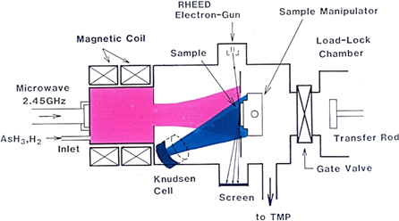
Fig. 1. (Color online) Schematic diagram of the ECR–MBE system, which consists of an ECR plasma source, an MBE chamber and a load-lock chamber for sample transfer (reproduced from Ref. 7).
Download figure:
Standard image High-resolution image2. Low-temperature growth of GaAs
A noticeable advantage in reducing temperature for substrate cleaning and consequent growth was experimentally proved as soon as ECR–MBE growth was applied for the preparation of GaAs films on GaAs substrates. Reflection high-energy electron diffraction (RHEED) patterns before and after H2 plasma cleaning and those after MBE growth at temperatures between 300 and 550 °C are compared in Fig. 2. 7)
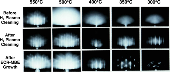
Fig. 2. (Color online) RHEED patterns from GaAs at each temperature. Upper row, before H2 plasma cleaning; middle row, after H2 plasma cleaning; and bottom row, after GaAs growth at each temperature by ECR–MBE (reproduced from Ref. 7).
Download figure:
Standard image High-resolution imageSubstrate surfaces after thermal cleaning at various temperatures less than 400 °C show a diffuse pattern indicating the existence of oxides. A streak pattern appears only after reaching 550 °C. In contrast, streak and reconstructed patterns can be observed after H2 plasma cleaning even at temperatures as low as 300 °C, indicating the pronounced advantage of removing oxides from the surface by H2 plasma at low temperature. The bottom row in Fig. 2 shows the RHEED patterns after growth of GaAs on top of GaAs substrate surfaces treated by H2 plasma, which demonstrate that single-crystal GaAs film can be grown epitaxially even at temperatures as low as 350 °C.
Surface cleaning of Si substrates by H2 plasma and subsequent low-temperature growth of GaAs has also been carried out. A (2 × 2) reconstructed pattern of the Si surface has been successfully obtained after H2 plasma cleaning even at 400 °C, 8) which is much lower than 1000 °C. It is well known that at least 1000 °C is required for Si surface cleaning by conventional thermal methods. GaAs growth at 400 °C on the plasma-treated Si substrate has been carried out. A clean interface between GaAs and Si has been successfully obtained. No obvious impurity pile-ups of oxygen and carbon at the growth interface have been observed by secondary-ion mass spectrometry (SIMS) analysis. 8)
3. Selective-area growth of GaAs
Selective-area growth of GaAs by conventional MBE is usually unsuccessful, resulting in the deposition of polycrystalline GaAs islands on top of the dielectric mask materials, like SiN and SiO2. With a supply of proper plasma power and with proper negative bias to the substrate, successful selective-area growth of GaAs can be achieved at 630 °C only on the opening area of GaAs formed by a 1 μm/1 μm SiN mask patterned to the [011] direction. Selectively grown GaAs has both (001) and ( ) facets as shown in Fig. 3.
9) It has been found that an increase in excitation power and negative bias, which accelerate positively charged Ga ions to reach the substrate, improves selectivity as shown in Figs. 4 and 5.
10)
) facets as shown in Fig. 3.
9) It has been found that an increase in excitation power and negative bias, which accelerate positively charged Ga ions to reach the substrate, improves selectivity as shown in Figs. 4 and 5.
10)
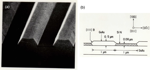
Fig. 3. (Color online) (a) SEM bird's-eye view image of selective-area growth of GaAs. (b) Schematic diagram of the cross-sectional structure. (Reproduced from Ref. 9.)
Download figure:
Standard image High-resolution image
Fig. 4. (Color online) Selectivity dependence on microwave power for (a) 30 W, (b) 100 W and (c) 300 W. Cross-sectional view (d), which shows where each of the images is taken. (Reproduced from Ref. 10.)
Download figure:
Standard image High-resolution image
Fig. 5. (Color online) Selectivity dependence on bias voltage to the substrate for (a) +20 V, (b) 0 V and (c) −20 V (reproduced from Ref. 10).
Download figure:
Standard image High-resolution imageEven when the mask width changes with the GaAs opening width kept constant, the thickness of the GaAs selectively grown in this opening area is kept constant and does not change. 9,10) This result is a clear contrast to the MOCVD case. In the case of selective-area growth by MOCVD, the thickness of GaAs in this opening area increases as the mask width increases. This is due to Ga migrations from the mask surface to GaAs in the opening area, which can successfully explain the selective-area growth mechanism by MOCVD. The selective-area growth mechanism in ECR–MBE, on the other hand, should be explained by the re-evaporation of Ga from the mask area before it reaches the opening area by atom migration. 9)
4. Role of radicals and ions in ECR–MBE
It was reported that surface cleaning by He plasma is found to be not as effective as that by H2 plasma. 8) On the other hand, cleaning by H2 plasma with +50 V bias is as effective as that with no bias. When we apply +50 V bias to the substrate, most of the positive ions from this ECR plasma source with a divergent magnetic field can be considered to be repulsed and not reach the substrate surface. 11) Accordingly, it is reasonable to consider that H radicals should play a major role in the surface cleaning process at low temperature. On the other hand, positive ions generated in ECR plasma are considered to have a major role in achieving selective-area growth when clear selectivity dependence on microwave power and negative bias conditions 4,5) is taken into account.
GaAs subjected to ECR plasma is etched or sputtered and reduces its thickness. Figure 6 shows how the thickness of GaAs grown by ECR–MBE is reduced depending on the microwave input power to the ECR plasma source. 7) Pronounced reduction of grown layer thickness is observed even after adjusting the amount of solid GaAs film etched in the plasma process. This reduction apparently comes from the enhanced desorption of physically adsorbed and migrating Ga before completing chemical bonding at the kink or step site of the GaAs surface.
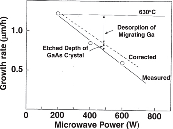
Fig. 6. (Color online) Growth rate dependence of GaAs on microwave power. The horizontal dashed line shows the expected growth rate from the supplied Ga to the substrate. The solid line shows the experimentally achieved actual growth rate dependence on input microwave power. The diagonal dashed line shows the corrected growth rate dependence on input microwave power after adjustment of the GaAs etched thickness in plasma for each microwave power. (Reproduced from Ref. 7.)
Download figure:
Standard image High-resolution imageAccordingly, the selective-area growth mechanism of GaAs with a SiN mask, mentioned previously, can be explained by the enhanced desorption of migrating Ga on the SiN mask, due to impinging positive ions, whereas most of the Ga supplied on the GaAs opening area can reach the kink or step site of the GaAs surface and complete stable chemical bonding. This mechanism can successfully explain the independence of selectively grown GaAs thickness from mask width. 9,10)
Thus, it is found that radicals generated in H2 plasma have a major role in cleaning the GaAs surface at low temperature, whereas positive ions generated in plasma have a major role in realizing selective-area growth of GaAs by ECR–MBE.
5. GaAs regrowth on processed AlGaAs
Regrowth technology of GaAs quantum dot or quantum wire structures on processed AlGaAs is essential to fabricating GaAs quantum structures surrounded by wider band gap AlGaAs. Here, formation of oxides on the AlGaAs surface after the chemical process is crucial, as oxides formed on AlGaAs during or after chemical processes cannot be removed only by a thermal process. This causes the formation of even more stable Al2O3 after high-temperature annealing in vacuum.
ECR–MBE is found to be very effective in solving this critical issue, making it possible to form GaAs nanostructures embedded in AlGaAs. SIMS depth profiles of GaAs films grown on AlGaAs substrates prepared by various cleaning conditions and corresponding AlGaAs RHEED patterns are compared in Fig. 7. 12) Oxygen and carbon pile-ups at the growth interface are significantly reduced as compared with the thermal cleaning case and totally removed by lowering the temperature for plasma cleaning. This suggests that oxygen impurity removal by H2 plasma is essential before stable Al2O3 formation by thermal treatment.
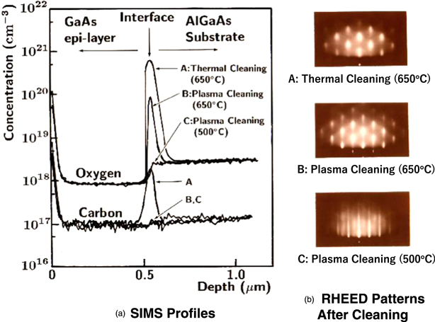
Fig. 7. (Color online) (a) Depth profiles of oxygen and carbon determined by SIMS for (A) GaAs grown on thermally annealed AlGaAs at 650 °C, (B) GaAs grown on hydrogen plasma cleaned AlGaAs at 650 °C, and (C) GaAs grown on hydrogen plasma cleaned AlGaAs at 500 °C. (b) Corresponding RHEED patterns on AlGaAs after each cleaning process. (Reproduced from Ref. 12.)
Download figure:
Standard image High-resolution imageDirect growth of AlGaAs/GaAs single quantum wells (SQWs) on GaAs substrates cleaned by ECR H2 plasma has been carried out without inserting buffer layers. SQW structures were successfully grown by ECR–MBE after the cleaning process without breaking the vacuum. Results of photoluminescence (PL) and atomic force microscopy (AFM) measurements have shown high structural and optical quality of the SQWs. 13) This proves the effectiveness of the H2 plasma process by ECR–MBE as a regrowth technology.
ECR–MBE technology with low-temperature cleaning and growth capability together with selective-area growth capability has proved to be a powerful potential method to fabricate low-dimensional GaAs nanostructures in wider band gap AlGaAs with atomic-scale structural control. This technology has also been demonstrated to be a potential candidate as a method to form GaAs nanostructures on Si at low temperature where thermal mismatch is pointed out as a big concern. 14)
6. GaN growth by ECR–MBE
GaN growth is commonly carried out by MOCVD at around 1100 °C or higher. MBE has also attracted attention as a growth method for GaN and related alloys with thickness control in the atomic layer level with sharp and flat hetero-interfaces. N2 gas and NH3 are the two major candidates for group V sources. Higher temperature is required in the case of NH3-source MBE for NH3 decomposition. The high chemical reactivity of NH3 with vacuum chambers and other growth equipment also introduces additional difficulty. On the other hand, due to the stability of N2 gas, it is not easy to use it as a group V source as long as standard gas source MBE is considered. ECR–MBE has already been proved to be a powerful tool for a low-temperature growth method from our previous studies on GaAs.
We started to grow GaN by ECR–MBE in the middle of the 1990s. Here, low-temperature growth capability was effectively utilized for GaN growth and high-quality polycrystalline GaN growth was successfully carried out even on silica glass at 700 °C. Surprisingly, the PL intensity from this GaN was even stronger than that from single-crystal GaN film grown on sapphire substrates. 15) This result has attracted much attention as a growth method for nitride-based display devices on silica glass.
GaN growth studies on sapphire substrates have demonstrated the importance of the nitridation process of sapphire substrates prior to growth to obtain high-quality GaN films. Here, an ECR plasma source with a high density of ions with controlled energy has obvious advantages in lowering temperatures and reducing the time of nitridation of sapphire.
At the beginning, GaN grown by MBE, however, had generally poorer quality than MOCVD-grown GaN on sapphire substrates. A two-step growth method with low-temperature nucleation growth and subsequent high-temperature GaN growth is generally employed for MOCVD growth. A similar two-step growth process was also found effective for MBE growth and is employed widely. It is well known that a low-temperature-grown GaN nucleation layer on a nitridated sapphire substrate includes both Ga-polar and N-polar GaN. During the following high-temperature growth, this polarity is preferentially selected and dominated by Ga-polar GaN in the case of MOCVD, due to its high temperature. In contrast, GaN grown by MBE generally contains a high density of mixed-polarity domains due to shortage of energy to flip over the polarity of GaN. This crucial polarity control problem of GaN MBE growth on sapphire was gradually solved after employment of GaN templates, which were prepared by MOCVD on sapphire substrates prior to MBE growth. Thus, the application of templates made it possible to grow GaN film with the same level of quality as that grown purely by MOCVD.
Optical emission spectroscopy (OES) 16) has been used as a monitoring tool in ECR–MBE growth of GaN, as ECR plasma is an effective source for producing not only low-energy ions but also highly excited neutral molecules and atoms even in high-vacuum conditions. ECR–MBE has been successfully applied to low-temperature growth of GaAs and GaN, as shown previously. Since nitrogen plasma includes various excited species such as excited molecular (N2 *), molecular ionic (N2 +), atomic (N*) and atomic ionic (N+) nitrogen, identification of excited species near the substrate is very important not only to understand the growth mechanisms of ECR–MBE in the atomic scale but also to obtain high-quality epitaxial films.
It has been well known that GaN generally crystallizes in stable hexagonal structures but also in metastable cubic structures. Selection of these phases can be controlled by adjusting the substrate symmetry. Cubic GaN can be grown on substrates with cubic symmetry like (001) GaAs or 3C-SiC. From our previous studies, we have also found that both symmetries can be well controlled by changing the growth temperature or V/III ratio on the substrate surface. It was found for the first time that the crystal structure can be easily controlled simply by changing the bias conditions to the substrate. 17) Greater positive bias changes the GaN crystal symmetry from hexagonal to cubic phase. OES studies have identified the decrease of Ga* emission intensity, suggesting the decrease of Ga desorption from the substrates. It can be explained by the fact that positive bias to the substrate decreases the impinging energy of positive ions to the substrate. Desorption of Ga, which is physically adsorbed and migrates on the substrate, is suppressed by greater positive bias. This result suggests a new possibility of changing the effective V/III ratio on the growing surfaces electrically, rather than by employing a temperature change of the Knudsen cell. This can give us a much quicker and simpler way to change the effective V/III ratio during growth. We have proposed growth of hexagonal and cubic superlattices by simply changing the bias voltage during growth. 18)
ECR–MBE is also used for selective growth of position-controlled InN nano-columns on hole-patterned GaN templates. Results are shown in Fig. 8. 19) These nano-columns are very useful for overcoming the 11% large lattice mismatch between InN and the GaN template. Transmission electron microscopy (TEM) observation 20) has proved that InN nano-columns are epitaxially grown on GaN templates with relaxed strain. In the majority of InN nano-columns, however, neither edge-type nor screw-type threading dislocations are generated at the growth interface between the GaN template and the InN nano-columns. It is also observed that most threading dislocations from the GaN template bend against the growth direction or terminate at the interfaces, resulting in an almost dislocation-free InN in the nano-columns.

Fig. 8. (Color online) Bird's-eye view image of position-controlled InN nano-columns (reproduced from Ref. 19).
Download figure:
Standard image High-resolution image7. InN growth by RF–MBE
Among group III nitride semiconductors, InN has the narrowest band gap, lowest effective mass, highest mobility and highest saturation velocity. Due to these advantageous properties, this material has attracted much attention for application to both longer-wavelength optical devices and high-frequency, high-speed electronic devices. The difficulty in growing this material has hindered research and development of this material and related devices. This difficulty comes mainly from a low dissociation temperature and a high equilibrium nitrogen vapor pressure over InN during growth. Growth of this material by MOCVD faces an essential problem due to limitations on growth temperature. This is due to the fact that InN easily starts its thermal dissociation at the temperature required for NH3-source decomposition. As a plasma source does not have temperature limitations for N2 gas to decompose, plasma-excited MBE has an intrinsic advantage over MOCVD for the growth of InN.
In this review paper, we demonstrate the role of excited ions in enhancing the desorption of physically adsorbed Ga. This characteristic has been successfully utilized to carry out selective-area growth by ECR–MBE. The quality of material grown by ECR–MBE, however, is poorer due to damage induced by high-density impinging ions. At the same time, it has been gradually unveiled that radicals play a major role in crystal growth itself. Based on these findings, we have started to grow InN by using an RF plasma source, 21) in which plasma is generated by 13.56 MHz RF electromagnetic waves. This plasma source can supply a high density of activated nitrogen radicals without increasing the density of ions.
Selection of the growth temperature at the highest point within the InN dissociation limit was found to be essential for quality improvement. Figure 9 shows how PL intensity varies depending on the growth temperature, in which higher quality is obtained from films grown at higher growth temperatures. 22) The other essential factor for growing high-quality crystals is the selection of the optimum V/III ratio on the growing surface. This optimum condition has been intensely studied at UCSB for GaN growth. 23) They have reported that selection of growth conditions in the intermediate regime, between the Ga-rich regime and N-rich regime, is essential for growth of high-quality GaN. When films are grown under low V/III ratios with Ga-rich conditions, the surface of the film includes lots of Ga droplets. On the other hand, films grown under high V/III ratios with N-rich conditions, the quality of the layer is generally poor with a high density of pits on the film surface. Optical and electrical properties also show poor levels when films are grown with N-rich conditions.
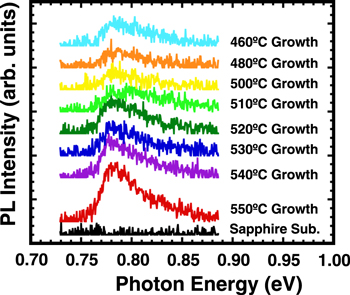
Fig. 9. (Color online) InN PL intensity dependence on growth temperature between 460 °C and 550 °C (reproduced from Ref. 22).
Download figure:
Standard image High-resolution imageIn our study on growth of high-quality InN by RF–MBE, we took the same approach to find this condition for the intermediate regime. It was found that the window for this intermediate regime is very narrow, especially for InN growth. Keeping the growth temperature, the beam equivalent pressure of In and the N2 gas flow constant at 550 °C, 3.2 × 10⁻⁷ Torr and 2.0 sccm, the effective V/III ratio on the growing surface was carefully controlled by changing the RF plasma power between 230 W and 250 W. The morphology of the grown surface showed that InN grown under 230 W grows under In-rich conditions, whereas InN grown under 250 W grows under N-rich conditions. Thus, the growth window for high-quality InN with a flat surface is found to be very narrow.
Applying all these optimum growth conditions on temperature, V/III ratio and preparation of the buffer layer, one of the highest-quality InN films at that time was obtained, 24) and high-quality InN films became available at Ritsumeikan University for detailed material characterizations.
After extensive optical and electrical property measurements using these high-quality InN films prepared by RF–MBE, surprising information on the physical properties of InN was obtained. The fundamental band gap of InN was found to be around 0.7 eV, 25) which is much less than 1.9 eV. This value had been believed to be the band gap of InN for more than 30 years. 26) This value was obtained from the optical absorption edge energy measured from polycrystal InN and InGaN prepared by sputter deposition. Energy values obtained from PL emission, optical absorption and electro-reflectance studies on our InN films all indicated simultaneously that the band gap of InN should be around 0.7 eV. 25)
This true band gap of InN can be identified only after high-quality InN became available by using plasma-excited RF–MBE. Even after this narrow band gap of InN was reported, lots of arguments have been presented over the true band gap of InN. Some argue that the band gap cannot be determined by PL and optical absorption. They claim that the origin of this luminescence or absorption could be the energy levels in the band gap induced by some kind of crystal defect. Figure 10 shows experimental evidence that measured PL peak and absorption edge energies become lower as crystal quality improves with lower X-ray rocking curve (XRC) FWHM values. 27) Figure 10 also shows that these PL and absorption edge energies decrease as the PL intensity and electrical mobility of the film increase with quality improvements. 27) These tendencies cannot be explained by defect-related emission and absorption mechanisms. In addition to the correlation between the measured band gap energy and crystallographic, optical and electrical properties, a theoretical explanation of the true band gap of InN supports a narrow band gap. 28) Here, it should be emphasized that plasma-excited RF–MBE is really responsible for the findings of this true band gap of InN.
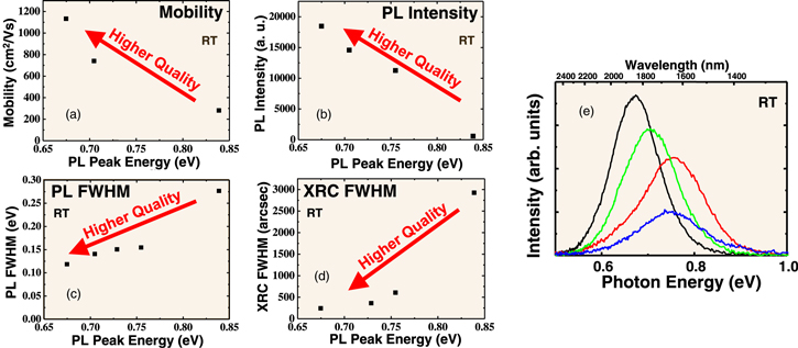
Fig. 10. (Color online) Relation between PL peak energy and (a) mobility, (b) PL intensity, (c) PL FWHM and (d) XRC FWHM. Higher-quality films show lower PL peak energy. Representative PL spectra are shown in (e). (Reproduced from Ref. 27.)
Download figure:
Standard image High-resolution imageNot only the band gap of InN, but also other fundamental physical properties of InN, like effective mass, have been revised after the re-evaluation of this material. These new findings also opened up new application fields of nitride-based semiconductors. In addition to optical devices in infrared wavelengths, application to high-frequency and high-speed electronic devices has attracted further interest due to renewed findings of much smaller effective mass and much higher expected mobility and saturation velocity. Potential application to very high efficiency solar cells over 50% has attracted even much greater attention, as it became apparent that GaN, InN and related alloys now cover almost the entire spectrum range of solar energy.
8. RF–MBE growth by droplet elimination by radical-beam irradiation
The growth window under the intermediate regime is very narrow for InN growth. Once it achieves N-rich conditions, both morphology and optical and electrical properties become poor due to lack of migration at low growth temperature. On the other hand, when it achieves In-rich conditions, In droplets start to form on the surface. This gives us a very serious problem for InN growth as these In droplets essentially cannot be removed by the thermal process.
In the case of GaN growth by MBE, one can remove these Ga droplets, formed under Ga-rich conditions, by thermal evaporation as GaN film is thermally stable at the temperature for Ga evaporation. In contrast, In droplets, formed under In-rich conditions for InN growth, cannot be thermally evaporated as thermal-equilibrium nitrogen vapor pressure over InN film is always higher than that of In evaporation from liquid In metal. This causes even larger In droplet formation on the InN film surface as nitrogen escapes faster from InN film during the thermal process for In evaporation.
As a result, more stringent control of growth conditions such as substrate temperature and the supply rates of In and nitrogen is required for InN growth compared with the GaN growth case. Keeping these optimum conditions constant all through the growth process is practically very difficult. It is widely known among scientists in this field that substrate temperature usually slightly changes as growth proceeds. Keeping plasma conditions constant is also difficult which causes fluctuation of the V/III ratio during the growth process. Once it becomes In-rich, due to fluctuation of plasma or an unexpected substrate temperature change, In droplets form on the surface, which cannot be removed by simple thermal annealing. We should solve this serious problem to make this RF–MBE technology available for practical use.
We have accidentally found that these droplets are completely removed after nitrogen radicals are supplied on the surface. During this process, the In supply is cut off by the mechanical shutter. Apparently, In droplets are transformed to a flat InN film, which should have been grown epitaxially on the substrate during the nitrogen radical supply. This unexpected result gives us a critical clue on how to grow high-quality InN epitaxial films by RF–MBE. 29)
It has been widely known that epitaxial films grown under metal-rich conditions have much higher quality in terms of both morphology and properties. We have repeated the processes of metal-rich growth and In droplet elimination by nitrogen radical beam supply several times. The films thus prepared showed much better quality than those grown by the conventional method with a simultaneous supply of In and N radicals. Flat-surface and corresponding reconstructed RHEED patterns from the grown film are shown in Fig. 11. 30)
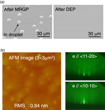
Fig. 11. (Color online) Surface morphology and RHEED patterns of InN grown by droplet elimination by radical-beam irradiation. (a) SEM surface images are compared between after a metal-rich growth process and after a droplet elimination process (DEP). (b) AFM image and corresponding RHEED patterns observed after DEP. (Reproduced from Ref. 30.)
Download figure:
Standard image High-resolution imageBased on these remarkable results, we have named this growth method droplet elimination by radical-beam irradiation (DERI). 30) This DERI process consists of a sequence of two growth steps with an In-rich growth step (MRGP: metal-rich growth process) and a subsequent N radical irradiation step (DEP: droplet elimination process). It should be emphasized that we do not need to take stringent control of the V/III ratio in a very narrow growth window. All we need is to grow InN under In-rich conditions. Later, it was found that a simple supply of several monolayers of In during MRGP before a supply of N radical beams gives us the same results.
InN films grown by this DERI method show reproducible high quality. Figure 12 compares the electrical properties of epi-films grown by the conventional and DERI methods. 31) It should be noted that the electrical properties of films grown by conventional methods scatter run to run, whereas those grown by the DERI method show reproducible high quality even when they are less than 500 nm thick. The films thicker than 500 nm showed even higher mobilities. It should be emphasized that reproducibility is essential to being a practical technology for growth of InN.

Fig. 12. (Color online) Carrier concentration and Hall mobility for InN grown by conventional method (■) and by DERI method for samples around 500 nm thick  and thicker than 500 nm
  (reproduced from Ref. 31).
Download figure:
Standard image High-resolution image9. In situ observation of DERI process and proposed growth mechanisms
We should know the exact time when a droplet is completely removed from the surface during the DEP process for practical use. We also want to understand the growth mechanisms involved in this DERI process. For this purpose, RHEED intensity and laser reflection intensity were monitored in situ during the DERI process.
Figure 13 shows how specular or diffracted RHEED intensity changes corresponding to each growth step during the DERI cycle. 30) RHEED intensity sharply decreases after MRGP starts due to coverage by In and a transition from N-stabilized to In-stabilized surfaces. This process is followed by a gradual decrease in its intensity corresponding to additional accumulation of In and possible formation of In droplets. After DEP starts by cutting off the In supply, RHEED intensity gradually increases with the reduction in size of In droplets and the following reduction of In wetting layer thickness. RHEED intensity recovers to its original level when In on the surface is completely consumed and transformed to solid InN film with a N-stabilized surface.
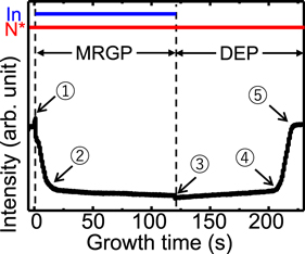
Fig. 13. (Color online) The In beam (blue) and N radical beam (red) supply programs for each DERI cycle are shown in the upper half of the figure. ① Each DERI cycle starts at this point. The InN surface is N-stabilized. ①-② The InN surface is covered by In and the surface changes from N-stabilized to In-stabilized. ② The InN surface is covered by 2 ml of In. ②-③ Additional accumulation of In then formation of In droplets. The number and size of droplets increase. ③ The In supply is shut off and DEP starts. ③-④ The number and size of In droplets decrease. ④ The surface is covered by 2 ml of In. ⑤ The In wetting layer thickness reduces and is totally consumed. The surface of InN changes from In-stabilized to N-stabilized. (Reproduced from Ref. 30.)
Download figure:
Standard image High-resolution imageThe laser reflection intensity has also been monitored for about 2 h using the DERI process with a completely separate In and nitrogen supply mode. In each growth cycle, the In supply time is 30 s and the N radical supply time is 60 s, and this supply mode is repeated for 80 cycles, as shown in Fig. 14(a). 32) This envelope of the signal demonstrates a clear intensity oscillation with long intervals, which is due to interference between the reflected laser beams from the top surface and the GaN/InN interface. The damping of the amplitude of oscillation is due to the absorption of 660 nm laser light by the growing InN layer with narrower band gap energy than that of 660 nm laser light. A zoomed-in figure of this laser reflection intensity variation is shown in the upper half of Fig. 14(b), with the corresponding RHEED intensity variation in the lower half. 32) The laser reflection intensity is also sensitive to the surface coverage conditions and changes according to each DERI cycle. However, how each intensity increases and decreases is just the opposite of the other's. 32)

Fig. 14. (Color online) (a) Laser reflection intensity variations during 80 cycles of DERI process. The envelope of the signal is due to interference between the reflected laser beams from the top surface and the GaN/InN interface. The damping of the amplitude of oscillation is due to the absorption of 660 nm laser light by the growing InN layer. (b) A zoomed-in view of the laser reflection intensity variation is shown on top (red line) and the corresponding RHEED intensity variation is shown below (black line). (Reproduced from Ref. 32.)
Download figure:
Standard image High-resolution imageThe laser reflection intensity variation was carefully monitored by increasing the deposition time of In, corresponding to an increase in the number of In adatoms supplied on the growing surface. Figure 15 suggests that the structure of the In wetting layer and droplets on the surface change to the next step as coverage increases to a point higher than a certain threshold. 32)
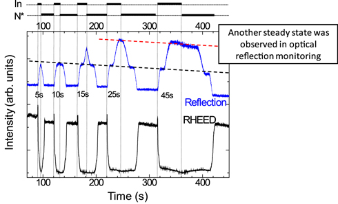
Fig. 15. (Color online) Laser reflection intensity variation monitored with increasing deposition time of In. The position and structure of the In wetting layer on the surface change to the next step as coverage increases to a point higher than a certain threshold. (Reproduced from Ref. 32.)
Download figure:
Standard image High-resolution imageTherefore, the laser reflectivity signal is able to provide complementary information to RHEED for in situ monitoring of the InN growth process. The RHEED signal reveals a crystalline surface structure. However, when metallic In is deposited on the surface, the RHEED intensity becomes very weak and can hardly reveal such a deposition process except an abrupt drop in its intensity. On the other hand, the laser reflection signal is very sensitive to the conditions of metal coverage and formation of In droplets. Consequently, a strong contrast can be seen between the laser reflection and RHEED signals.
The growth rate can be extracted from the interference oscillation shown in Fig. 14. A laser beam with a 660 nm wavelength makes interference with every 122 nm increase in InN film thickness assuming the reflective index of InN is 2.7. During this 122 nm growth corresponding to one laser beam interference cycle, 30 cycles of the DERI process are repeated. Therefore, an InN film grown in one DERI cycle can be estimated to be 4.1 nm. This estimation is also confirmed by ex situ cross-sectional SEM measurements, which show a total 330 nm growth for 80 cycles.
In supply for one cycle during 30 s of MRGP is equivalent to 4.1 nm thick InN. The time required for surface coverage by In is 4.5 s from RHEED variation. Then, the amount of In supplied to cover the InN surface can be estimated to be equivalent to 0.615 nm thick InN, which theoretically equals to 4.1 × 4.5/30 nm. This amount of In supplied for surface coverage almost agrees with two equivalent monolayers of InN, as the c lattice constant of InN, which consists of two monolayers of InN, is 0.570 nm. This result is reasonable when theoretical calculation 33) is taken into account, where Ga metal covers the GaN surface with a laterally contracted form. An additional peak in laser reflection intensity, observed in Fig. 15, probably comes from the formation of In droplets after covering the InN surface by two monolayers of In.
Theoretical 33) and experimental studies 34,35) on the adsorption and desorption of Ga on GaN have been extensively carried out to investigate the growth mechanisms of GaN by RF–MBE using Q-mass 34) and RHEED. 35) These studies suggest a stable double monolayer of Ga on the GaN surface as a wetting layer and an additional supply of Ga cause the formation of Ga droplets. In situ monitoring by RHEED and laser beam reflection during our DERI process of InN also suggests the existence of a double monolayer of the In wetting layer and the formation of In droplets after an additional In supply.
Accordingly, InN growth by our DERI process can be explained as follows. During MRGP, In covers the substrate surface until stable two monolayers of In are formed. An additional supply of In causes the formation of In droplets. As soon as DEP starts with cutting off the In supply, reaction of N radicals with wetting In starts either at the kink site or on the step edge of the growing surface. In order to keep stable surfaces with two monolayers of In, consumed In by reaction with N radicals to form InN is re-supplied from the In droplet reservoir after migrating on the growing surface. Thus, layer-by-layer growth of InN proceeds by keeping thermally stable two monolayers of wetting In. This process gradually decreases the size of the In droplets until they eventually disappear. As growth proceeds with a continued supply of N radicals, the wetting layer changes from two to one monolayer and finally all In on the surface completely dries out and the N-stabilized surface recovers. This concludes DEP and the next cycle of MRGP starts again with the start of In supply.
Thus, the DERI process can be recognized as a kind of atomic-level LPE process. It is widely known that the LPE process is carried out under very close to thermal equilibrium conditions. In addition to the regular LPE process, the DERI process by RF–MBE has given an additional advantage for atomic-level thickness control. When this thermal equilibrium process is considered, one can explain the reason why high-quality InN can be grown reproducibly by the DERI method, compared with the conventional growth process by RF–MBE.
10. Growth of InGaN and multiple quantum wells
The DERI process was applied for the growth of InGaN. The strong dependence of alloy composition on N radical intensity was observed as shown in Fig. 16. 31) Here, the supplied beams of Ga and In are all kept constant throughout this growth experiment. InGaN grown under N-rich conditions with RF power higher than 450 W showed almost the same InGaN alloy composition as the In/Ga supply rate. On the other hand, with InGaN grown under 100 W of RF power, GaN and InN are grown almost separately—GaN growth first, followed by InN growth.
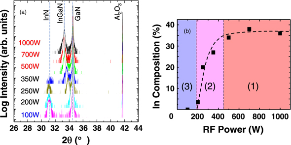
Fig. 16. (Color online) (a) XRD 2θ–ω profile dependence on input RF power. (b) In composition dependence on input RF power. InGaN grown under N-rich conditions (1) with RF power higher than 450 W shows almost the same InGaN alloy composition as the In/Ga supply rate. The alloy composition changes remarkably in region (2). GaN and InN are grown almost separately in region (3). (Reproduced from Ref. 31.)
Download figure:
Standard image High-resolution imageA remarkable change in alloy composition is observed in the intermediate RF power zone in Fig. 16. 31) The result comes from a strong preferential GaN solidification over InN, and In in an In–Ga wetting layer is swept out from the growth front. This can be explained by a much stronger chemical bond between Ga and N compared with that between In and N. This preferential capture is more favorable as solidification from metal solution to solid phase proceeds under thermal equilibrium conditions like those in the DERI process.
As a result, the InN molar fraction x of InxGa1-xN grown under N-rich conditions is determined by the supply rate and explained in the form of

where  and
and  are the beam flux intensity of Ga and In, respectively.
On the other hand, the InN molar fraction x of InxGa1-xN grown under metal-rich conditions is explained by

It should be noted that alloy composition is determined by the supply rate of Ga and N radicals and not by the In supply rate.
The relation between alloy composition and growth temperature with FGa as a parameter is shown in Fig. 17. Based on these conditions, InGaN films with full alloy compositions from GaN to InN are successfully obtained by the DERI method. 36)

Fig. 17. (Color online) Relation between alloy composition and growth temperature with FGa as a parameter.
Download figure:
Standard image High-resolution imageUnder metal-rich conditions, the total supply of metal (FGa + FIn) is larger than the nitrogen flux. As a result, the In wetting layer and droplets remain on the surface after solidification of the InGaN alloy. During DEP by an only N radical beam supply, InN film grows on top of InGaN. An InN/InGaN multiple quantum well (MQW) structure can be formed by repeating this DERI cycle. 37)
Successful formation of an MQW structure has been confirmed by high-angle annular dark-field scanning TEM (HAADF-STEM) and X-ray diffraction (XRD) with high-order satellite peaks, as shown in Fig. 18. 38) The PL from this MQW is shown in Fig. 19. 38) This PL intensity is much stronger than that from MQWs obtained by conventional RF–MBE. 39) These results indicate a clear advantage of the DERI method over conventional methods in terms of quality and reproducibility.

Fig. 18. (Color online) (a) Cross-sectional view of MQW observed by HAADF-STEM and (b) corresponding XRD 2θ–ω profile with high-order satellite peaks (reproduced from Ref. 38).
Download figure:
Standard image High-resolution image
Fig. 19. (Color online) PL from MQW structure in Fig. 18 shown as a red line. The PL without MQWs is also shown by a black line for comparison. (Reproduced from Ref. 38.)
Download figure:
Standard image High-resolution image11. In situ measurements during InGaN growth
Availability for various kinds of in situ observation is one of the biggest advantages of MBE. As plasma-excited MBE involves many kinds of excited neutral and ionized atoms and molecules in its growth process, these kinds of in situ observation are very important to understanding the growth process. Measurements by OES, RHEED, and laser beam reflection have given various useful information as has been mentioned in this paper.
In situ X-ray reciprocal space mapping measurements have been carried out connecting a high-power X-ray beam supplied from SPring-8 facilities and an RF–MBE growth system. 40) Alloy composition and strain relaxation in InGaN were estimated from in situ measurements and compared for growth on GaN templates and InN templates. Results have shown a strong pulling effect in alloy composition with Ga-rich InGaN growth on GaN and In-rich InGaN growth on InN, as shown in Fig. 20. 41) This result implies requirement of careful consideration on the pulling effect for accurate design and fabrication of heterostructures for quantum-size devices consisting of InGaN, GaN and InN.

Fig. 20. (Color online) Evolution of In composition (red) and relaxation ratio (purple) of InGaN during growth on (a) GaN template and (b) InN template, determined by in situ X-ray reciprocal space mapping (reproduced from Ref. 41).
Download figure:
Standard image High-resolution image
Studies on in situ X-ray reciprocal space mapping have also been carried out during InGaN growth on InN at elevated temperature. 42) Results show signs of intermixing during growth. This information gives us the highest possible growth temperature to obtain abrupt interfaces in the atomic level.
12. Device applications of RF–MBE and future prospects
It is widely known that hetero-interfaces grown by MBE are generally sharper and flatter than those grown by MOCVD due to MBE's capability for atomic layer level growth control. The two-dimensional electron gas formed between AlGaN and GaN by RF–MBE shows better quality with higher mobility 43,44) than that formed between films grown by MOCVD. An InGaN/InN structure has the potential to supply even higher mobility two-dimensional electron gas. Thus, RF–MBE has strong potential to supply two-dimensional electron gas with high mobility, which can be applied in future high-frequency and high-speed devices. Research and development of advanced devices which use the full potential of nitride-based material properties should re-evaluate RF–MBE technology when large-size freestanding GaN substrates become available with lower cost, as we can then expect to achieve a heterostructure with an ideal interface.
Application of RF–MBE to nitride-based laser diodes has been extensively carried out at TopGaN in Poland. CW operation in the 410 to 482 nm range with a lifetime exceeding 2000 h has already been reported. 45)
In MOCVD, p-type doping to GaN and related nitride semiconductors by Mg has very serious problems due to the passivation of Mg by hydrogen. As RF–MBE does not use NH3 as a nitrogen source, we do not need to be concerned about Mg passivation by hydrogen. Therefore, p-type doping conductivity is achieved without the post-growth activation process. Taking this advantage, a true-blue (450 nm) laser diode with tunnel junctions grown monolithically by RF–MBE has been reported. 46) The intrinsic difficulty in the MOCVD growth of tunnel junctions arises from the fact that hydrogen cannot diffuse through n-type layers by post-annealing. Hybrid regrowth of n-type layers by RF–MBE on pre-activated MOCVD-grown p-type GaN also offers a new process of making laser diodes with sophisticated structures based on GaN and InGaN.
InN and In-rich InGaN are material systems with very high potential for both optoelectronic and high-frequency electronic devices. However, practical devices have not been reported yet. One of the main reasons which hinder device application is the existence of high-density accumulated electrons on the surface. 47) P-type doping by Mg to InN and hole activation themselves are already confirmed by capacitance–voltage (C–V) measurements using the electrochemical method. 48,49) However, the surface of p-type-conducting InN is always surrounded by an n-type layer with the accumulated high-density electrons. Thin epitaxial films with wider band gap material like InGaN or AlInN prepared by RF–MBE may solve this persistent problem of InN surface accumulation layers.
The active region in actual electronic and optoelectronic devices is usually very thin or very small in size with a nanometer scale. The selective regrowth process by plasma-excited MBE may become a powerful method to fabricate these structures. Hybrid use of ECR–MBE and RF–MBE may offer this kind of process, utilizing the functions of ions and radicals selectively.
13. Summary
Our proposal and the following advancements of plasma-excited MBE are reviewed. We proposed connecting an ECR plasma source with a divergent magnetic field and MBE more than 35 years ago. Owing to its ability to supply highly excited ions and radicals to substrates, successful low-temperature substrate cleaning and subsequent low-temperature growth of GaAs has been achieved. This proves its high potential as a regrowth method for nanoscale quantum-size devices.
Low-energy and high-density ions generated in ECR plasma are responsible for selective-area growth. On the other hand, high-density radicals are found to be responsible for epitaxial growth itself.
Then, ECR–MBE was applied to low-temperature GaN growth, where the growth temperature is limited at the dissociation temperature of NH3 for MOCVD. Due to its capability for low-temperature growth, successful growth of GaN on silica glass was demonstrated. With careful control of the impinging energy of ions on the growing surface by changing the bias voltage to the substrate, it was demonstrated that the effective V/III ratio on the growing surface can be controlled electrically. Possible growth of superlattices consisting of cubic and hexagonal phases is proposed where only bias voltage to the substrate is modified. Successful growth of position-controlled InN nano-columns also became possible by controlling the impinging energy of ions to the substrates.
High-quality InN growth became possible after we applied RF–MBE, where low-temperature growth with a precisely controlled V/III ratio was found to be essential. The true band gap of InN was found and revised to around 0.7 eV from the long-believed value of 1.9 eV. Other fundamental physical properties, like effective mass, were also revised after characterization of high-quality InN grown by RF–MBE. These new findings on the basic physical properties of InN and In-rich InGaN became possible only after high-quality InN was obtained by plasma-excited MBE.
The DERI method is proposed for reproducible growth of high-quality InN, where stringent control of the V/III ratio is required all through the growth process. RF–MBE with the DERI process should open up new possibilities for devices based on InN and In-rich InGaN. Growth of high-quality InGaN/InN MQW structures was successfully achieved by just repeating DERI cycles.
RF–MBE is already successfully applied in the fabrication of practical laser diodes based on InGaN and GaN. Capability for Mg doping without annealing for activation is a big advantage of RF–MBE over other growth methods. Taking this advantage, a monolithically grown true-blue laser diode with a tunnel junction has already been reported.
Plasma-excited MBE with its unique advantages over other growth methods should pave the way for new device structures and processes for future development of optoelectronic and high-frequency electronic devices based on GaAs, GaN, InN and related compounds and alloys.
Acknowledgments
The authors thank all colleagues, students and staff at NTT Research Laboratory and Ritsumeikan University for their contributions throughout this research. The authors also thank Prof. Tadeusz Suski and Prof. Czeslaw Skierbiszewski of the Polish Academy of Science for useful discussions. We also acknowledge continued financial support from MEXT as Grants-in-Aid for Scientific Research.