
Abstract
InGaN-based LEDs are efficient light sources in the blue–green light range and have been successfully commercialized in the last decades. Extending their spectral range to the red region causes a significant reduction in LED efficiency. This challenge hinders the integration of red, green, and blue LEDs based on III-nitride materials, especially for full-color micro-LED displays. We review our recent progress on InGaN-based red LEDs with different chip sizes from hundreds to tens of micrometers, including the epitaxial structures, device fabrication, and optical performance (peak wavelength, full-width at half-maximum, light output power, efficiency, temperature stability, and color coordinates).
Export citation and abstract BibTeX RIS

Content from this work may be used under the terms of the Creative Commons Attribution 4.0 license. Any further distribution of this work must maintain attribution to the author(s) and the title of the work, journal citation and DOI.
1. Introduction
III-nitride semiconductors have a direct bandgap and their alloys can cover a wide spectral range from deep UV to near-infrared. 1–4) The tremendous success of III-nitride semiconductors is the invention and development of efficient InGaN-based blue/green LEDs, 5–7) which have been commercialized for many years and are widely used in illumination and display applications. 8–10) To date, violet and blue InGaN-based LEDs have achieved a high wall-plug efficiency (WPE) of 84% and 81%, respectively. 11,12) Also, green InGaN-based LEDs for 534 nm emission can reach a peak WPE of 56%. 13) These typical values demonstrate that InGaN alloys are an excellent material system for efficient visible light sources.
Recently, beyond liquid crystal display and organic LED display, InGaN-based micro-LEDs (μLEDs) have gathered great interest in the applications of next-generation high-performance displays including large-area screens and smart wearable consumer electronics. 14–17) This μLED display technology requires individual red–green–blue (RGB) μLEDs as a single-pixel for full-color displays. Two feasible approaches are proposed to realize RGB μLEDs. A simple method utilizes violet or blue μLEDs to excite the color converters, such as phosphors or quantum dots (QDs). 18–21) However, the photoluminescence mechanism used in this method is related to several intermediate steps, which possibly lead to the loss of energy during the color conversion. 21,22) Therefore, the color-conversion efficiency must be improved.
Another method realizes the RGB colors by the electroluminescence (EL) of μLEDs. In this method, RGB μLED chips must be realized individually. Currently, most blue and green LEDs are made of InGaN materials, but the red LED chips are made of aluminum gallium indium phosphide (AlGaInP) material. The large-size AlGaInP red LEDs have a high WPE above 50%. However, when the device dimensions shrink to the size of μLEDs, the efficiency drops dramatically because of the high surface recombination and long carrier diffusion lengths. 23–25) The efficiency of AlGaInP red LEDs is also very sensitive to the junction temperature. The high operation temperature will cause significant carrier leakage through AlGaInP red LEDs, leading to an obvious efficiency thermal droop. 26) Also, when integrating RGB μLEDs, researchers observed mismatched light angular distributions because of the material difference between InGaN blue/green and AlGaInP red μLEDs. 27) This mismatched light angular distribution causes a noticeable color shift at different observed angles, which is unfavorable for micro-displays.
Therefore, extending the emission wavelength of InGaN-based LEDs from blue/green to red seems to be a good choice to replace AlGaInP red μLEDs for micro-displays. However, achieving red emission requires a high-In-content above 0.3 in the quantum wells (QWs), which is quite challenging due to the large lattice mismatch between InN and GaN. 28) A high number of defects would be generated during the growth of high-In-content InGaN QWs, which would dramatically degrade the device performance. In addition, the well-known quantum-confined Stark effect (QCSE) becomes severe in high-In-content InGaN QWs, which lowers the spontaneous recombination rate due to the spatial separation of the electron and hole wavefunctions. 29,30)
Some potential substrates like ZnO 31) and ScAlMgO4 32) were proposed due to their lattice matching with InGaN (In content ~0.17–0.18) layers. However, growth on these substrates by metalorganic vapor-phase epitaxy (MOVPE) was very challenging because the ZnO and ScAlMgO4 substrates would decompose during the high-temperature growth for nitride materials.
High-In-content InGaN growth also has other alternatives. For example, semi-polar or N-polar surfaces are demonstrated to favor In incorporation into GaN. 33,34) Therefore, some groups chose these GaN surfaces to realize long-wavelength emission of InGaN-based LEDs from amber to red. 35–38) Also, red luminescence could be realized by GaN with europium doping. By the stacking of 100 pairs of GaN/GaN:Eu layers, a maximum external quantum efficiency (EQE) of 9.2% was reported for this system. 39) The 1 nm FWHM with the emission wavelength of 621 nm for GaN:Eu LEDs indicated that the purity of the red emission was 100%. 40)
Nanowire or nanocolumn structures are another promising candidate for InGaN-based red LEDs. 41) They can neglect the polarization field in InGaN QWs and help to integrate RGB LEDs on the same wafer. 42,43) A special InGaN template named InGaN platelets was demonstrated to have relaxed lattice constants, which enabled the shifting of the QW emission from blue to green and red. 44) In addition, InGaN QDs presented great potential for red LEDs because they could exhibit improved crystalline quality due to the strain relaxation and suppress the QCSE for InGaN growth with high In composition. 45)
However, realizing c-plane InGaN-QW-based red LEDs is still the best choice because they are compatible with current production lines. All the mature technologies of InGaN-based blue/green LEDs can survive with minimal modification. Therefore, our group focused on the realization of c-plane InGaN-QW-based red LEDs. In this review, we will summarize our recent progress in the development of InGaN red LEDs. Because LED chip size is an important parameter based on different applications, we separated the main context of this review into two parts: large-size LEDs and μLEDs. In each part, we covered the structures and the device performance of InGaN-based red LEDs. At the end, we presented a short conclusive remark about our work and some prospects in InGaN-based red LEDs.
2. InGaN red large-size LEDs
InGaN large-size LEDs are the traditional device chips with dimensions in the hundreds of micrometers to several millimeters. In 2012, Ohkawa et al. reported a novel high-temperature growth technique to grow high-quality and high-In-content InGaN layers. 46) They demonstrated large-size LEDs with a long-wavelength EL peak emission of 740 nm. 47) In 2014, Hwang et al. reported the demonstration of a c-plane InGaN-based red LED with a light output power of 1.1 mW with a wavelength of 629 nm at 20 mA and 4.4 V. 48) The EQE and WPE of their red LEDs at 20 mA were 2.9% and 1.3%, respectively. Recently, a full InGaN structure, starting from a relaxed InGaN pseudo-substrate to a p-doped InGaN layer, was used to achieve red LEDs. 49) The FWHM of this full InGaN LED at 0.8 A cm−2 was 48 at 630 nm, which was regarded as a true red emission. Also, Zhang et al. successfully developed a series of efficient InGaN-based orange and red LEDs on Si, with peak wavelengths from 594 to 621 nm and peak WPEs from 30.1% to 16.8% at 0.8 A cm−2. 50)
Recently, our group proposed strain-compensation strategies by introducing AlN/AlGaN barriers 51) and hybrid QWs 52) for the high-In-content InGaN growth. These structures were able to reduce defects in QWs and finally enhance the light output power of amber and orange LEDs. Based on these growth techniques and active region structures, we moved forward to investigate the different templates and optimize the device fabrication process for InGaN red LEDs.
In this section, we first reviewed our epitaxial structures and device fabrication process, then discussed the performance of InGaN red LEDs.
2.1. Realization of red LEDs
2.1.1. Epitaxial growth and LED structures
Our InGaN-based red LED epitaxial wafers were grown by MOVPE in a single-wafer horizontal reactor at 100 kPa. Trimethylgallium (TMGa), trimethylaluminum (TMAl), trimethylindium (TMIn), and ammonia (NH3) are used as Ga, Al, In, and N sources, respectively. The n- and p-type doping precursors were N2-diluted silane and bis(cyclopentadienyl)magnesium (Cp2Mg), respectively. The carrier gases during MOVPE growth were high-purity H2, N2, or their mixtures.
The epitaxial growth structure of InGaN-based red LEDs is shown in Fig. 1(a). A c-plane GaN film is utilized to serve as a template for InGaN visible LED growth. However, GaN and high-In-content InGaN have a large lattice mismatch, which would cause many defects and degrade the quality of InGaN layers. Because the lattice mismatch was related to the in-plane strain of the epitaxial layers, understanding the influence of the GaN templates' in-plane strain helped to improve the crystal quality of high-In-content InGaN layers.

Fig. 1. (Color online) (a) Schematic of an InGaN-based red LED epitaxial structure. (b) Cross-sectional high-resolution transmission electron microscope (HRTEM) image of an InGaN-based red LED.
Download figure:
Standard image High-resolution imageThere are two different ways to adjust the in-plane strain of GaN templates. One is to adjust the thickness of GaN templates, and the other is to choose GaN templates on different substrates. In our study, we investigated different GaN templates on c-plane patterned sapphire substrates (PSS) and Sn-doped β-Ga2O3 substrates. 53,54) The GaN templates on PSS were prepared by our MOVPE system, and we grew different thicknesses from 4 to 10 μm for the GaN templates. The GaN growth rate was around 2.4 μm h−1. The n-type GaN template on an Sn-doped β-Ga2O3 substrate was purchased from Tamura Co. and Novel Crystal Technology, Inc. SiNx arrays were used at the interface between the GaN template and Ga2O3 substrate, which could enhance the light extraction efficiency and enable the carrier conductivity at the interface. 55,56) Both of the FWHMs of (0002) and (10–12) planes X-ray rocking curve for GaN templates on PSS and Ga2O3 were below 300 arcsec, revealing good crystal quality of the GaN templates.
We regrew 1 μm thick n-Al0.03Ga0.97N or n-GaN on the GaN templates on PSS and Ga2O3 substrate, respectively. The n-Al0.03Ga0.97N layer was able to realize a smooth surface and a lower series resistance by high Si doping. Then, 15 pairs of In0.08Ga0.92N (2–2.5 nm)/GaN (5.5–6 nm) superlattices (SLs) were grown on the n-type layer, followed by a 15 nm thick n-GaN. The active region consisted of two components: a single blue In0.2Ga0.8N QW and two red InGaN QWs. This hybrid multiple QWs in our previous work have been shown to help improve light output power. 52) The In content in red QWs was adjusted by the growth temperature.
Also, we proposed complicated barrier layers [Fig. 1(a)] for strain compensation. 51,53) The red QWs grown on the Al0.13Ga0.87N barrier layer could obtain fewer trench defects and realize a better crystal quality, which contributed to an enhanced device performance. The capping layer was GaN and AlN for the blue and red QWs, respectively, which were grown at the same temperature as QWs. The AlN interlayer could suppress the decomposition of the high-In-content red QWs during the barrier layer growth at higher temperatures. 48) Finally, a 100 nm thick Mg-doped p-GaN layer and a 10 nm thick heavily Mg-doped p+-GaN layer were grown on top of the active region.
Figure 1(b) shows a typical cross-sectional HRTEM image of our InGaN red LED structure. The LED structure could be seen clearly in this HRTEM image, demonstrating the same structure that we designed. The sharp contrast between InGaN and barrier layers in the active region and SLs indicated an abrupt interface of the structures.
2.1.2. Indium tin oxide (ITO) optimization for device fabrication
After epitaxial growth, device fabrication is a further important step to realize high-performance InGaN red LEDs. Due to the low doping level and high work function of the p-GaN layer, high-quality p-GaN contacts are always the key issue for device performance. ITO is one of the most popular materials for the transparent p-electrode in InGaN-based blue and green LEDs. 57,58) It is usually deposited by e-beam evaporation or magnetron sputtering. 59,60) However, the deposition process is generally carried out in an oxygen atmosphere at high temperatures, which are complicated and require additional configurations for facilities. 59,61) In addition, little attention has been paid to the optimization of ITO layers for InGaN-based LEDs in the red region. Therefore, the ITO layer for InGaN red LEDs needs further optimization.
We proposed a two-step annealing process under O2-containing (Ar/O2 mixture) and O2-poor (Ar) atmospheres in sequence. 62) Figure 2(a) shows the sheet resistivity of ITO layers on double-polished sapphire substrates. The samples named S1–S3 were sputtered ITO while the sample named E1 was e-beam evaporated ITO. All the deposition processes were at room temperature (RT) without oxygen gas. As shown in Fig. 2(a), the two-step annealing could reduce the sheet resistivity of sputtered ITO to around 2 × 10⁻⁴ Ω cm. These results could be explained by the conductivity mechanism of ITO layers, which were related to oxygen vacancies. 60) Also, the transmittance of ITO layers could be improved after the two-step annealing, reaching over 98% for sputtered ITO in the 590–780 nm wavelength range [Fig. 2(b)]. As a result, we demonstrated that the two-step annealing indicates the excellent performance of ITO in the aspect of conductivity and transmittance.

Fig. 2. (Color online) (a) Sheet resistivity of sputtered ITO (S1–S3) and e-beam evaporated ITO (E1) under different annealing processes. (b) Transmittance of sputtered and e-beam evaporated ITO layers before and after two-step annealing. (c) Current dependence of the light output power of red LEDs with sputtered and evaporated ITO, respectively. The inset was an EL emission picture of one red LED chip with sputtered ITO at 20 mA. (c) is reproduced from Ref. 62 with the permission © The Optical Society.
Download figure:
Standard image High-resolution imageMeanwhile, we found that sputtered ITO exhibited better conductivity and higher transmittance than e-beam evaporated ITO, as shown in Figs. 2(a) and 2(b). This comparison result was attributed mainly to the crystal quality of ITO layers, which was characterized by the XRD diagram in our previous work. Finally, we utilized sputtered and e-beam evaporated ITO to fabricate red LEDs. Figure 2(c) shows the light output power of the red LEDs at different currents. The red LEDs with sputtered ITO were demonstrated to have a higher light output power as compared to those LEDs using e-beam evaporated ITO. This result was reasonable based on the performance comparison of sputtered and e-beam evaporated ITO in Figs. 2(a) and 2(b).
2.2. Optical properties of InGaN red LEDs
Based on the epitaxial growth and device fabrication techniques, we investigated the optical properties of InGaN red LEDs. The section was separated into three parts: the influence of the strain of GaN templates, the effect of LED chip sizes, and the temperature stability.
2.2.1. Influence of the strain of GaN templates
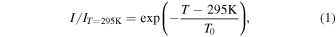
We measured the in-plane residual stress of the different GaN templates, as shown in Fig. 3(a). The in-plane residual compressive stress of the GaN on PSS was gradually reduced as the GaN thickness was increased from 4 to 10 μm. Also, in the case of GaN on Ga2O3 substrate, the 5 μm thick GaN template exhibited a few in-plane tensile or compressive stresses. The error bar was due to the use of different Raman shift values of the free-standing GaN from different Refs. 63, 64. Therefore, we could conclude that Ga2O3 substrates help relax the residual stress for the GaN template compared to PSS.

Fig. 3. (Color online) (a) In-plane residual stress of GaN templates on PSS and Ga2O3. The negative symbol means the compressive stress. (b) EL peak wavelength and (c) EL intensity of red LEDs at 20 mA as functions of the in-plane stress in the GaN templates. The dashed lines are the average values. (d) EL spectra of red LEDs based on the GaN templates on PSS and Ga2O3 at 20 mA. The insets are the emission pictures of red LEDs on PSS and Ga2O3 at 20 mA, respectively. (b)–(c) are reproduced from Ref. 53 (CC BY 4.0). The insets in (d) are reproduced from Ref. 53 (CC BY 4.0) and 54 (CC BY 4.0).
Download figure:
Standard image High-resolution imageFigure 3(b) shows the EL peak wavelength of InGaN red LEDs on the GaN templates on PSS with different residual in-plane stresses. The MOVPE growth conditions were the same for all samples. Clearly, the peak wavelength gradually red-shifted as the in-plane residual stress decreased. This phenomenon indicated that In incorporation was enhanced due to the relaxed in-plane residual stress in the underlying GaN layers. As a result, we can make a higher growth temperature of InGaN red QWs by using a thicker GaN template for the same emission wavelengths. Based on our experiments, 53) the increment of the growth temperatures for the case of GaN thicknesses of 4 and 10 μm was around 5 °C.
We realized the same peak wavelength of 635 ± 2 nm for red LEDs on GaN templates with different in-plane residual stresses by adjusting the growth temperature. As shown in Fig. 3(c), the EL intensity could be enhanced 1.3 fold because of the higher growth temperature for InGaN red QWs on more relaxed GaN templates. Another reason for the enhancement was that the possibility of the defect formation might also be reduced in the active region due to the lower lattice mismatch between the InGaN red QWs and the GaN templates.
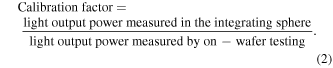
Meanwhile, we compared the EL emission for red LEDs on PSS and Ga2O3 in Fig. 3(d). Although the QW growth temperature for the Ga2O3 substrate was 15 °C higher, the peak wavelength of red LEDs on Ga2O3 (665 nm) exhibited a large red-shift of 32 nm at 20 mA compared to LEDs on PSS (633 nm). This result further demonstrated that less in-plane residual compressive stress helped enhance the In incorporation. Figures 4(a) and 4(b) show the light output power and EQE of red LEDs, respectively. All the LEDs in our measurements were bare chips without resin encapsulation. The red LEDs on PSS exhibited a better performance, which originated from the lower In content in red QWs compared to LEDs on Ga2O3. The light output power of red LEDs on PSS could achieve 1 mW at a current of 30 mA. The EQE of red LEDs on PSS and Ga2O3 was 1.6% and 0.19% at 20 mA, respectively. In addition, the forward voltage of red LEDs on PSS and Ga2O3 at 20 mA was 3.3 and 2.45 V, respectively. So the WPE of red LEDs on PSS and Ga2O3 at 20 mA could be calculated as 1.0% and 0.14%, respectively.

Fig. 4. (Color online) (a) Light output power and (b) EQE as functions of the injection current for InGaN-based red LEDs on PSS and Ga2O3.
Download figure:
Standard image High-resolution image2.2.2. The effect of LED chip size
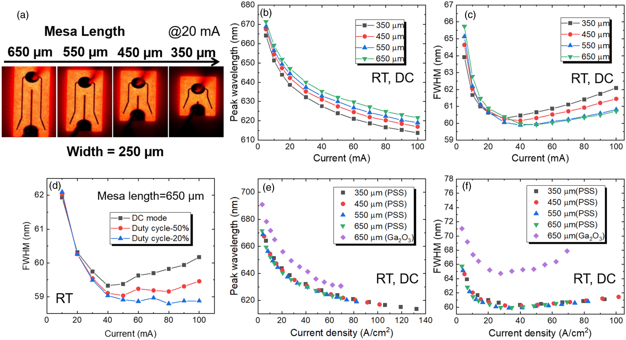
Furthermore, we investigated the effect of chip size on the optical performance of red LEDs on PSS. 65) We fabricated rectangular LED chips with different mesa areas, as shown in Fig. 5(a). The mesa width kept constant as 250 μm, while the mesa length reduced from 650 to 350 μm. So the active areas were calculated to be 0.1445, 0.1215, 0.0985, and 0.0755 mm2, respectively. The EL images in Fig. 5(a) demonstrated that all chips exhibited homogeneous emission and had no significant current crowding. However, we also observed many dark spots in the emission area, which were regarded as threading dislocations or trench defects.

Fig. 5. (Color online) (a) EL emission images of red LEDs on PSS with different mesa lengths from 650 to 350 μm at 20 mA. Current dependences of (b) peak wavelength and (c) FWHM of red LEDs on PSS with different mesa lengths. Each point is an average from over 10 LEDs for each mesa length. (d) Current dependence of FWHM of a red LED on PSS operated at direct current (DC) and pulsed current mode. Current density dependence of (e) peak wavelength and (f) FWHM of red LEDs on PSS and Ga2O3. (a)–(c) are reproduced from Ref. 65 (CC BY 4.0).
Download figure:
Standard image High-resolution imageThe peak wavelengths of red LEDs at 5–100 mA are shown in Fig. 5(b). An approximately 50 nm blue-shift was observed for all chips with different chip sizes. The blue-shift amount for red LEDs was much higher than that for the blue and green LEDs, illustrating a very strong QCSE in InGaN red QWs. Also, smaller chips had a blue-shift compared to larger chips at the same current injection. This phenomenon was reasonable because of the screening of QCSE by a higher current density in smaller chips. Generally, LEDs would be operated at a certain current for a designed peak wavelength. Because the emission wavelength also depended on the chip sizes, researchers should consider the In content in red QWs and design the chip size together.
The FWHM dropped rapidly to the minimum values (around 60 nm) in the low current range and then increased slightly with currents in Fig. 5(c). The current dependent behavior of the FWHM was similar for all chip sizes. However, the smaller chips exhibited narrower FWHM at low currents but became broader at high currents when compared to those larger chips. This phenomenon was related to the two different mechanisms for the variation of FWHM. The narrowing of the FWHM was attributed to the filling of deep localized states, while the broadening of the FWHM originated from heat generation. 37,66) As shown in Fig. 5(d), the duty cycle of the pulsed currents would determine the FWHM at high currents, which demonstrated that the heat generation was the main reason for the broadening of FHWM. Therefore, the higher current density for smaller chips would accelerate the filling of deep localized states to make the FWHM narrower, but generated more heat within chips to make the FWHM broader.
Interestingly, the peak wavelength and FWHM for different chips followed the identical current density dependence, as shown in Figs. 5(e) and 5(f). These results indicated that the residual strain and localized states in red QWs remained constant after fabrication. Also, the peak wavelength and FWHM of red LEDs on Ga2O3 were plotted in Figs. 5(e)–5(f) for comparison. The red LEDs on Ga2O3 exhibited a total blue-shift of 60 nm, which was 10 nm larger than that of red LEDs on PSS. The FWHM of red LEDs on Ga2O3 also increased by 5–7 nm at the same current density compared to red LEDs on PSS. These results illustrated that the QCSE and In fluctuation would become more severe upon a further increase of the In content in red QWs, 67) which explained the performance degradation of red LEDs on Ga2O3 in Fig. 4.
2.2.3. Temperature stability of red LEDs
The temperature dependence of the EL intensity for InGaN-based red LEDs on PSS and Ga2O3 was measured at a probe station. The stage temperature was controlled by a heater from 295 K (RT) to 373 K. Figure 6(a) shows the normalized EL intensity at different stage temperatures at 100 mA. The EL intensity dropped as the temperature increased, which is usually called the thermal droop. 68) The thermal droop could be described by the following formula 48,65)
where I/IT=295K is the normalized EL intensity by the EL intensity at 295 K, T [K] is a stage temperature, and T0 [K] is the characteristic temperature.

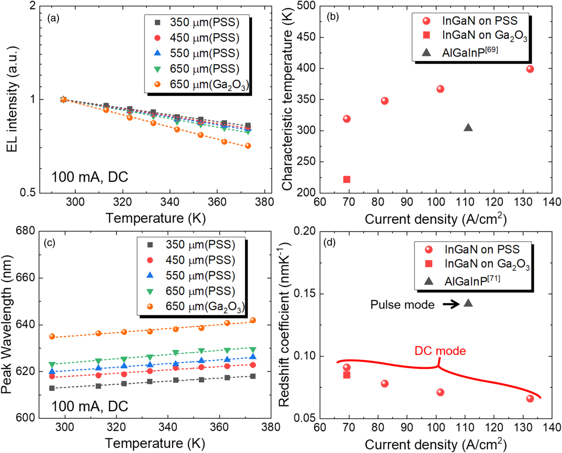
Fig. 6. (Color online) (a) Temperature dependence of normalized EL intensity of InGaN red LEDs on PSS and Ga2O3 at a direct current of 100 mA. (b) The characteristic temperature of InGaN and AlGaInP red LEDs at different current densities. (c) Temperature dependence of the peak wavelength of InGaN red LEDs on PSS and Ga2O3 at a direct current of 100 mA. (d) Red-shift coefficients of InGaN and AlGaInP red LEDs at different current densities.
Download figure:
Standard image High-resolution imageThe characteristic temperature is usually regarded as a standard quantitative parameter to evaluate the temperature stability of LEDs. A larger characteristic temperature implies better temperature stability in the LED light output. By using Eq. (1) to fit the data points in Fig. 6(a), we obtained the characteristic temperatures at various current densities in Fig. 6(b). The characteristic temperature of AlGaInP red LEDs 69) was also plotted in Fig. 6(b) for comparison. Obviously, InGaN red LEDs on PSS exhibited higher characteristic temperatures at the current densities from 69 to 132 A cm−2 compared to that of AlGaInP red LEDs. That indicates the benefit of InGaN red LEDs in temperature stability.
The characteristic temperatures of InGaN-based LEDs can be explained by the Shockley–Read–Hall (SRH) recombination. 68) Fewer SRH recombination centers in InGaN QWs led to a higher characteristic temperature. Therefore, the InGaN red LEDs on PSS exhibited better temperature stability than those on Ga2O3. Also, higher current density injection should benefit the level of saturation of the SRH recombination, which may increase the characteristic temperature of InGaN red LEDs at high current densities [Fig. 6(b)].
We also analyzed the temperature dependence of the peak wavelength for InGaN red LEDs on PSS and Ga2O3 [Fig. 6(c)]. The peak wavelength had a red-shift with an increasing temperature because the bandgap of InGaN shrank with the temperature. By using the linear fitting, we could estimate the red-shift coefficient of 0.066–0.091 nm K−1 for red LEDs on PSS at different current densities, as shown in Fig. 6(d). The InGaN red LEDs on Ga2O3 had a smaller red-shift coefficient of 0.085 nm K−1 compared to those on PSS at 69 A cm−2. This difference would originate from the lower amount of bandgap shrinking for higher-In-content QWs with the temperature.
In addition, carriers in QWs could be excited to higher energy levels with increasing temperature, which conversely resulted in a blue-shift of the peak wavelength. 70) This blue-shift phenomenon would partly compensate for the red-shift of the peak wavelength. Because a percentage of carriers could be excited to higher energy levels at high current densities, the compensation by the blue-shift would become larger and lead to a reduced red-shift of the peak wavelength. Therefore, we could observe that the red-shift coefficient decreased as the current density increased.
The red-shift coefficient of AlGaInP LEDs 71) was also presented in Fig. 6(d) for comparison. Although the operation mode was different, we could clearly observe that InGaN red LEDs exhibited smaller red-shift coefficients at different current densities, revealing the better temperature stability of the peak wavelength. Therefore, based on the above discussion, we could conclude that InGaN red LEDs were more stable at high temperatures, demonstrating their potential for temperature tolerant applications.
3. InGaN red μLEDs
InGaN μLEDs are tiny chips with dimensions below 100 μm. They are expected to have many advantages, such as high brightness levels, a long lifetime, a large modulation bandwidth, and small form factors. 9,72) Therefore, the μLED techniques are regarded to be the most promising for applications of high-resolution displays, 73) visible light communication, 74) and biomedical sensors. 9)
One of the key issues for InGaN μLEDs is the reduction of efficiency accompanying a decrease in chip size. 75) Such size dependence is caused by the non-radiative recombination (or SRH recombination) at the edge of the device active region. Fortunately, these non-radiative recombination centers could be removed or passivated by using a combination of chemical treatment and atomic-layer deposition sidewall passivation. 76,77) Also, a bottom-up selective growth method to form μLED mesas was able to avoid the generation of non-radiative recombination centers on the sidewalls. 78)
As a result, InGaN blue μLEDs are demonstrated to have remarkable performance even when the device dimension decreases to 10 μm or less. 79,80) However, extending the emission wavelength to the red region to realize InGaN red μLEDs is still challenging. Different templates and substrates were used for the realization of InGaN red μLEDs. For example, the company Plessey announced its InGaN red μLEDs on Si at a wavelength of 630 nm at 10 A cm−2 in 2019. 81) Porotech Ltd. developed its first InGaN red μLEDs with a wavelength of 640 nm at 10 A cm−2 using porous GaN templates. 82) Another ultra-small (6 × 6 μm2) InGaN red μLED was also demonstrated on porous GaN pseudo-substrates with a useful on-wafer EQE of 0.2% at 632 nm, which was the first EQE report of red μLEDs < 10 μm for both AlGaInP and InGaN material systems. 83) Also, partly relaxed InGaN pseudo-substrates were proposed by Soitec Ltd. for InGaN red μLEDs, which exhibit a wavelength of 630 nm at 0.8 A cm−2. 49) Our group chose to use GaN templates on PSS, 53) which are the most common for industries.
Generally, the operated current density for μLEDs depends largely on the requirements of the applications. μLEDs must be operated at low current densities (<10 A cm−2) for most μLED displays, but some applications like head-mounted displays and image sources in projection systems require μLEDs to be driven at high current densities (>10 A cm−2) for high brightness levels. As we discussed in the previous section, InGaN-based red LEDs suffer from strong QCSE and exhibit a large blue-shift of the peak wavelength. Therefore, red μLEDs that operate at low current density (<10 A cm−2) require lower-In-content, while the μLEDs that operate at high current density (>10 A cm−2) need higher-In-content in QWs. We realized both kinds of μLEDs and reviewed their optical performance. The performance of reported AlGaInP red μLEDs was also presented for comparison.
3.1. μLED structure
The epitaxial structures for InGaN-based red μLEDs were similar to those for large-size LEDs, which were grown on c-plane PSS by MOVPE. The main difference was the In contents in red QWs that we adjusted by the growth temperature. We name the low-In-content and high-In-content InGaN red μLEDs as L-InGaN and H-InGaN μLEDs, respectively.
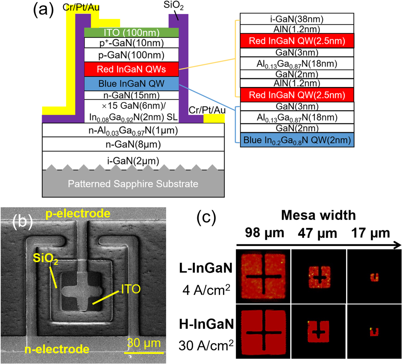
We designed red μLEDs with different mesa dimensions ranging from 98 × 98 to 17 × 17 μm2. 84) The schematic of the μLED structures is shown in Fig. 7(a). The μLED mesas were patterned by standard photolithography and then etched through the ITO and InGaN active region by inductively coupled plasma etching. A wet etching treatment by tetramethylammonium hydroxide (TMAH) was performed for H-InGaN μLEDs to remove the sidewall damage induced by dry etching. The L-InGaN μLEDs did not carry out a chemical treatment. Then, the sidewall was passivated by a SiO2 layer using plasma-enhanced chemical vapor deposition. This SiO2 layer could also serve as an isolated layer between the p-electrode and n-AlGaN. Figure 7(b) shows the top-view SEM image of a typical 47 × 47 μm2 μLED. The n-electrode was extended around the four sidewalls of the μLED, and the p-electrode on ITO was designed as a cross shape. As a result, we could expect uniform current injection into the μLED through the n- and p-electrodes.

Fig. 7. (Color online) (a) Schematic structure of InGaN μLED devices. (b) Top-view SEM image of a 47 × 47 μm2 InGaN μLED. (c) EL emission images of L-InGaN and H-InGaN red μLEDs at 4 and 30 A cm−2, respectively. The mesa width ranges from 98 to 17 μm. (b) is reproduced from Ref. 85 (CC BY 4.0). The L-InGaN data in (c) are reproduced from Ref. 84 with the permission © The Optical Society.
Download figure:
Standard image High-resolution imageWe performed the electrical pumping of red μLEDs at the probe station using a semiconductor parameter analyzer. Figure 7(c) shows the EL emission images of L-InGaN and H-InGaN μLEDs with different mesa lengths from 98 to 17 μm. The L-InGaN and H-InGaN μLEDs were operated at 4 and 30 A cm−2, respectively. Although the In content was quite different in these two kinds of μLEDs, all the μLED chips exhibited uniform red luminescence in most emission areas except for some bright or dark spots at certain positions.
3.2. EL characteristics of InGaN red μLEDs
3.2.1. Fundamental parameters (peak wavelength, FWHM, light output power, and EQE)
The EL characteristics were measured under direct current operation. The picture and cross-sectional schematic of the measurement configuration are shown in Figs. 8(a) and 8(b), respectively. An integrating sphere was located above the sample to collect the light output power and connected through a fiber optic cable to a spectrometer to record the EL spectra. The measurement configuration was called on-wafer testing. 85)

Fig. 8. (Color online) (a) Picture and (b) cross-sectional schematic of the measurement configuration of the on-wafer testing for InGaN μLEDs. (a) is reproduced from Ref. 85 (CC BY 4.0).
Download figure:
Standard image High-resolution imageFigure 9(a) shows the EL spectra of 47 × 47 μm2 L-InGaN and H-InGaN μLEDs at 4 and 30 A cm−2, respectively. The peak wavelengths for L-InGaN and H-InGaN μLEDs were located at 626 and 631 nm, respectively. These peak wavelengths were very close to the primary red emission wavelength (630 nm) defined by Rec. 2020. The FWHMs of L-InGaN and H-InGaN μLEDs were 53 and 60 nm, respectively. The broader FWHM of H-InGaN μLEDs was reasonable because higher-In-content would cause more In fluctuation.

Fig. 9. (Color online) (a) EL spectra of a 47 × 47 μm2 L-InGaN μLED at 4 A cm−2 and a 47 × 47 μm2 H-InGaN μLED at 30 A cm−2. (b) Peak wavelength and (c) FWHM of L-InGaN and H-InGaN μLEDs with a dimension from 98 × 98 to 47 × 47 μm2 at different current densities. (d) Light output power and (e) EQE of L-InGaN and H-InGaN μLEDs with a dimension from 98 × 98 to 47 × 47 μm2 at different current densities by on-wafer testing. (f) Output power density compared to other works. The solid dots are values from μLEDs based on on-wafer testing, and the hollow dots are values from large-size LEDs measured in the integrating sphere.
Download figure:
Standard image High-resolution imageWe then investigated the current density dependences of the peak wavelength and FWHM for InGaN red μLEDs at RT, as shown in Figs. 9(b) and 9(c), respectively. Regardless of the In content in red QWs, the 98 × 98 and 47 × 47 μm2 InGaN μLEDs exhibited the identical behaviors for the peak wavelength and FWHM at different current densities. This phenomenon was similar to the large-size InGaN red LEDs, implying the constant QCSE in red QWs with the chip size shrinking down to 47 × 47 μm2.
Also, the L-InGaN and H-InGaN red μLEDs exhibited a large peak wavelength blue-shift of approximately 35 and 60 nm at 2 to 50 A cm−2, respectively. The blue-shift of H-InGaN μLEDs was higher than that of L-InGaN μLEDs, especially at the low current injection region. This behavior originated from the strong QCSE and band filling effect in high-In-content InGaN red QWs. 28,37) However, AlGaInP red μLEDs usually show a peak wavelength shift within 2 nm at different current densities, implying a stable peak emission compared to InGaN red μLEDs. 86)
In the case of FWHM, the L-InGaN and H-InGaN μLEDs behaved with different current density dependences. At a low current density below 10 A cm−2, the FWHM of H-InGaN μLEDs decreased rapidly with the current density. The total reductions of the FWHMs were in the range of 17–19 nm for 98 × 98 and 47 × 47 μm2 H-InGaN μLEDs from 2 to 10 A cm−2. However, the reduction of the FWHM for L-InGaN μLEDs was only 2 nm from 2 to 10 A cm−2. The much higher reduction amount of the FWHM for H-InGaN red μLEDs originated from many deep localized states in H-InGaN QWs.
At the high current density above 10 A cm−2, the FWHM of H-InGaN μLEDs continued to decrease but within 2 nm up to 50 A cm−2. This implied that the localized states in the H-InGaN QWs still existed but became saturated with increasing current density. In contrast, the FWHMs of L-InGaN μLEDs started to increase slightly. This opposite movement was due to the heat generation in red QWs at the high current densities, which was identical to the FWHM behavior of large-size red LEDs discussed in Sect. 2.2.2.
We measured the average light output power of L-InGaN and H-InGaN μLEDs as a function of the current density by on-wafer testing in Fig. 9(d). Also, we were able to calculate the on-wafer EQEs at different current densities from the measured light output power, as shown in Fig. 9(e). The EQEs of InGaN μLEDs in the dimension from 98 × 98 and 47 × 47 μm2 were quite similar regardless of low- and high-In-contents in red QWs. The EQEs of L-InGaN μLEDs corresponding to red emission at the peak wavelength of 626 nm were within 0.34%–0.36% at 4 A cm−2. Interestingly, the EQEs of H-InGaN μLEDs corresponding to red emission at the peak wavelength of 631 nm were also within 0.34%–0.36% at 30 A cm−2. This meant that the L-InGaN and H-InGaN red μLEDs could achieve similar EQEs regardless of operation at low and high current densities, respectively.
For L-InGaN μLEDs, lower-In-content in red QWs should exhibit a higher EQE. However, the SRH recombination was dominant at the low current density operation, which would lower the EQE of the devices. For H-InGaN μLEDs, the high driven current density was able to saturate most SRH recombination centers, resulting in the improvement of the devices' EQE. Therefore, the different operation current density caused the L-InGaN and H-InGaN μLEDs to exhibit similar EQE in Fig. 9(e).
To compare the on-wafer testing and the measurement in the integrating sphere, we measured the absolute light output power of 47 × 47 μm2 green and amber μLEDs. We defined the calibration factor as the following formula:
This calibration method was used in other works. 83,87) All the μLEDs in our works were not fabricated on die chips and not encapsulated with resin. We used wire bonding for current injection and put the sample inside the integrating sphere for measurements. As a result, we found that the calibration factor was obtained between 1.7 and 2.6 based on Eq. (2). Therefore, the absolute EQE for our red μLEDs was estimated from 0.58 to 0.94%. The estimated results were comparable to 25 × 25 μm2 AlGaInP red μLEDs operated below 30 A cm−2, 86) illustrating the great potential of InGaN material for red μLEDs.
Generally, different applications require different luminance, which finally determines the operated current densities of μLEDs. Luminance was related to the output power density, so we calculated the output power density of L-InGaN and H-InGaN μLEDs at different emission wavelengths. We also presented the other reported data for InGaN large-size LEDs and μLEDs and AlGaInP μLEDs in Fig. 9(f) for comparison. All the data for μLEDs were estimated by on-wafer testing, while the data for large-size LEDs were obtained by measurements in the integrating sphere. The H-InGaN μLEDs that were operated at high current density could achieve a higher output power density than that of the L-InGaN μLEDs with the same emission wavelength. Also, the output power density of 20 × 20 μm2 AlGaInP red μLEDs was approximately 0.5 mW mm−2 at 30 A cm−2 (measured by on-wafer testing with substrates). At a similar emission wavelength, the output power density of H-InGaN μLEDs was 2 mW cm−2 at 30 A cm−2, which was almost 4 fold that of AlGaInP μLEDs. 88) Although the output power density of AlGaInP μLEDs was obtained with the substrates, this comparison illustrated that the InGaN materials had great potential for high-brightness red μLED applications.
3.2.2. Temperature stability of red μLEDs
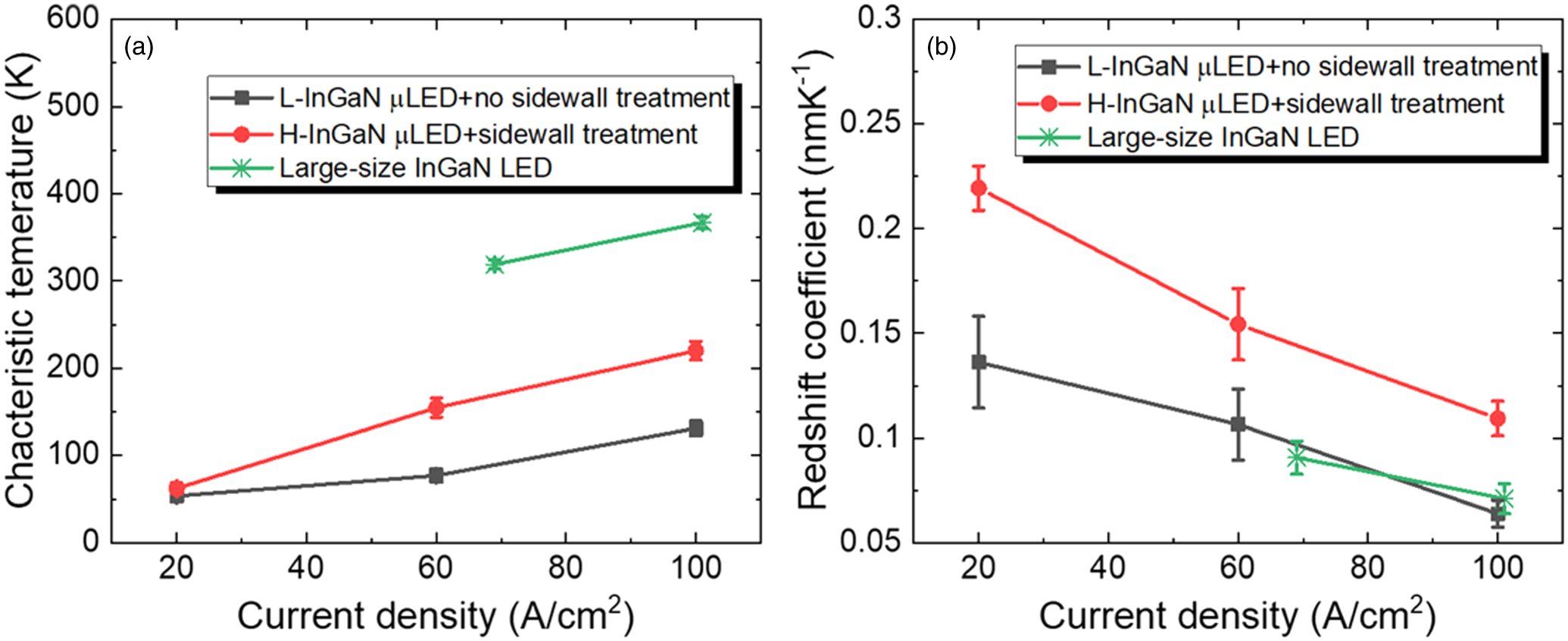
We also measured the temperature dependences of the L-InGaN and H-InGaN μLEDs by adjusting the stage temperature from 295 to 373 K. The characteristic temperatures were obtained by using Eq. (1), as shown in Fig. 10(a). As we discussed large-size LEDs in Sect. 2.2.3, the characteristic temperature was related mainly to the SRH recombination. Because the SRH recombination would be saturated at high current densities, the characteristic temperatures of both L-InGaN and H-InGaN μLEDs were increased by increasing the current density. Meanwhile, the sidewall treatment by TMAH could effectively remove some of the SRH recombination centers at the sidewalls induced by dry etching. 77) Therefore, the characteristic temperature of the H-InGaN μLED was higher than that of the L-InGaN μLED. However, the InGaN μLEDs still exhibited lower characteristic temperatures compared to the large-size LEDs, implying that the SRH recombination centers still existed at the surface of the sidewalls of μLEDs.

Fig. 10. (Color online) (a) Characteristic temperature and (b) Red-shift coefficient of the L-InGaN and H-InGaN red μLEDs at different current densities. The results for large-size InGaN LEDs were also plotted for comparison. The stage temperature was varied from 295 to 373 K.
Download figure:
Standard image High-resolution imageThe peak wavelengths of the InGaN μLEDs would also have red-shift with increasing temperature. Thus, we could calculate the red-shift coefficients at different current densities in Fig. 10(b). The red-shift coefficients decreased as the current density increased. This behavior is similar to those of the large-size InGaN LEDs, and we explained the reason in the above discussion. The red-shift coefficients of the H-InGaN μLEDs were larger than those of the L-InGaN μLEDs. The reason for this phenomenon was not clear yet. We believe that the higher defect densities in the H-InGaN red μLEDs will cause inefficient carrier injection into QWs because of more leakage currents through the defects. Thus, the inefficient current injection into the H-InGaN μLEDs would cause higher red-shift coefficients.
3.2.3. Analysis of color coordinates in CIE diagrams
The color coordinates in the color space are important parameters for μLED displays because they determine the physiologically perceived colors in human color vision. Here, we plotted the color coordinates of the L-InGaN and H-InGaN μLEDs in both CIE 1931 and 1976 diagrams [Figs. 11(a) and 11(b)]. The operated current density was 2, 10, 20, and 50 A cm−2 for L-InGaN μLEDs and 10, 20, 30, and 50 A cm−2 for H-InGaN μLEDs. The primary red color according to Rec. 2020 is located at the coordinates of (0.708, 0.292) in CIE 1931 and (0.557, 0.517) in CIE 1976. These coordinates were marked as a red star in the CIE 1931 and 1976 diagrams, respectively.

Fig. 11. (Color online) (a) CIE 1931 and (b) CIE 1976 diagrams of the L-InGaN and H-InGaN red μLEDs. The operated current density is 2, 4, 10, and 50 A cm−2 for the L-InGaN μLEDs (black squares) and 10, 20, 30, and 50 A cm−2 for the H-InGaN μLEDs (green circles). The red stars are the primary red color defined by Rec. 2020.
Download figure:
Standard image High-resolution image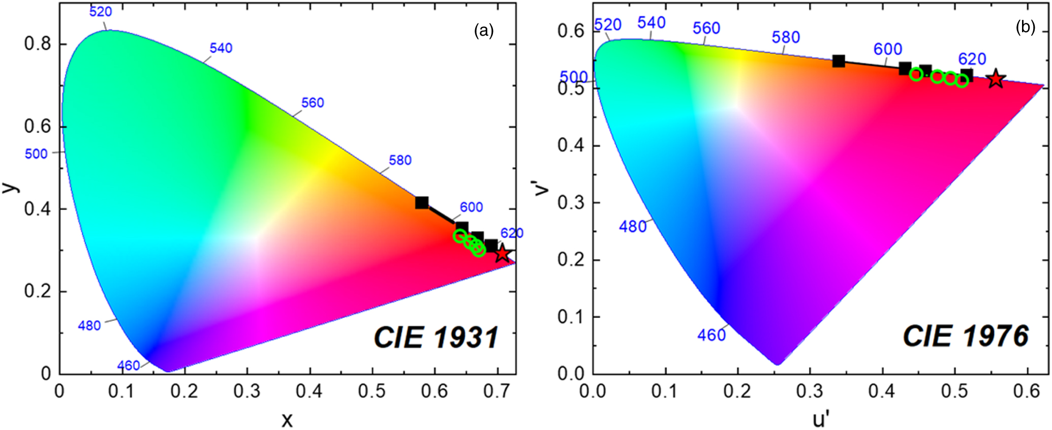
Clearly, at the beginning, the color coordinates of both L-InGaN and H-InGaN μLEDs were very close to the reference point of red color defined by Rec. 2020. However, the locations would move farther away from the reference point as the current densities increased in the CIE 1931 or 1976 diagrams. This movement caused the color variation and also reduced the color gamut area coverage, which are unfavorable features for micro-displays. The shifted distance for the H-InGaN μLEDs was much smaller than that of the L-InGaN μLEDs, demonstrating better color stability for the H-InGaN μLEDs than for the L-InGaN μLEDs. However, the color positions of H-InGaN μLEDs were not like those of the L-InGaN μLEDs at the edge of the color space in the CIE 1931 or 1976 diagrams. This gap illustrated that the color saturation for the H-InGaN μLEDs was insufficient, which was due to the broad FWHM of the H-InGaN μLEDs.
Because the peak wavelength has a very small shift at different current densities, 86) the position in the CIE diagram was expected to remain almost constant when the AlGaInP μLEDs were driven at different current densities, demonstrating good color stability for the AlGaInP red μLEDs. Therefore, to replace AlGaInP red μLEDs in μLED displays, InGaN red μLEDs required further improvements in the aspect of color stability.
4. Conclusion and prospect
In this review, we present an overview of our recent progress on InGaN-based red LEDs on c-plane sapphire substrates. Both the large-size LEDs and μLEDs including their structures and optical performance were investigated carefully. Our best bare InGaN LEDs exhibited an EQE and WPE of 1.6% and 1.0% at the peak wavelength of 633 nm at 20 mA, respectively. Also, the red μLEDs that were operated at low and high current densities had similar on-wafer EQEs of 0.34%–0.36% (estimated as 0.58%–0.94% of absolute EQE) for the emission wavelength around 630 nm. The CIE coordinates of our red μLEDs could approach the primary red color point defined by Rec. 2020, demonstrating the possibility of the wide color gamut coverage using InGaN red μLEDs.
From the perspective view, InGaN red LEDs from the large-size to μLEDs are an important research field for extending the applications of III-nitride optoelectronic devices in the visible wavelength range. Especially driven by μLEDs for high-resolution display, InGaN red μLEDs will play a critical role in the full-color μLED displays based on nitride semiconductor materials. The main issue for current InGaN red large-size LEDs and μLEDs is the crystal quality of InGaN red QWs, which finally determines the efficiency of the LED devices. Another important issue is the large blue-shift at different current densities, which influences the color stability of InGaN red LEDs, especially for μLEDs. Regardless of the big performance gap between large-size InGaN and AlGaInP red LEDs, the EQE and temperature stability of InGaN red μLEDs is expected to be superior to that of AlGaInP μLEDs, especially when the dimension shrinks down to less than 25 μm. This great potential may attract more academic researchers and industrial companies to enter this field and push InGaN red μLEDs to be commercialized in the near future.
Acknowledgments
This work is supported by King Abdullah University of Science and Technology (KAUST) (BAS/1/1676-01-01).