
Abstract
We investigated the adhesion strength of Cu films grown using chemical vapor deposition (CVD) on a Co(W) layer, which was grown using atomic layer deposition (ALD), for Cu interconnect applications in ultra-large scale integration (ULSI). Co(W) forms an effective barrier to the diffusion of Cu and forms an adhesion layer in a single barrier. Amidinato precursors were used in the deposition of Co and W, which contain neither O nor F, and yielded high-purity Co(W) films. Furthermore, the use of an amidinato Cu precursor was also found to be important in enabling Cu deposition without interfacial contamination. The W content of the Co(W) layer was optimized to 14 at% via an evaluation of the diffusion barrier properties, the electrical conductivity, and the adhesion strength with the Cu layer. A CVD-Cu/ALD-Co(W) stack was formed using amidinato precursors for the growth of both films, and was found to exhibit favorable properties compared with a conventional PVD-Cu/PVD-Ta/TaN stack. It was also favorable to a PVD-Cu/PVD-Ru/TaN stack in terms of the diffusion barrier properties and electrical conductivity, with a similar adhesion strength for Cu. For these reasons, our Co(W) films have potential applications in reliable and high-performance Cu interconnects in next-generation ULSI.
Export citation and abstract BibTeX RIS
The dimensions of complementary metal oxide semiconductor (CMOS) transistors in ultra-large scale integration (ULSI) have scaled considerably over the past few decades, which has led to continued improvements in performance and reductions in costs. The typical feature size of Cu interconnects in ULSI has also scaled for the same reasons.1 Currently, Cu interconnects are fabricated using the so-called "damascene process," which consists of four deposition steps: sputtering of a Cu diffusion barrier layer onto the interlayer dielectric (ILD), sputtering of an adhesion-promoting layer (or liner layer) onto the barrier layer, sputtering of a Cu seed layer, and subsequent electroplating of Cu. The excess Cu is then removed using chemical mechanical polishing (CMP). A Ta/TaN double layer is currently used as a liner/barrier system.2–4
Scaling the Cu feature size, however, introduces two major reliability issues: electromigration (EM) and stress-induced voiding (SIV). These issues result from the increased current density within the Cu line, as well as the resulting internal stresses. Failures may result from insufficient adhesion strength between the liner layer (currently Ta) and the Cu seed layer, as well as internal stresses within the Cu seed layer.5,6 For this reason, the replacement of Ta with materials that have higher adhesion strength with Cu is desirable. Recently, Ru7–14 and Co15–19 have received attention for applications as liner layers because these elements can result in an increased EM life-time. The improved performance is attributed to a high adhesion strength with the Cu, which results from the close match in lattice constants and similar crystal structures (hexagonal close packed (hcp) or face centered cubic (fcc)), compared with Cu (fcc), whereas Ta has a body centered cubic (bcc) structure.9,13 Co has some advantages compared with Ru, including lower cost and better compatibility with the CMP process.20–23 Although Co itself does not exhibit barrier properties, we have previously shown that a Co film containing 14 at% W; i.e., a Co(W) film, exhibited excellent Cu diffusion barrier performance by forming a grain-boundary stuffing structure, while maintaining the high conductivity that is inherent of Co.24–28 Favorable adhesion of Co(W) with Cu is also expected because it mainly consists of Co. Dissolution of Co into Cu is a well-known problem with Co liner layers;18 however, this was suppressed with the Cu/Co(W) system. Thus, Co(W) has potential applications as a single-layer liner and barrier. Single-layer Co(W) also helps to increase the total line conductance, which decreases as the dimensions of the interconnect line scale, because the transition from a double-layer (Ta/TaN) to a single-layer (Co(W)) provides greater volume for Cu due to the reduced total thickness of the liner and barrier. The adhesion of the barrier layer onto underlying ILD is another issue for Cu interconnects, and sufficient adhesion of Co(W) to SiO2 has been demonstrated.28
The relation between the fabrication method of Cu/Co(W) and the properties of the resulting film are discussed below. Because Cu/Co(W) is aimed at the 1x (10–18) nm-node, which requires conformal step coverage on high-aspect-ratio and extremely narrow features, Co(W) and Cu should be grown using a deposition method that can provide good step coverage; i.e., not using physical vapor deposition (PVD) methods such as sputtering. We therefore used atomic layer deposition (ALD) for Co(W) and chemical vapor deposition (CVD) for Cu. This is because Co(W) requires atomic scale control over the thickness, as well as good film-uniformity, in addition to step coverage. ALD-Cu suffers from film-agglomeration during the initial stages of growth, and thereby CVD is more suitable for deposition of the Cu film. Favorable step coverage on high-aspect-ratio trenches has been demonstrated for Co(W)-ALD26,28 and Cu-CVD.29 We have previously shown that the barrier properties and the conductivity of ALD-Co(W) depend strongly on the precursors used during deposition.26,30 Co(W) grown using carbonyl precursors was shown to be inferior to TaN in terms of the diffusion barrier properties.25,30 This was explained by the incorporation of oxygen in the film during deposition of Co(W), which resulted from ligands of the carbonyl precursors. In contrast, oxygen-free precursors (metallocene or amidinato compounds) enabled deposition of Co(W) without the incorporation of O.24,26,30 As a result, metallocene- or amidinato-based Co(W) films exhibited higher conductivity and even superior barrier performance compared with PVD-TaN or carbonyl-based films.24,26,27,30
Co(W) grown using ALD has also been characterized in terms of the adhesion strength of CVD-Cu.31 The procedure was same with this work, as will be described in the following section. The adhesion strength of the CVD-Cu layer on the ALD-Co(W) grown using carbonyl precursors with was significantly lower than that of the PVD-Cu/PVD-Ru system,9,13,31 which is a major contender for next-generation ULSI Cu interconnects; it was, however, higher than that of the PVD-Cu/PVD-Ta system,31,32 which is a current de facto standard material. This may be due to partial oxidation of the Co(W) layer during deposition. Our current goal is to enhance the adhesion strength of the ALD-Co(W) and CVD-Cu layers so that it is comparable to that of PVD-Ru and PVD-Cu, which may be achievable by engineering the surface and interface chemistry during deposition of both the ALD-Co(W) and CVD-Cu layers.
In this study, we attempted to increase the adhesion strength between the CVD-Cu and ALD-Co(W) layers by preventing surface contamination of the Co(W) layer. First, we assessed the impact of the use of the oxygen-free Co and W precursors (metallocene and amidinato33) on the adhesion strength between the ALD-Co(W) and CVD-Cu layers, followed by a comparison with previously reported growth using O-containing precursors (carbonyl). As a result, we altered the choice of Cu precursor for CVD because of contamination caused by the Cu precursor ligand, which was found at the Cu/Co(W) interface, and which degraded the adhesion properties. We used the O- and F-free amidinato Cu precursor33 for the Cu-CVD layers, and achieved an uncontaminated Cu/Co(W) interface. We then evaluated the adhesion strength between the ALD-Co(W) and CVD-Cu layer, where amidinato precursors were used in the deposition of both films. The adhesion strength was subsequently optimized by varying the W content, as the W content affects the barrier properties and the conductivity of the Co(W).27,30 We then summarize the results for the CVD-Cu/ALD-Co(W) system, and compare these with data for PVD-Cu/PVD-Ru and PVD-Cu/PVD-Ta.31
Evaluation of the Adhesion Strength
In this section we discuss the adhesion strength of a Cu grain on an underlayer. A methodology to evaluate the adhesion strength between a Cu film and an underlayer is described, which is based on wetting angles of the Cu grains on the underlayer. The shape of Cu grains in thermodynamic equilibrium is determined by the balance of four forces, as shown in Fig. 1. Force balance in the horizontal direction is given by Young's equation; i.e.,
![Equation ([1])](https://content.cld.iop.org/journals/2162-8777/4/2/P20/revision1/jss_4_2_P20eqn1.jpg)
where θ is the wetting angle of the Cu grains, FCu is the surface tension of Cu, Fund is the surface tension of the underlayer, and Fint is the interfacial tension. Because of the equivalence between the forces and the surface or interfacial energies, Equation 1 can be rewritten as follows:34
![Equation ([2])](https://content.cld.iop.org/journals/2162-8777/4/2/P20/revision1/jss_4_2_P20eqn2.jpg)
where γCu is the surface energy of Cu, γund is the surface energy of the underlayer, and γint is the interfacial energy between the Cu and the underlayer. The work of adhesion between Cu and the underlayer, Wad, is defined by Dupré's equation;35 i.e.,
![Equation ([3])](https://content.cld.iop.org/journals/2162-8777/4/2/P20/revision1/jss_4_2_P20eqn3.jpg)
Equations 2 and 3 can be combined as follows:
![Equation ([4])](https://content.cld.iop.org/journals/2162-8777/4/2/P20/revision1/jss_4_2_P20eqn4.jpg)
The adhesion strength of Cu with the underlayer is therefore a function of the wetting angle of Cu grains formed on the underlayer (Young–Dupré equation).
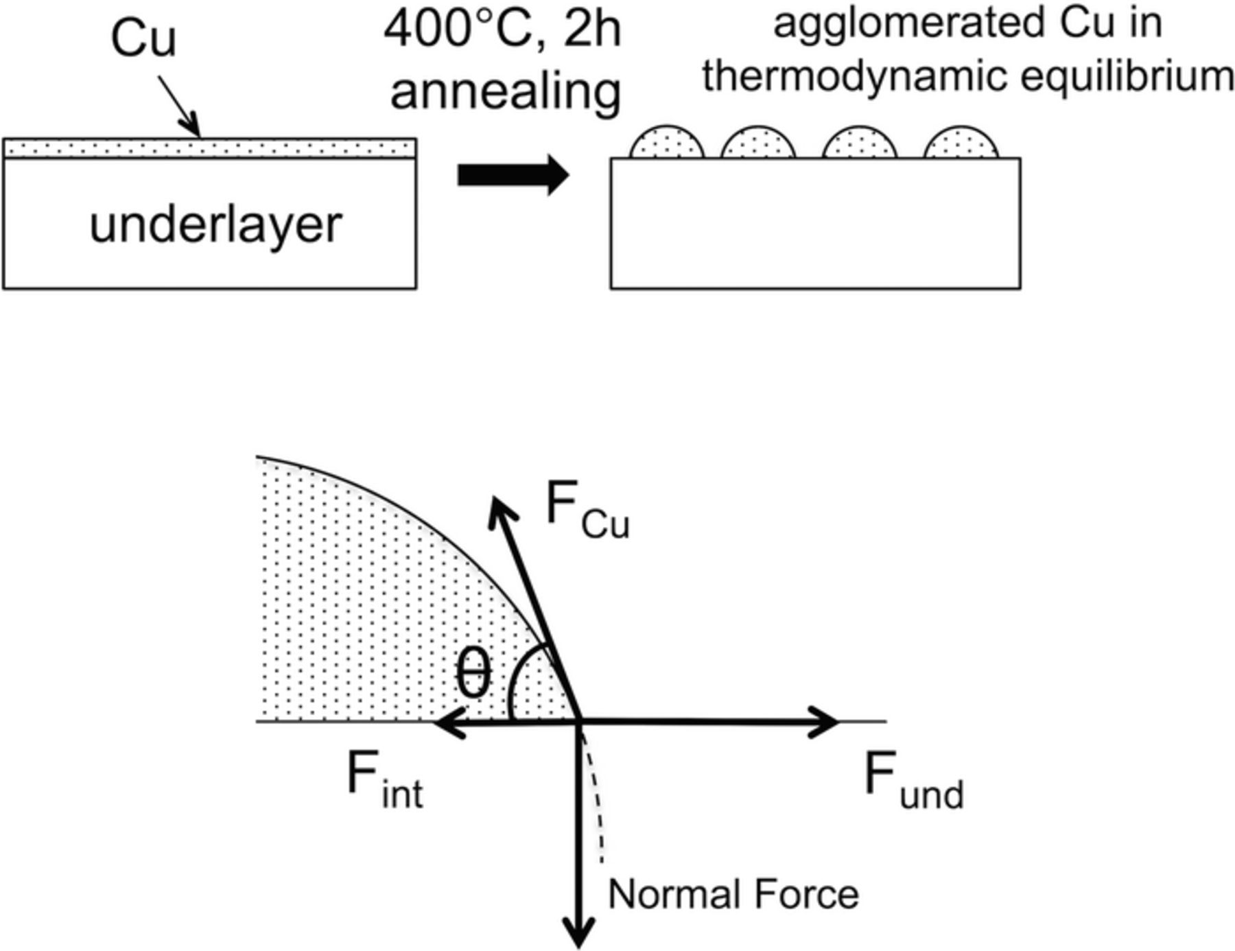
Figure 1. Schematic diagrams showing side-views of the agglomerated Cu grains after post-annealing and the force balance.
In this study, continuous 20-nm-thick Cu films were formed on the Co(W) underlayers, followed by thermal annealing to allow agglomeration of the Cu film, until thermodynamic equilibrium was reached, whereby the internal stresses in the Cu film are released. In this manner, the intrinsic adhesion strength between the Cu and the Co(W) underlayer could be evaluated quantitatively, and was not disturbed by internal stresses or defects in the Cu film. This methodology is feasible due to the relatively low melting point of Cu (1085°C). In addition, with the ALD-Co(W) underlayer, the Cu adhesion strength on a flat substrate is also applicable to that within a trench; it has previously been shown that ALD-Co(W) films grown in a high-aspect-ratio trench exhibit uniform thickness and a homogeneous W composition on the trench sidewalls,26 which indicates that the adhesion of Cu onto the side wall or bottom of the trench should be the same as on flat surface.
As described above, the adhesion strength of a Cu film on an underlayer can be assessed from the wetting angle of Cu grains formed via agglomeration of the Cu film. This methodology has become increasingly common with Cu interconnects for ULSI applications.9,13,31,32,36–38 Note that this methodology has been verified experimentally;39–43 for example, Meuler et al. obtained the same adhesion strength using two distinct methods in an ice/metal system, that is, mechanical measurements of the shear stress and wetting angle measurements of water droplets.42 This methodology has been employed in many materials systems, including ice/metal,42 ice/polymer,41,42,44–46 polymer/polymer,43 polymer/ceramic,44 metal/ ceramic37,47 and ceramic/ceramic.39,40,48
Experimental
Variation of the sample structures
In this study, six types of stacked sample were compared, as listed below and shown in Fig. 2. Samples (a) and (e) are shown for comparison, and data were taken form Ref. 31. The substrate for samples (a)–(d) was a Si with an SiO2 coating formed via thermal oxidation; sample (e) was an Si substrate with an SiO2 coating formed using plasma-enhanced CVD with a tetraethoxysilane (TEOS) precursor; and sample (f) was grown directly on an Si substrate.
- (a)CVD-Cu (β-diketonato)/ALD-Co(W) (carbonyl)31
- (b)CVD-Cu (β-diketonato)/ALD-Co(W) (metallocene)
- (c)CVD-Cu (β-diketonato)/ALD-Co(W) (amidinato)
- (d)CVD-Cu (amidinato)/ALD-Co(W) (amitinado)
- (e)PVD-Cu/PVD-Ta/PVD-TaN31
- (f)PVD-Cu/PVD-Ru
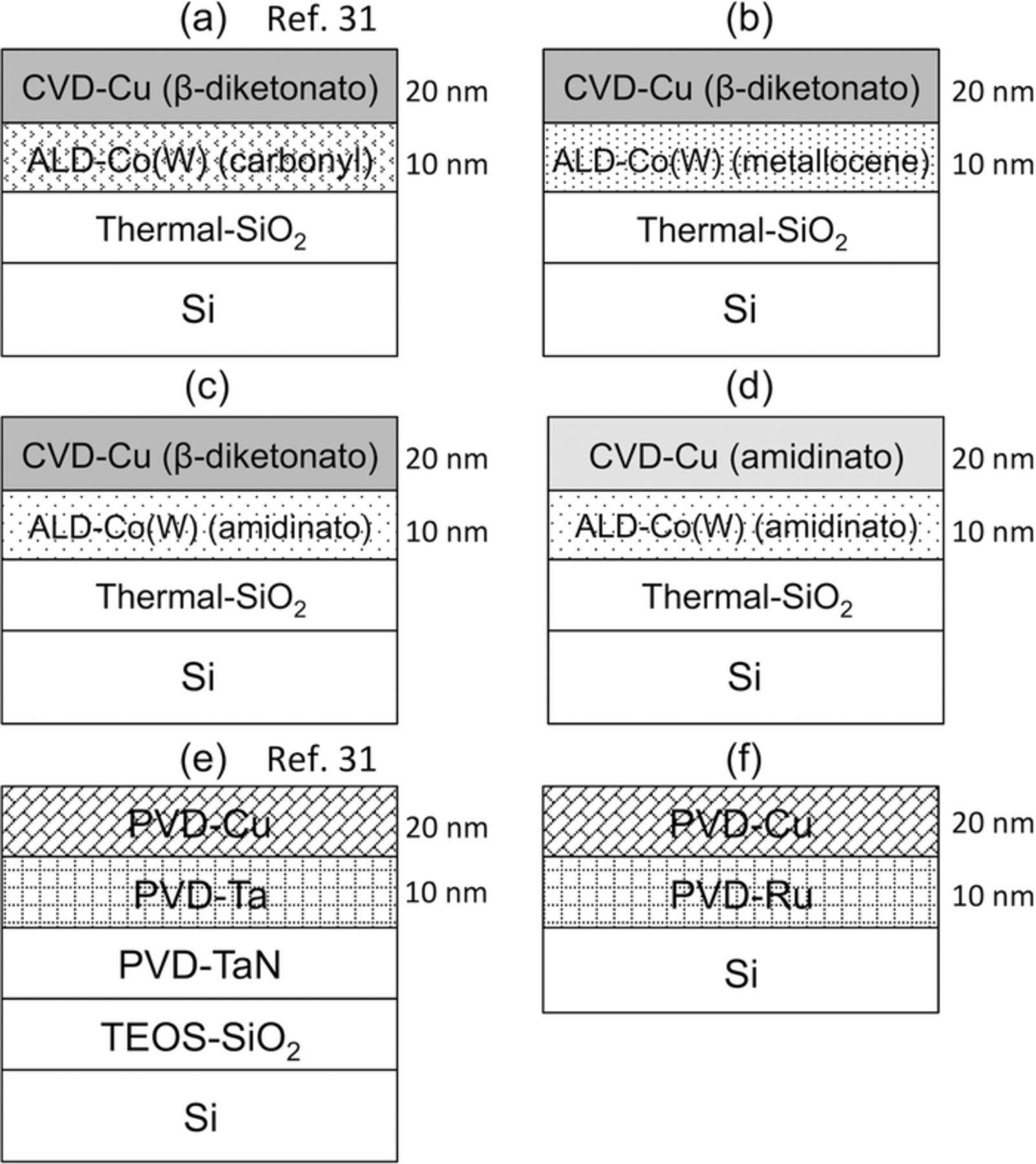
Figure 2. Schematic diagrams showing side-views of the CVD-Cu/ALD-Co(W), PVD-Cu/PVD-Ta, and PVD-Cu/PVD-Ru samples.
ALD deposition of the Co(W) underlayer
Deposition of Co(W) was carried out using a shower-head-type cold-wall ALD chamber. The base pressure of the ALD chamber was maintained at 1 × 10⁻⁵ Pa using a turbo molecular pump. The metallocene precursors bis(cyclopentadienyl)cobalt ((C5H5)2Co) and bis(cyclopentadienyl)dihydridotungsten ((C5H5)2WH2) were used, as shown in Fig. 3B, and NH2 radicals were formed by cracking NH3 using a hot-wire for use as a reducing agent. This set-up is termed hot-wire-assisted atomic layer deposition (HW-ALD). Deposition was carried out with a substrate temperature of 350°C and a total pressure of 27 Pa. The other growth conditions were as described in Refs. 24 and 49.
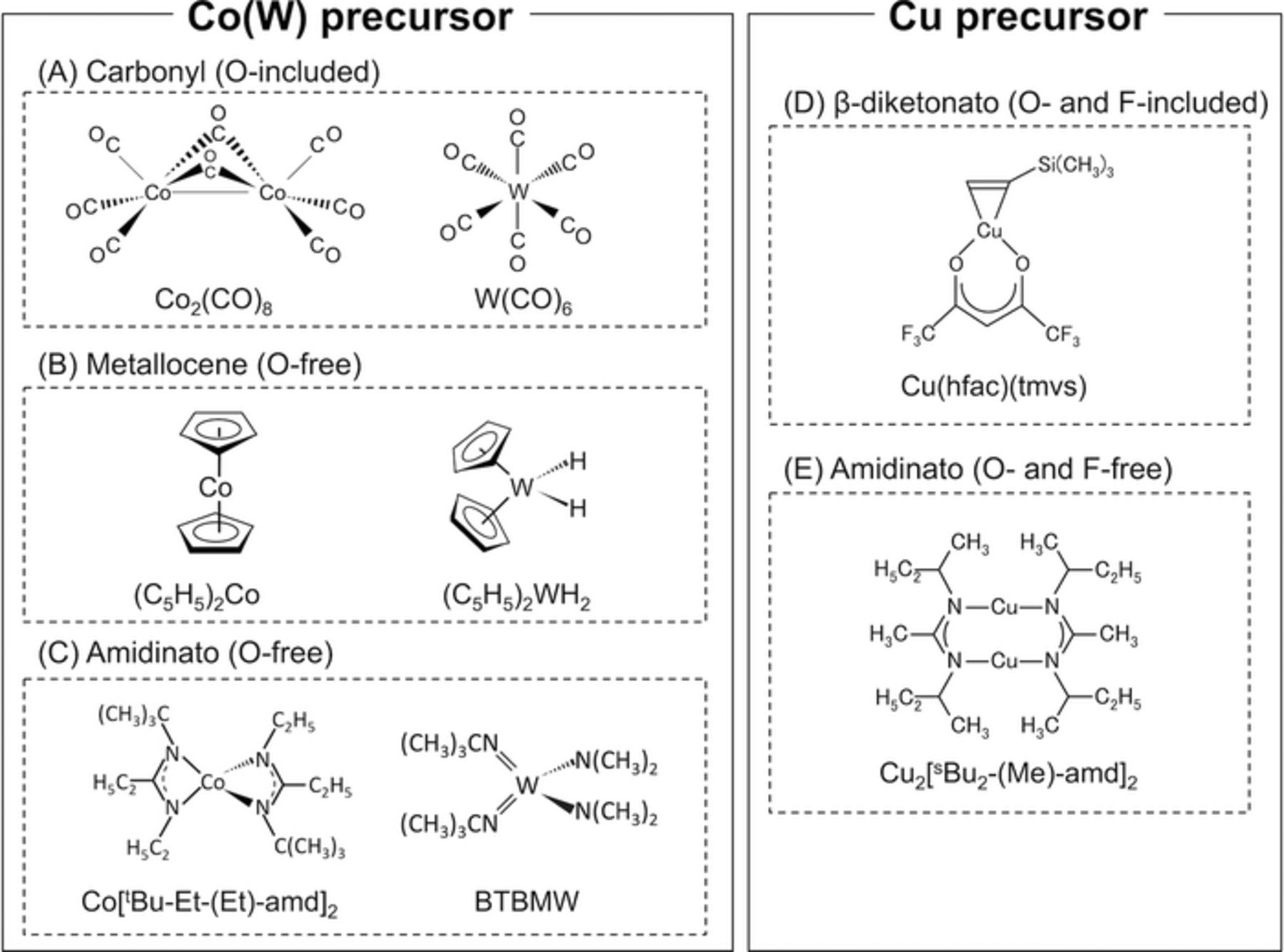
Figure 3. Structural diagrams of the Co and W precursors used for Co(W)-ALD and the Cu precursors used for Cu-CVD in this work.
The amidinato precursors bis(N-tert-butyl-N'-ethyl-propaneamidinato)cobalt(II) [Co[tert-Bu-Et-(Et)-amd]2] and bis(tert-butylimido)-bis(dimethylamino)tungsten(IV) [BTBMW] were used, as shown in Fig. 3C, with NH3 as a reducing agent. Deposition was carried out at a substrate temperature of 375°C and a total pressure of 40 Pa. Further details can be found in Refs. 26 and 27.
With both the amidinato and metallocene precursors, the supply sequence was Co-precursor/NH3/W-precursor/NH3, and deposition was completed with the NH3 supply continued after the Co precursor supply had been terminated. This completion strategy provided a Co-rich surface, which is favorable for a high adhesion strength with Cu.31 The Co(W) underlayers were 10-nm-thick in all cases. The W content was varied in the range 7–31 at% by controlling the feed time or partial pressure of the W precursor.
The film composition was measured using X-ray photoelectron spectroscopy (XPS) (ULVAC PHI 1600C), which had an accuracy of within 1%. The XPS measurements were carried out before and after a 3-nm-deep etch, which was carried out using an Ar ion gun in order to examine the elemental compositions of the surface and the inside of the film.
CVD deposition of Cu
Cu films were formed using a shower-head-type cold-wall CVD chamber, and using β-diketonato and amidinato precursors. The chamber used for Cu deposition was connected to that used for Co(W) deposition via load-lock chamber, as shown in Fig. 4, enabling transfer of the specimens without contamination with air. The β-diketonato precursor was copper(I) hexafluoroacetylacetonato trimethylvinylsilane [Cu(hfac)(tmvs) or Cupra-Select]50,51 (see Fig. 3D); the amidinato precursor was copper(I) (N,N'-di-sec-butylacetamidinato) dimer [Cu2[sec-Bu2-(Me)-amd]2]29,52,53 (see Fig. 3E). Cu(hfac)(tmvs) is the most commonly used Cu precursor for CVD, and was used in our previous work;31 the ligands of Cu(hfac)(tmvs) consist of C, F, and O atoms. Cu2[sec-Bu2-(Me)-amd]2 is a recently developed growth precursor, the ligands of which consist of C and N. H2 (>99.99999%) was used as a reducing agent, and He (>99.99995%) was used as a carrier gas. These were supplied to the equipment following purification using Agilent Technologies combination gas traps to eliminate moisture. The deposition temperature for the β-diketonato precursor was 150°C, and that for the amidinato precursor was 200°C. The total pressure in the chamber during deposition was 665 Pa. The base pressure of the Cu-CVD chamber was maintained at 1 × 10⁻⁴ Pa using a turbo molecular pump. When the precursor was altered, the equipment was baked at 150°C for 2 days to remove any precursor adsorbed onto the inner surface of the chamber and the feed lines. The CVD-Cu films were 20-nm-thick in all cases. The film composition was measured using XPS with the same procedure as for the Co(W) measurement.
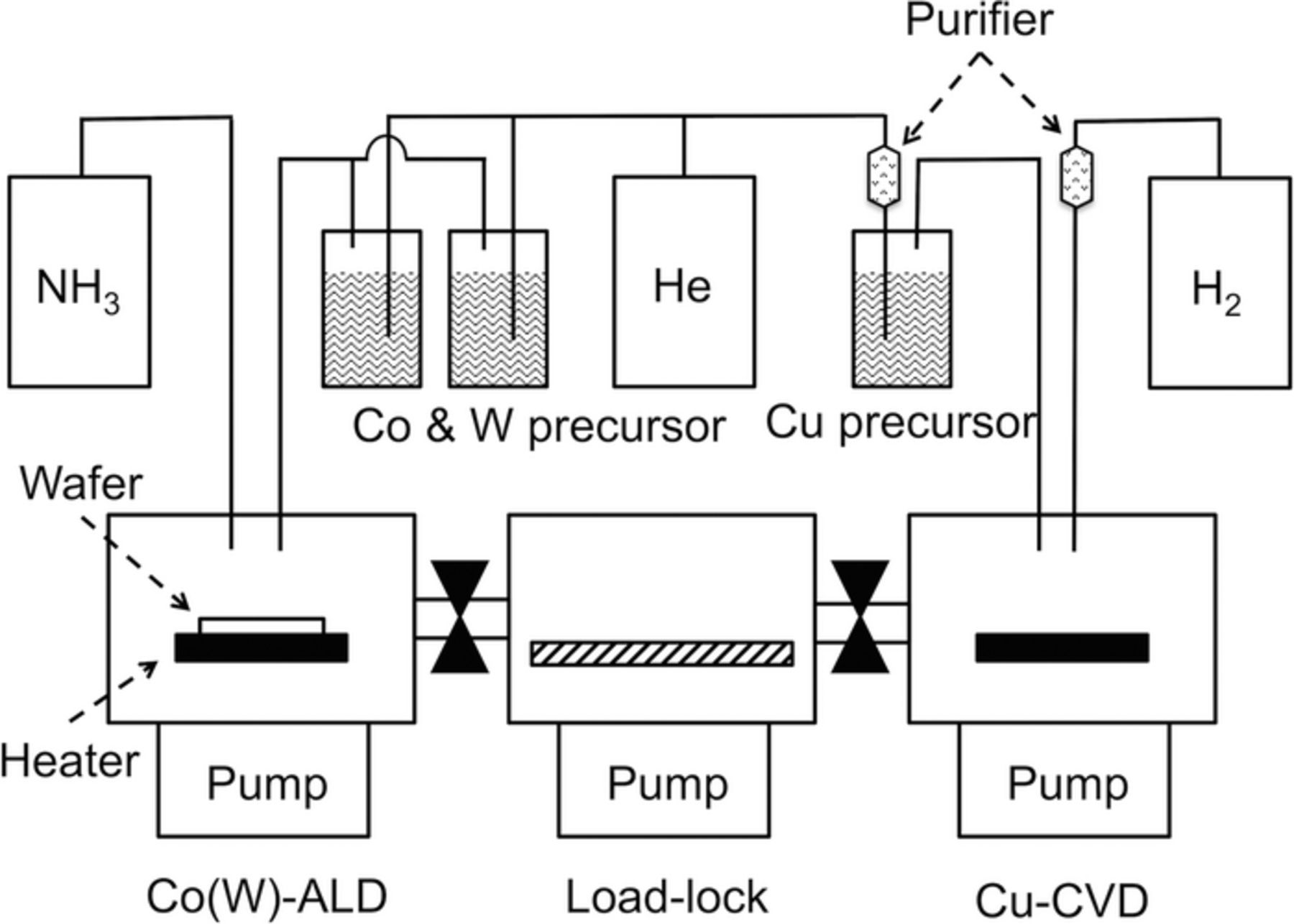
Figure 4. Schematic diagrams showing side-views of the Co(W)-ALD and Cu-CVD systems.
Cu agglomeration via annealing
Annealing was carried out following Cu deposition to allow the continuous Cu film to agglomerate to form Cu grains using an annealing furnace, which was separated from the deposition chambers. The base pressure of the furnace was 2 × 10⁻⁵ Pa, and the sample was annealed at 400°C for 2 hours at 6650 Pa in an H2 atmosphere (>99.99999%). The annealing condition (400°C and 2 hours) was carefully optimized in order to obtain the shape of Cu grains in thermodynamic equilibrium, which is free from internal stresses or facet developments on surface.
Analysis
The adhesion strength between the Co(W) and Cu layers was evaluated by means of the wetting angle. 15 agglomerated Cu grains were chosen from the substrate. Side-views of these grains were then imaged using a field-emission scanning electron microscope (FE-SEM) (Hitachi S-5000H). The wetting angles at both sides of the 15 Cu grains were measured, giving 30 wetting angles. These results were plotted as a cumulative probability distribution. Note that 30 measurements are statistically sufficient because the distribution of the results and average wetting angle were same within the range ±1° even if the measurement point was increased up to 60. The difference between the average wetting angle and the 50% probability angle were also within a range of ±1° for all samples. The gradients of the distributions did not exhibit significant differences. Hence, in the results section, average wetting angles are used to determine the Cu adhesion energy. A difference of more than 5° in the wetting angles is considered a significant difference.
To evaluate the effect of oxidation of the Co surface on the adhesion strength between the Co and Cu layers, the agglomeration tolerance of the continuous Cu film was used as an index, rather than the wetting angle. Thermal annealing at 400°C could not be used to allow agglomeration of the continuous Cu film, as this also facilitated inter-diffusion of Cu and Co. Instead, the Cu film was annealed at 180°C for 2 h in an H2 environment (>99.99999%). The resulting surface coverage of Cu was then measured using XPS, whereby a surface coverage of 100% denotes strong adhesion, and a value <100% indicates weak adhesion. Two types of Cu/Co stack were fabricated using radio frequency (RF) sputtering (ULVAC VTR-150M/SRF) on thermally grown SiO2/Si substrates; i.e., PVD-Cu/PVD-Co and PVD-Cu/PVD-CoOx, where the former was formed continuously in the PVD chamber and thus contamination did not occur at the Cu/Co interface, whereas the latter was exposed to air following Co film deposition for 1 minute to form a native oxide layer at the Co surface. The PVD-Co film was 20-nm-thick and the PVD-Cu films were 5-nm-thick.
To characterize contamination at the CVD-Cu/ALD-Co(W) interface, as well as the chemical state of the Co(W) surface, post-growth thermal annealing was carried out, followed by wetting angle measurements, in which the overlying Cu film was agglomerated to reveal the Co(W) surface. It was then analyzed using XPS, where the obtained data include information on the Cu grain surface as well as the surface of the Co(W) underlayer.
Results and Discussion
The measured Cu wetting angles are listed in Table I. Using these results, in this section we discuss the adhesion strength between the CVD-Cu layer and the ALD-Co(W) layer. Because the adhesion strength is affected by the presence of impurities at the Cu/Co(W) interface, as well as the W content of Co(W) film, we investigated the optimal precursors for both the Co(W)-ALD and Cu-CVD layer to form an uncontaminated Cu/Co(W) interface. As we reported previously,31 CVD-Co(W) exhibits larger Cu wetting angles (i.e., poorer Cu adhesion strength) than ALD-Co(W), which is attributed to the large W content present at the Co(W) surface; for this reason, CVD-Co(W) layers are not investigated further. When the β-diketonato Cu precursor was used with Cu-CVD, the Cu wetting angle on ALD-Co(W) was constant in the range 57–60° and showed no significant dependency on the Co(W)-ALD precursors nor the W content. These Cu wetting angles were significantly larger than that of the PVD-Cu/PVD-Ru stack (42°). The β-diketonato Cu precursor resulted in O- and F-contamination on the Co(W) underlayers in the initial stages of the Cu growth. In contrast, when the amidinato Cu precursor was used for the Cu-CVD growth, the Cu wetting angle increased significantly (48°) due to the elimination of O and F impurities at the Cu/Co(W) interface. The W content in the Co(W) film was then optimized. The use of the amidinato precursors for both the Co(W)-ALD and subsequent Cu-CVD resulted in a Cu/Co(W) interface that contained neither O nor F impurities. The W content in Co(W) films was found to significantly affect the Cu adhesion strength. A smaller W content resulted in a smaller Cu wetting angle (i.e., a higher Cu adhesion strength). Considering the three desirable properties; i.e., an effective Cu diffusion barrier, a large electrical conductivity, and a high adhesion strength with Cu, we find that a W content of 14 at% provided optimal Co(W) film properties. This optimized CVD-Cu/ALD-Co(W) stack was compared with a PVD-Cu/PVD-Ta stack (which is the de facto standard) as well as a PVD-Cu/PVD-Ru (a major contender for next-generation ULSI Cu interconnects).
Table I. A summary of the average wetting angles of the agglomerated Cu grains on various underlayers.
| [degree] | ||||||
|---|---|---|---|---|---|---|
| Cu growth method | ||||||
| CVD-Cu | ||||||
| W at% | PVD-Cu | β-diketonato | Amidinato | |||
| Underlayer | CVD-Co(W) | 7 | Carbonyl | - | 6131 | - |
| 14 | - | 6931 | - | |||
| ALD-Co(W) | 7 | Carbonyl | - | 5731 | - | |
| 14 | - | 5931 | - | |||
| 7 | Metallocene | - | 59 | - | ||
| 7 | Amidinato | - | - | 43 | ||
| 16 | - | 60 | 48 | |||
| 23 | - | - | 58 | |||
| 31 | - | - | 70 | |||
| PVD-Ta | 7731 | - | - | |||
| PVD-Ru | 42 | 41 | 43 | |||
Effects of the Co(W)-ALD precursors on the adhesion strength
In this section, we investigate the effects of the choice of ALD-Co(W) precursors on the adhesion strength of the Cu/Co(W). Fig. 2a shows the structure of the CVD-Cu (β-diketonato)/ALD-Co(W) [W: 7 or 14 at%] (carbonyl),31 Fig. 2b shows the structure of the CVD-Cu (β-diketonato)/ALD-Co(W) [W: 7 at%] (metallocene), and Fig. 2c shows the structure of the CVD-Cu (β-diketonato)/ALD-Co(W) [W: 14 at%] (amidinato). The Cu precursor was β-diketonato for all samples. Prior to evaluating the adhesion strength, the composition of the ALD-Co(W) film was analyzed. A summary of this analysis is listed in Table II. The use of the metallocene and amidinato precursors eliminated the incorporation of O into the Co(W) film (the O content was below the XPS detection limit of <0.1 at%), whereas the use of the carbonyl precursors resulted in incorporation of O at 3–5 at% depending on the W content. The use of oxygen-free precursors eliminated the O in the Co(W) films, as expected. The adhesion strength of the Co(W)/Cu interface of these samples was evaluated. Representative side-views of the Cu grains formed via agglomeration of the continuous Cu film on the ALD-Co(W) underlayers are shown in Fig. 5, and the corresponding wetting angles are plotted in Fig. 6. Contrary to our expectations, the average Cu wetting angle was constant and in the range 57–60°, with no significant dependency on the Co and W precursors used, despite the elimination of O in the Co(W) films grown using the metallocene and amidinato precursors.
Table II. The elemental composition of the ALD-Co(W) films grown using carbonyl, metallocene, and amidinato precursors, as measured using XPS.
| [at%] | ||||||
|---|---|---|---|---|---|---|
| Co | W | C | N | O | ||
| ALD-Co93W7 | surface | 28.1 | 2.0 | 22.5 | 0.0 | 47.4 |
| Carbonyl | inside | 91.2 | 5.4 | 0.0 | 0.0 | 3.4 |
| ALD-C86W14 | surface | 20.8 | 2.1 | 24.9 | 0.0 | 52.2 |
| Carbonyl | inside | 81.7 | 12.9 | 0.0 | 0.0 | 5.4 |
| ALD-Co93W7 | surface | 77.3 | 4.0 | 3.1 | 0.0 | 15.6 |
| Metallocene | inside | 93.2 | 6.8 | 0.0 | 0.0 | 0.0 |
| ALD-C86W14 | surface | 36.6 | 8.6 | 25.2 | 13.7 | 15.9 |
| Amidinato | inside | 80.5 | 12.3 | 2.3 | 5.0 | 0.0 |
surface: after air exposure.inside: after 3-nm-deep etch by Ar ion in XPS chamber.
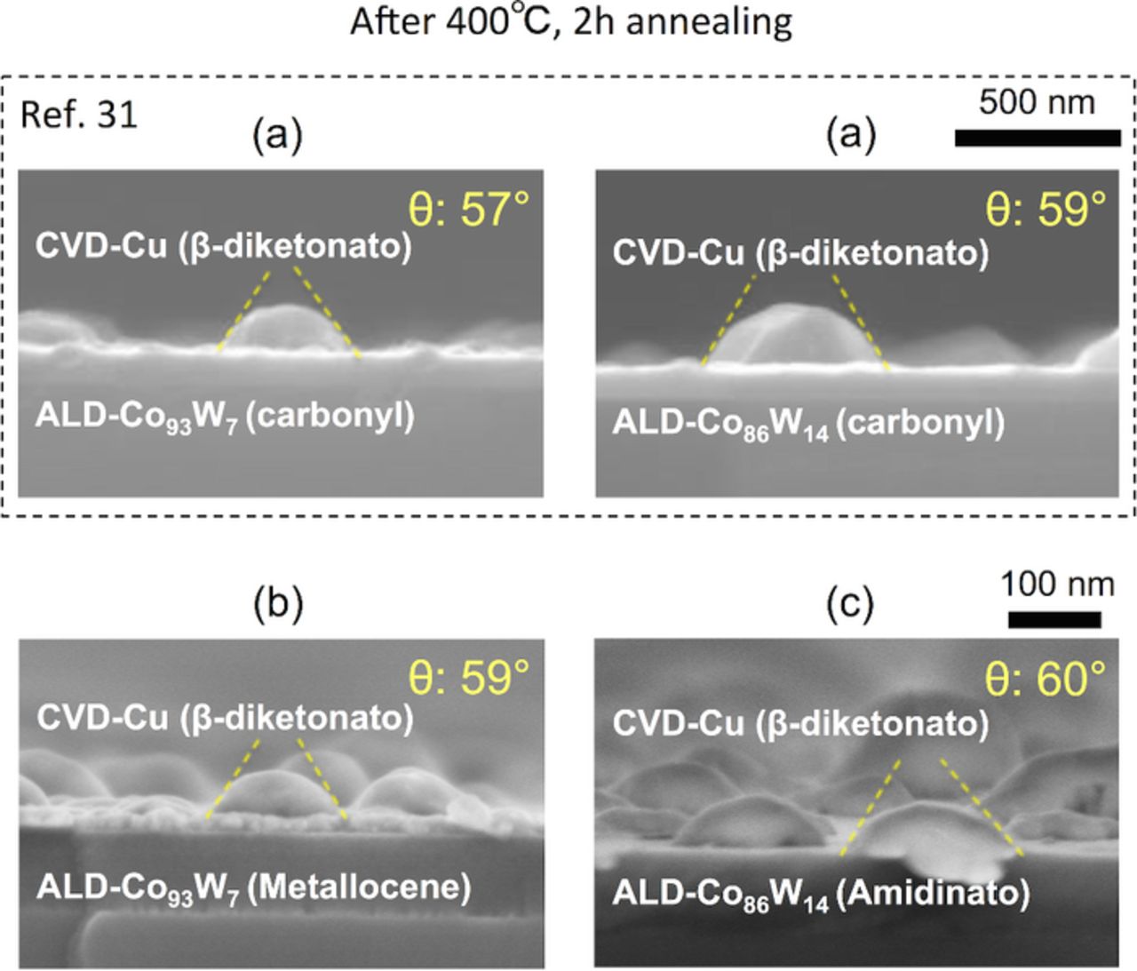
Figure 5. (Color online) FE-SEM side-views of (a) CVD-Cu (β-diketonato)/ALD-Co(W) (carbonyl) [W: 7 or 14 at%],31 (b) CVD-Cu (β-diketonato)/ALD-Co(W) (metallocene) [W: 7 at%], and (c) CVD-Cu (β-diketonato) /ALD-Co(W) (amidinato) [W: 14 at%]. The samples were annealed at 400°C for 2 h, and the corresponding average Cu wetting angles are shown.
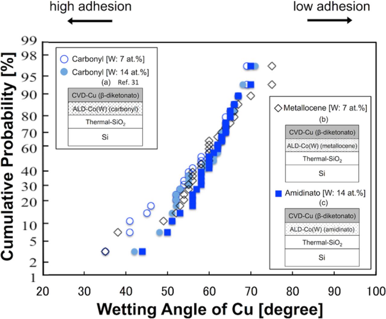
Figure 6. (Color online) Cumulative probability distribution of the Cu wetting angle on the ALD-Co(W) underlayers as a function of the Co and W precursors (carbonyl,31 metallocene, and amidinato). CVD-Cu was grown using the β-diketonato precursor in all samples.
To investigate the impact of the surface oxidation of the Co(W) on the adhesion of Cu, we investigated the adhesion strength of Cu/Co and Cu/CoOx stacks grown using sputtering. For the ease of configuring the sputtering machine, Co was fabricated in place of Co(W); however, this was considered substitutable because Co(W) is composed mainly of Co. Sputtering was employed because of the high purity of the films. Note that an investigation of Cu/W and Cu/WOx stacks was also carried out; however, we do not discuss the results of this investigation here because of poor experimental reliability caused by inter-diffusion of Cu and W. Figure 7 shows side-views of Cu grains following annealing at 180°C for 2 h. The adhesion strength was compared based on the agglomeration tolerance, rather than the wetting angle, as discussed in the experimental section. Following annealing, the Cu film formed on Co was smooth and continuous, retaining the original shape, whereas the Cu film formed on CoOx appeared hazy, and was discontinuous due to agglomeration of the Cu film. Accordingly, the surface oxidation of Co evidently degraded the wettability of Cu; i.e., the adhesion strength between Cu and underlayer was low. We therefore conclude that the adhesion strength of the Cu/Co(W) interface may also be degraded by surface oxidation of the Co(W) layer, whereby surface oxidation of underlayer concealed the inherent nature of the underlying metallic material.
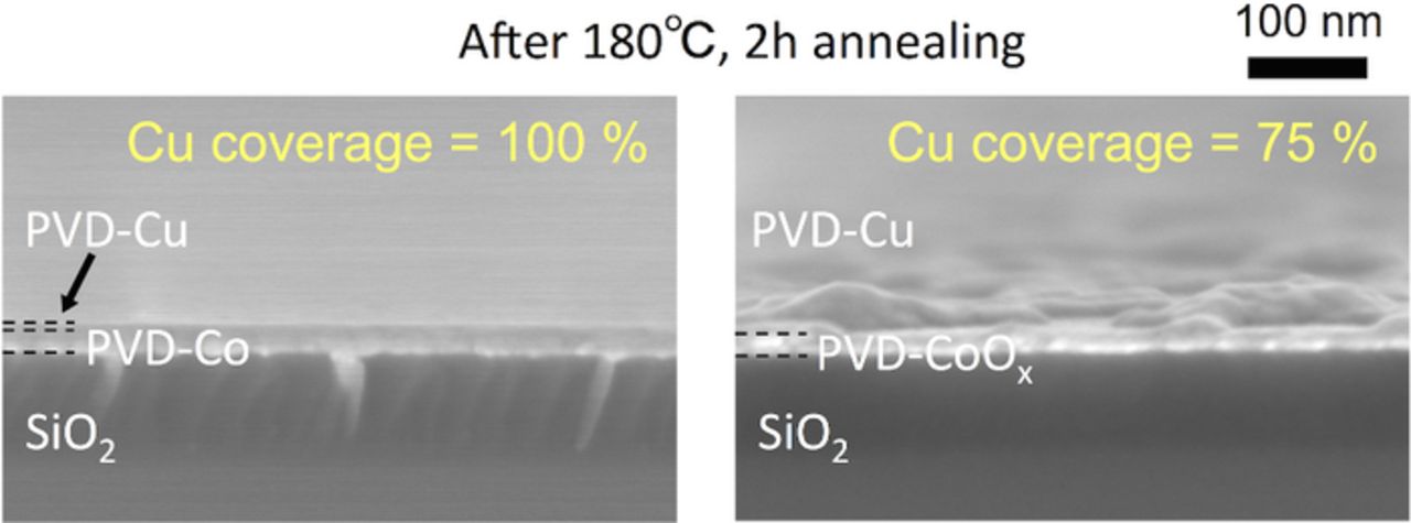
Figure 7. (Color online) FE-SEM side-views of PVD-Cu/PVD-Co and PVD-Cu/PVD-CoOx samples. The samples were annealed at 180°C for 2 h, and the corresponding Cu surface coverage is shown, as determined using XPS.
Based on these discussions, we may speculate that the elimination of O from the Co(W) underlayer by using metallocene or amidinato precursors had little impact on the Cu adhesion strength, whereas subsequent Cu-CVD should be carried out using conventional β-diketonato precursors, which includes an oxidizing agent. This is expected because secondary ion mass spectrometry (SIMS) analysis has been reported to reveal the presence of an oxide layer at the interface between the underlayer and CVD-Cu film grown using a β-diketonato precursor.54
Effects of the Cu-CVD precursor on the adhesion strength
Based on the data discussed in the previous section, it appears that surface oxidization of Co(W) during the deposition of Cu dominates the adhesion strength. In this section, we investigate the effects of the choice of Cu precursor on contamination of the underlying material during the deposition of Cu. Cu was deposited using β-diketonato (which leads to the incorporation of O) and amidinato (O-free) precursors on ALD-Co(W), which was grown using amidinato precursors. These correspond to (c) CVD-Cu (β-diketonato)/ ALD-Co(W) (amidinato) and (d) CVD-Cu (amidinato)/ALD-Co(W) (amidinato) (see Fig. 2). Note that amidinato Co(W) precursors were used. The metallocene precursor used in the previous section was so stable that it necessitates the use of an NH2 radical as a reductant, which was formed by cracking NH3 using a hot-wire system in the ALD chamber,49 whereas the amidinato precursor was deposited using pyrolysis, and thereby a conventional ALD reactor could be used without modification. The W content was fixed at 14 at% in both cases. This is because we have previously shown that the barrier properties and electrical conductivity of Co(W) exhibited trade-off relation as a function of W content, and 14 at% was found to have equivalent diffusion barrier properties to TaN, while exhibiting greater electrical conductivity than TaN.26,27,30
Table III shows a comparison of the various growth precursors in the composition of the Cu film. The incorporation of impurities, including O and F, evidently varied significantly between the Cu films grown using β-diketonato and amidinato precursors, both at the surface as well as in the film. The incorporation of O and F into the Cu film was completely eliminated using amidinato precursor, although trace amounts of C and N impurities were found. During the initial stages of the Cu growth using the β-diketonato precursor, O and CF3 are released from the ligands of the Cu precursor, and then adsorbed onto the surface of the underlayer because this surface is not fully covered by the Cu film. SIMS analysis has shown that O and F were present at the interface between the CVD-Cu (β-diketonato) and PVD-Ta layers.54 In addition, XPS analysis has been used to show that F at the interface of CVD-Cu (β-diketonato)/PVD-Ta originates from fluorinated functional groups released from ligands of this precursor.55 To investigate the presence of such impurities with the ALD-Co(W) underlayer, we carried out XPS analysis of the Cu/Co(W) interface without using conventional ion etching, rather by investigating agglomeration of the Cu films using the same procedure as the wetting angle measurements. Oxygen was clearly detected, and slightly larger Co oxides peaks were detected with the β-diketonato Cu-CVD precursor than with the amidinato precursor. However, it was not possible to identify whether the peaks corresponding to W oxides (i.e., O incorporation) occurred during Cu-CVD or during the vacuum break following the post-growth annealing, due to high reactivity of W with O. In addition, several atomic percent of F was also detected at the interface between the CVD-Cu (β-diketonato) and ALD-Co(W) (amidinato) layers, where evidence of chemical bonding of F with both Co and W was clearly shown (see Fig. 10).56–58 In summary, the existence of O and F at the Cu/Co(W) interface was apparent when β-diketonato was used as the Cu-CVD precursor. Therefore, the use of the amidinato Cu-CVD precursor is expected to prevent contamination at the surface of the Co(W) layer during CVD growth of Cu. The effects of N at the interface on the wetting angle appear to be ambiguous. This could be investigated further using similar structures formed via sputtering, which represents an area for future work.
Table III. The elemental compositions of the CVD-Cu films grown using β-diketonato and amidinato precursors, as measured using XPS.
| [at%] | ||||||
|---|---|---|---|---|---|---|
| Cu | C | N | O | F | ||
| CVD-Cu | surface | 42.9 | 28.7 | 0.0 | 24.7 | 3.7 |
| β-diketonato | inside | 96.0 | 0.7 | 0.0 | 1.0 | 2.2 |
| CVD-Cu | surface | 51.4 | 29.4 | 2.7 | 16.4 | 0.0 |
| Amidinato | inside | 98.7 | 0.4 | 0.9 | 0.0 | 0.0 |
surface: after air exposure.inside: after 3-nm-deep etch by Ar ion in XPS chamber.
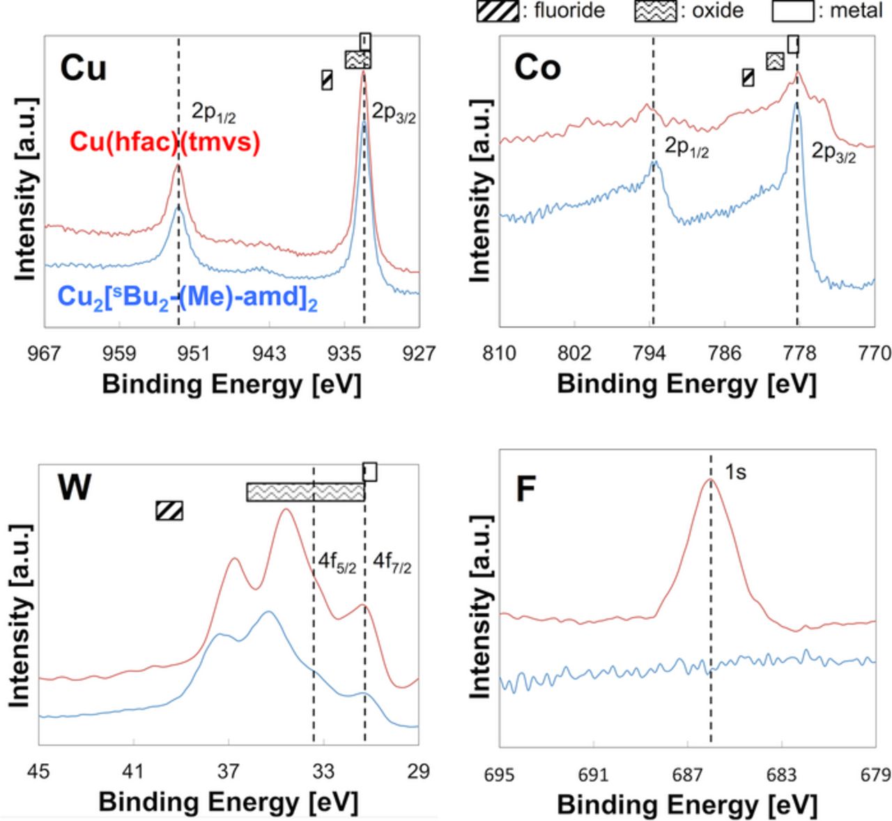
Figure 10. (Color online) XPS spectra of the Cu 2p, Co 2p, W 4f, and F 1s regions obtained for the CVD-Cu (β-diketonato)/ALD-Co(W) (amidinato) [W: 14 at%] (shown in red), and CVD-Cu (amidinato)/ALD-Co(W) (amidinato) [W: 14 at%] interfaces (shown in blue). These data were obtained by agglomerating the overlying Cu films via post-process annealing. The crossbars at the tops of the diagrams indicate the peak energies (Cu 2p3/2, Co 2p3/2, and W 4f7/2), which depend on the chemical state.56–58 Note that the W 4f peak has two components (4 f5/2 and 4 f7/2), which are separated by 2.18 eV.
Figure 8 shows representative side-views of the agglomerated Cu grains grown on the ALD-Co(W) underlayers. The wetting angles of the Cu grains extracted from the SEM images are shown in Fig. 9. The wetting angle of the Cu grains varying significantly depending on the choice of Cu precursor (60° for β-diketonato and 48° for amidinato). The effects of the choice of Cu precursor on the adhesion strength were as follows: the O- and F-free Cu amidinato precursor resulted in the higher Cu adhesion strength with the underlying ALD-Co(W) by preventing contamination at the interface of Cu/Co(W) during Cu-CVD. Note that, with PVD-Ru, no significant differences were observed in terms of the Cu adhesion strength, regardless of the Cu growth method; the average wetting angles did not vary significantly among PVD-Cu/PVD-Ru (42°), CVD-Cu (β-diketonato)/PVD-Ru (41°), and CVD-Cu (amidinato)/PVD-Ru (43°) (see Table I). As has been discussed previously, the noble Ru underlayer is expected to prevent adsorption of impurities (i.e., O and F)59,60 and to allow the formation of a clean interface with Cu, in contrast to the use of a base metal (Co(W) and Ta) as the underlayer.
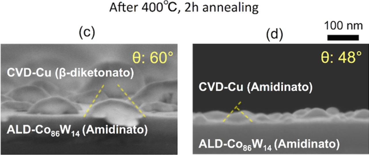
Figure 8. (Color online) FE-SEM side-views of (c) CVD-Cu (β-diketonato)/ALD-Co(W) (amidinato) [W: 14 at%] and (d) CVD-Cu (amidinato)/ALD-Co(W) (amidinato) [W: 14 at%]. The samples were annealed at 400°C for 2 h, and the corresponding average Cu wetting angles are shown.
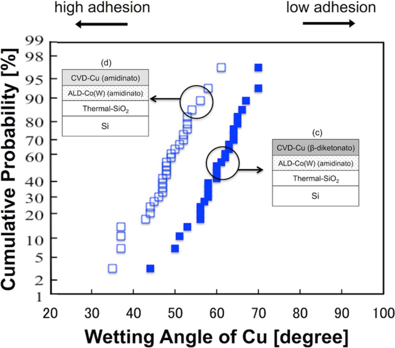
Figure 9. (Color online) Cumulative probability distribution of the Cu wetting angle on the ALD-Co(W) [W: 14 at%] underlayers for the different Cu precursors (β-diketonato and amidinato). The ALD-Co(W) layers were grown using amidinato precursors in both samples.
Effects of W content in the Co(W) layer on the adhesion strength
The W content was varied through 7, 14, 23, and 31 at%, resulting in the samples shown in Fig. 2d, i.e., CVD-Cu (amidinato)/ALD-Co(W) (amitinado). Representative side-views of the Cu grains are shown in Fig. 11. Figure 12 shows that a higher W content led to larger wetting angle, resulting in poorer adhesion strength. In the case of CVD-Cu (β-diketonato)/ALD-Co(W) (carbonyl), the wetting angle did not depend on the W content (see Fig. 6), which is attributed to the dominant effects of F and O contamination at the Co(W) surface. In contrast, the use of the amidinato Cu precursor resulted in significantly less contamination at the interface, and thereby the wetting angle was primarily determined by intrinsic properties of the Cu and Co(W) layers. A smaller W content led to improved adhesion strength because Cu has more structural affinity with Co than with W.
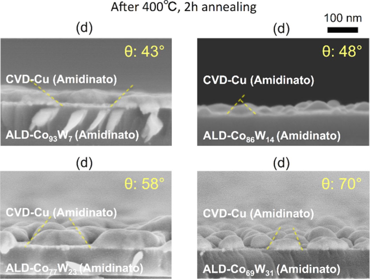
Figure 11. (Color online) Side-views of (d) CVD-Cu (amidinato)/ALD-Co(W) (amidinato). The W content was varied through 7, 14, 23 and 31 at%. The samples were annealed at 400°C for 2 h, and the corresponding average Cu wetting angles are shown.
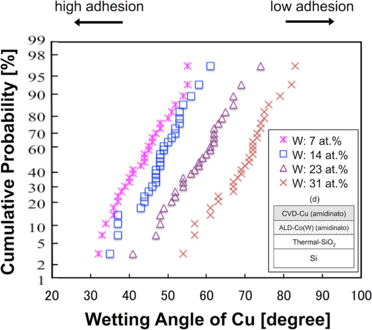
Figure 12. (Color online) Cumulative probability distribution of the Cu wetting angle on Co(W) underlayers for W contents of 7, 14, 23 and 31 at%. The ALD-Co(W) and CVD-Cu layers were grown using amidinato precursors for all samples.
Benchmarking of Co(W) with contenders for ULSI Cu interconnects
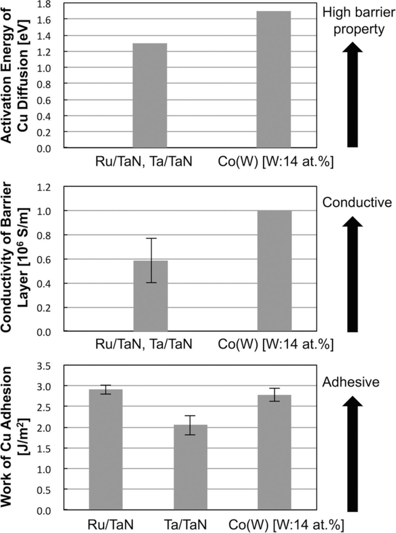
The optimal W content in the Co(W) layer for applications in ULSI Cu interconnects was investigated on the basis of the following three characteristics: the Cu diffusion barrier properties, the electrical conductivity, and the adhesion strength. We reported previously the dependency of Cu diffusion barrier properties and the electrical conductivity of Co(W) on the W content using ALD-Co(W) film grown using amidinato precursors. The findings were as follows. First, a larger W content led to improved diffusion barrier properties, and a W content greater than 14 at% led to superior diffusion performance compared with TaN27,30; second, a smaller W content led to a higher electrical conductivity, and W content of less than 14 at% provided superior electrical conductivity to that of TaN.26,30 For this reason, the adhesion strength of CVD-Cu on ALD-Co(W) [W: 14 at%], where both layers were grown using amidinato precursors, was compared with the current de facto standard materials (PVD-Cu on PVD-Ta), as well as a major contender for next generation ULSI Cu interconnects (PVD-Cu on PVD-Ru). These samples correspond to the following structures: (d) CVD-Cu(amidinato)/ALD-Co(W)(amitinado) [W: 14 at%], (e) PVD-Cu/PVD-Ta/TaN,31 and (f) PVD-Cu/PVD-Ru, respectively (see Fig. 2). Representative side-views of agglomerated Cu grains on Co(W), Ta,31 and Ru are shown in Fig. 13. Here, the obtained average wetting angle of 42° for PVD-Cu/PVD-Ru was in good agreement with the 43° reported by Kim et al.9,13 using the same structure but with different annealing conditions to cause Cu agglomeration (650°C for 20 min). The wetting angles of the Cu grains are shown in Fig. 14. The wetting angle of the Cu/Co(W) [W: 14 at%] was 48° on average, which is larger than that of Cu/Ru (42° on average) but smaller than that of Cu/Ta (77° on average).31 Based on these data, the work of Cu adhesion, Wad, was estimated using the Young–Dupré equation (Equation 4), and the results are summarized in Table IV. A surface energy of γCu = 1.67 J/m2 was used for all the cases.61 The work of adhesion for the Cu/Co(W) [W: 14 at%] interface was calculated to be 2.79 J/m2, which is similar to that reported for Cu/Ru (2.91 J/m2), and significantly larger than that for Cu/Ta (2.05 J/m2).
Table IV. The work of adhesion of Cu for PVD-Cu/PVD-Ta,31 PVD-Cu/PVD-Ru, and CVD-Cu/ALD-Co(W) stacks, as determined from the average wetting angle of agglomerated Cu grains using the Young–Dupré equation.
| Ta | Ru | Co(W) [W: 14 at%] | |
|---|---|---|---|
| Cu Wetting angle (θ) [degree] | 77 ± 1731 | 42 ± 12 | 48 ± 13 |
| Work of Cu adhesion (Wad) [J/m2] | 2.05 ± 0.46 | 2.91 ± 0.21 | 2.79 ± 0.31 |
2Surface energy of Cu (γCu): 1.67 [J/m]61.Wad = γCu(1 + cos θ).
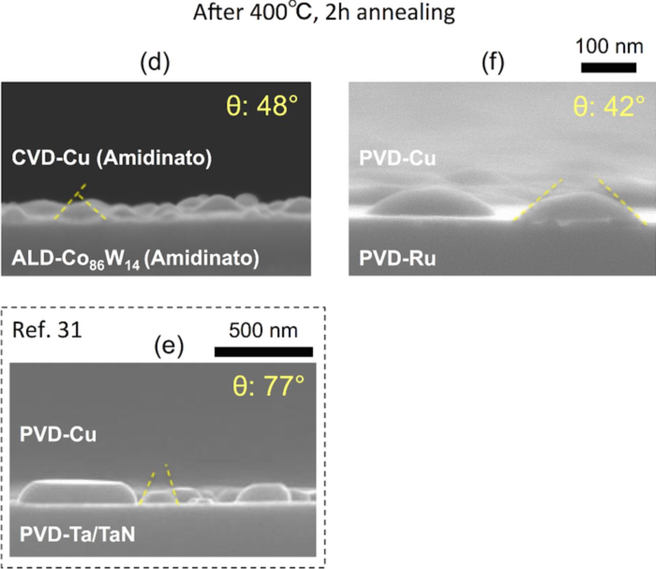
Figure 13. (Color online) Side-views of (d) CVD-Cu (amidinato)/ALD-Co(W) (amidinato) [W: 14 at%], (e) PVD-Cu/PVD-Ta,31 and (f) PVD-Cu/PVD-Ru. The samples were annealed at 400°C for 2 h, and the corresponding average Cu wetting angles are shown.
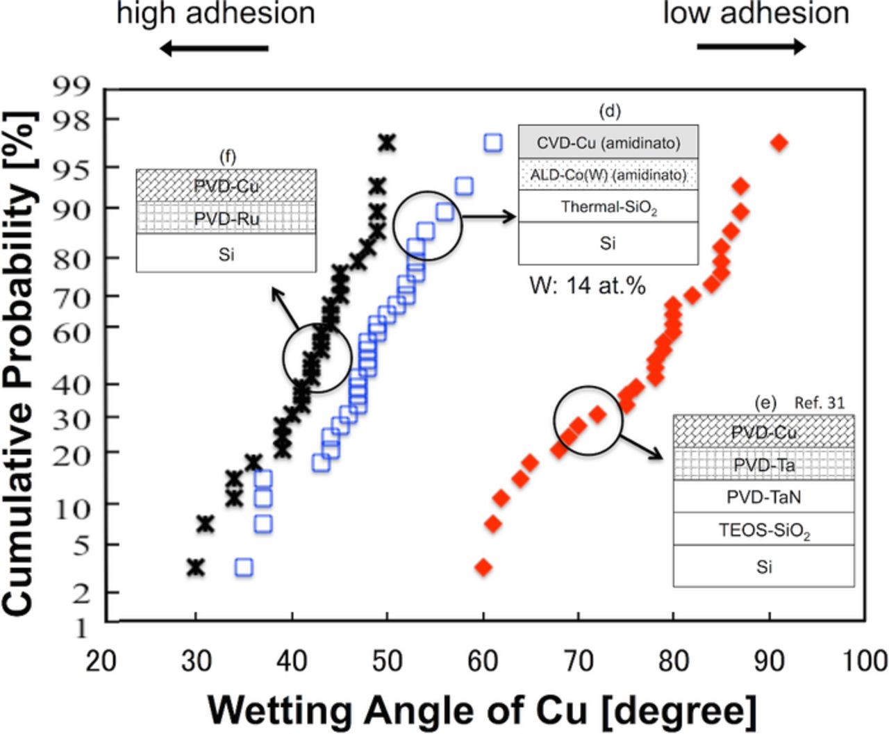
Figure 14. (Color online) Cumulative probability distribution of the Cu wetting angle on ALD-Co(W) [W: 14 at%], PVD-Ru, and PVD-Ta31 underlayers. The CVD-Cu layer was grown on the ALD-Co(W) layer using amidinato precursors for both the CVD-Cu and ALD-Co(W), whereas PVD-Cu layers were grown on the PVD-Ru and PVD-Ta layers.
The physical characteristics as a liner/diffusion barrier in ULSI Cu interconnects were compared among PVD-Ta/TaN double layers, PVD-Ru/TaN double layers, and ALD-Co(W) single layer [14 at%]. The activation energies for Cu diffusion in the barrier were compared, which is a commonly used index of the diffusion barrier properties of Cu interconnects. The electrical conductivity of the underlayers was compared (i.e., that of solely TaN or Co(W)). The use of a (single) Co(W) layer is potentially advantageous in increasing the overall line conductance. Single-layer Co(W) can be less thick than the layers formed using existing approaches, allowing more volume for Cu, hence increasing the conductance of the line compared with double-layer Ru/TaN and Ta/TaN systems. This advantage is critical for the 1x nm-nodes, where the width of the Cu line is less than 15 nm, and so the conductance of the Cu line falls considerably as the thickness of the barrier/adhesion layer increases.1,62,63
Figure 15 shows the activation energy for Cu diffusion in the barrier layer,27,30 the conductivity of the barrier layer,26,30 and work of Cu adhesion obtained in this study. As a result, a Co(W) single layer liner/barrier is favorable compared with a conventional Ta/TaN stack in terms of all three metrics, and was superior to a Ru/TaN stack in terms of the diffusion barrier properties and the electrical conductance, while similar in terms of the adhesion strength. We may therefore conclude that ALD-Co(W) is a promising candidate materials system for applications as a liner-barrier material for next-generation ULSI Cu interconnects.
Conclusions
We have investigated the properties of ALD-Co(W) as a single layer that can function as both a barrier to Cu diffusion and as a liner to promote the adhesion of Cu. The use of oxygen-containing Co and W precursors, such as carbonyls, has been reported to lead to lower electrical conductivity and poorer barrier performance due to incorporation of O into the film; for this reason, the O-free metallocene and amidinato precursors were used in this work. We successfully achieved O-free Co(W) deposition using a β-diketonato Cu precursor, with a large electrical conductivity and favorable diffusion barrier properties; nevertheless, good adhesion strength between CVD-Cu and ALD-Co(W) was not obtained because of the presence of O and F impurities due to the use of a β-diketonato Cu precursor, which was found to contaminate the surface of the Co(W) layer during deposition. The use of an amidinato Cu CVD growth precursor, which includes neither O nor F, enabled an adhesion strength that depended on the inherent properties of the Cu and Co(W) materials. For this reason, the effects of the W content in the Co(W) layer on the adhesion strength with Cu could be investigated. A smaller W content was found to lead to a higher adhesion strength between the Co(W) underlayer and the Cu. The optimal composition of the ALD-Co(W) layer was found to be 14 at% W, which provides a trade-off between the diffusion barrier properties, the electrical conductivity, and the adhesion strength with the Cu. The optimized ALD-Co(W) was benchmarked based on these three characteristics against PVD-Ta/TaN (the current de facto materials system) and PVD-Ru/TaN (a promising candidate next-generation materials system). We find that the single-layer ALD-Co(W) was superior to PVD-Ta/TaN in terms of all three of these characteristics, and was superior to PVD-Ru/TaN in terms of the diffusion barrier properties and total line conductance, while being comparable in terms of adhesion the strength with Cu. For these reasons, ALD-Co(W) is a promising material for the fabrication of reliable and high-performance next-generation ULSI Cu interconnects.
Acknowledgment
The authors would thank Dr. D. Hong of The Dow Chemical Company for providing us with the Cu2[sBu2-(Me)-amd]2 growth precursor, and Dr. T. Nogami of IBM for providing us with PVD-Ru/TaN/SiO2/Si wafers for Cu-CVD.