

Abstract
In this work we realized a device of silver nanostructures designed so that they have a great ability to sustain the surface-enhanced Raman scattering effect. The nanostructures were silver self-similar chains of three nanospheres, having constant ratios between their diameters and between their reciprocal distances. They were realized by electron beam lithography, to write the pattern, and by silver electroless deposition technique, to fill it with the metal. The obtained device showed the capability to increase the Raman signal coming from the gap between the two smallest nanospheres (whose size is around 10 nm) and so it allows the detection of biomolecules fallen into this hot spot. In particular, oligonucleotides with 6 DNA bases, deposited on these devices with a drop coating method, gave a Raman spectrum characterized by a clear fingerprint coming from the hot spot and, with the help of a fitting method, also oligonucleotides of 9 bases, which are less than 3 nm long, were resolved. In conclusion the silver nanolens results in a SERS device able to measure all the molecules, or part of them, held into the hot spot of the nanolenses, and thus it could be a future instrument with which to analyze DNA portions.
Export citation and abstract BibTeX RIS

Content from this work may be used under the terms of the Creative Commons Attribution 3.0 licence. Any further distribution of this work must maintain attribution to the author(s) and the title of the work, journal citation and DOI.
1. Introduction
Metallic nanoparticles and clusters of metallic nanoparticles are known and widely used for their improved optical properties. Metal nanostructures or particles can generate and maintain localized surface plasmons (LPS) [1–7], which are collective oscillations of electrons on a metal surface stimulated by an external coherent electromagnetic radiation (i.e. a laser).
When the diameter of those particles is significantly lower than the wavelength of the excitation laser, d ≪ λ, electrons on the metal surface and the excitation wave have the same phase. This in turn induces polarization charges and the formation of a dipolar field on the surface with an increase of the electromagnetic field in close proximity of the particles. The described EM amplification may be as large as several orders of magnitude which is the reason why nanostructured substrates are being increasingly used in combination with Raman spectroscopy, where the Raman signal is proportional to the EM field on the substrate. The described surface-enhanced Raman scattering (SERS) effect boosts the sensitivity of spectroscopy and in this nanotechnology evolution Raman can detect low to ultra-low concentrated solutions, with a resolution that, in the most favorable conditions, has been demonstrated to be as low as that of a single molecule [8–11].
The SERS effect can be achieved using noble metal nanoparticles of different sizes and shapes (nanospheres, nanorod, nanostars, etc) either in suspension or as aggregates deposited on a substrate [12]. The rational design of nanoparticles or nanostructures represents an important advance in SERS, in that specific geometries may allow the confinement of the EM radiation in extremely small areas, few nanometers per side, which are the active sites (hot spots) of the device: incidentally many molecules have a similar length scale of the described hot spots. Individual molecules that are deposited (entirely or in some of their parts) on these can be detected using Raman [13–15].
Recent advances in nanofabrication techniques, including lithographic techniques, focused ion beam (FIB), or self-assembly [14, 16–24], permit a tight control of the shape and size of the metal nanostructures and thus the fabrication of SERS substrates for single molecule detection.
Here we describe the realization of silver nanostructures by means of electron lithography and a simple and cost effective technique known as electroless metal deposition.
Electroless deposition is based on the autocatalytic reduction of metal salts, by means of reducing agents, on the interface with substrate. An electrons exchange occurs between metallic ions and the reducing agent, which may be in solution or may be the substrate itself. Several metals were deposited with this technique, as silver, gold, copper, nickel or their alloy, obtaining thin films, sub-micrometric metallic structures or nanoparticles [25–29]. In electroless deposition, fluoridric acid solution is used without the use of other chemicals or electric current because Si itself is a reducing agent for the reaction, as described in the methods of this paper and references [30–33].
Using the described electroless techniques, we deposited Ag nanoparticles from the AgNO3 metal salt on a silicon-patterned substrate. In doing so, we fabricated a self-similar chain of silver nanospheres, which is an ensemble of three spheres in a line in which the diameter and gap of those spheres is progressively reduced and the ratio between these is constant (this is the meaning of self-similar):


where Ri is the radius of the nanosphere i, d is the distance between two consecutive nanospheres and k is constant. In the general case of a cascade of n-nanospheres, the local field enhancement gn = En/E0 = Q(Rn/R1)lnQ/lnκ, where Q is the resonance quality factor (ratio of real and imaginary part of relative dielectric function) which depends overall from the ratio of nanospheres radius and gaps. Considering that the SERS enhancement coefficient is approximately on the order of the fourth power of the local field enhancement g, the maximum signal amplification is GSERS = Q4n, where n is the number of devices in the structure [34, 35]. For the present configuration, Q ∼ 30 and n = 3, and thus the maximum, theoretical Raman signal amplification is GSERS = 1012.
Then, we demonstrate the devices for the analysis and DNA sequencing of oligonucleotide chains. Furthermore, the fitting procedure was implemented on the substrate with a matrix of m × n SSC nanostructures in order to exhibit the fraction of nucleotides present on an individual SSC structure.
2. Material and methods
Silver nanostructures were fabricated using a process in two steps (figure 1): (i) patterns of nanoholes organized as self-similar chain of spheres, were designed by electron beam lithography on a layer of electronic-resist spun onto a silicon wafer; (ii) the metal nanostructures were grown in the pattern by electroless deposition.
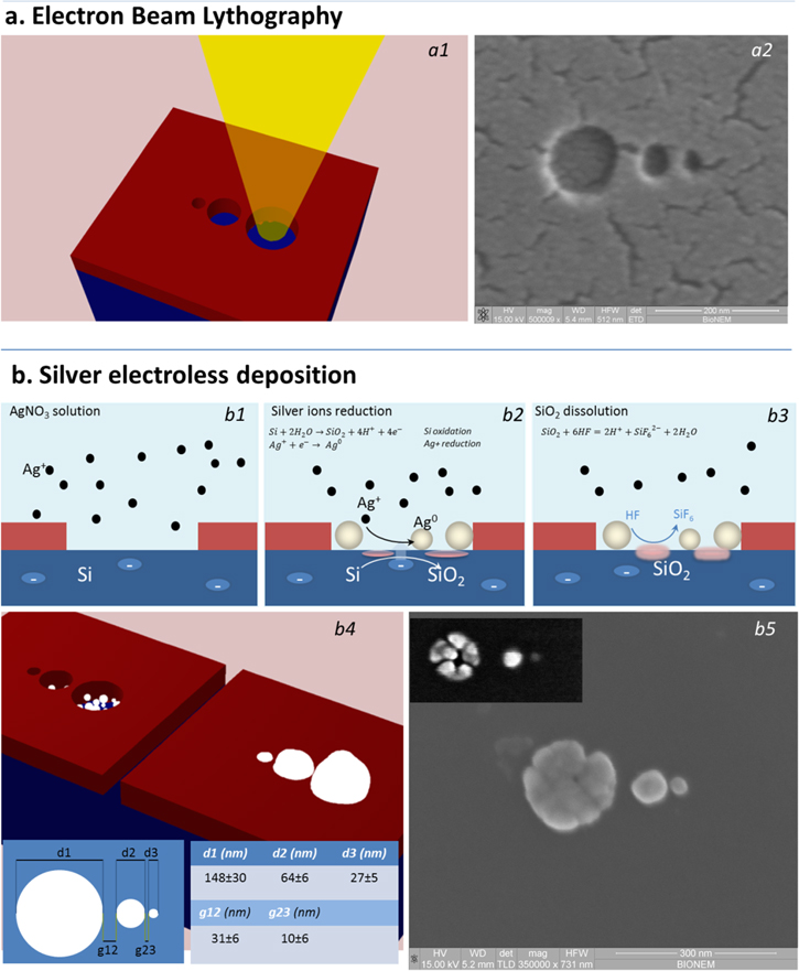
Figure 1. Nanolense fabrication: (a) electron beam lithography; (b) silver electroless deposition. In detail, for the lithographic step, the figure shows: (a1) the scheme of the lithographic process and (a2) the correspondent SEM image of the obtained pattern; meanwhile, regarding the second step of deposition is evidenced: (b1) the contact between a silicon substrate, patterned with PMMA resist, with an AgNO3 aqueous solution, (b2) the electrons exchange between the silicon and the silver ions, (b3) the dissolution of silicon oxide, produced in the previous reaction, in fluoric acid, (b4) a schematic representation of silver nanograin growth into the pattern and a table showing diameters and gaps of the three nanospheres, (b5) SEM image of the silver nanolens (in the box an intermediate step of silver growth).
Download figure:
Standard image High-resolution image2.1. Lithographic process
Standard, Si wafer (p-type, 5–10 Ω cm−1 resistivity) was used as a substrate. An electronic sensitive resist, PMMA-A2, was spin-coated for 60 s and 5000 rpm (PMMA) to obtain 50 nm thick layers. Prior the EBL exposure, the sample was pre-baked at 170 °C for 2 min to remove the solvent. The patterns of nanoholes were exposed using a Crestec CABL-9000C e-beam lithography system, operating at 30 keV acceleration voltage and a beam current of 100 pA. The samples were developed for 60 s in isopropyl alcohol at 4 °C.
2.2. Electroless silver NPs growth
De-ionized (DI) water (Milli-Q Direct 3, Millipore) was used for all experiments. Silver nitrate (AgNO3) was purchased from Sigma. Hydrofluoric acid (HF) was 50% RPE ACS-ISO, Carlo Erba Reagents. All chemicals, unless mentioned otherwise, were of analytical grade and were used as received. The Si wafer (100) was properly cleaned with acetone and ethanol to remove possible organic contaminants.
The electroless silver deposition occurs by following a redox reaction between silver nitrate (oxidizing agent) and the silicon substrate (reducing agent). The driving force of the process is the potential difference ΔE between the two half-reactions. The Nernst equation provides the relation between ΔE and the constant of equilibrium Ke of the global redox reaction:

where R = 8.3143 J mol−1 K is the universal gas constant; T is the absolute temperature of the system; F is the Faraday constant; n is the number of electrons transferred in the reaction. The parameters which influence this reaction are principally the concentration of AgNO3 in solution, the temperature and the time of the process. The lithographic pattern, in terms of absolute size and the density of nanostructures in the pattern, can also guide silver growth [36, 37]. Considering all this and the experimental results presented in [36, 37], the parameters of growth were conveniently chosen: the patterned Si substrates were immersed in a solution of HF 0.15 and AgNO3 0.05 mM for 20 s, at a solution temperature of 50 °C. The reactions were stopped by rinsing the substrates in fresh deionized water.
2.3. Finite difference time domain (FDTD) simulation
Finite difference time domain (FDTD) simulation is performed using the commercial package Lumerical Solution Inc. The design of the nanostructure was made to mimic the experimentally fabricated device. The whole structure (cascade nanostructures with 2 and 3 nanospheres) is based on silver metal, lying over a polymer layer (dielectric constant of 1.4) coated over SI substrate. The design comprises the minimum gap of 5 nm between two smaller nanospheres. The perfectly matched layer (PML) is created around the cone to avoid any simulation problem with open boundary design. A subgriding method is employed to achieve the mesh size down 2 × 2 × 2 nm3 to have spatial resolution of this order.
2.4. Sample SEM characterization
SEM images of the samples were captured using a Dual Beam (SEM-FIB)—FEI Nova 600 NanoLab system. During the acquisitions, the beam energy was set at 15 keV, and the corresponding electron current at 0.14 nA.
2.5. SERS analysis
Micro-Raman spectra (inVia Renishaw) were excited by a 514 nm laser line through a 150X objective with a laser power of 12 μW. For these analyses a drop-coating deposition method was used for depositing different oligonucleotides and λ-DNA fragments with a concentration of 10−5 mM on the SERS substrate. A more concentrated drop (0.1 M) of each nucleotide was deposited, dried and measured with Raman spectroscopy on silver sputtered substrates for comparison. The range of analysis was 1150–1800 cm−1 which comprises the most substantial peaks of the four DNA bases (adenine, guanine, cytosine, thymine). For each oligonucleotide 10 Raman mapping analyses were made in correspondence of 10 nanolenses in the matrix. From each map the most significant spectrum has been recorded and compared with those of other oligonucleotides and with those of DNA bases.
2.6. Fitting of the Raman spectra
Oligonucleotides are short DNA molecules. Here, the Raman signal of the oligonucleotides were fitted using a linear combination of the nucleobases A, C, G, T. Individual spectra of the oligonucleotides were acquired using the procedure described in the methods section. They were normalized to 1 using the maximum peak intensity contained in the acquisition range, that is flow < f < fup (flow = 1050 cm−1, fup = 1800 cm−1), and divided into n = 12 equally spaced intervals. By doing so, a finite subset of l = n × m linearly independent spectra was obtained, S = S11,..,s1m,..,sn1,..,snm; where n = 12 is defined above, m = 4 is the number of bases, and s is a generic basis for the lattice of different possible combinations of A, C, G and T. A generic combination of A, C, G and T and Raman spectrum sM thereof, can be fitted, with good accuracy, by the function

where the index i runs through the number of bases m (i = 1,.., m), while j runs through the number of intervals n (j = 1,.., n). In equation (1a, 1b), the coefficients xij are found as the best combination that minimizes the sum of the squares of deviations of Y from the experimental values sM.
From these, the functions, or weights, ξi

may be derived, that indicate the mass fraction of the component i to the total solution. And thus, the larger ξi, the more major the content of the peptide i in the mixture. Notice that the sum of the functions ξi over all the peptides m should be one. On the right-hand side of equation (2), the quantity

represents the Raman spectrum of the ith base contained in the solution, as derived from the fitting procedure. The goodness of fit metrics was verified by two parameters, namely (i) the chi square statistics, χ2, and (ii) the coefficient of determination, r2.
Where the coefficient of determination, r2, is a statistical measure of how close the data are to the fitted regression, it is the percentage of the response variable variation that is explained by a linear model, and is found as the ratio of the explained variation to the total variation or, in mathematical terms:

In which cov and σ stand for the covariance and standard deviation operators, respectively.
Similarly to r2, the Pearson's chi-squared test, χ2, is a statistical test applied to sets of categorical data to evaluate how likely it is that any observed difference between the sets arose by chance. It is suitable for unpaired data from large samples. Its value may be derived as

3. Results and discussion
3.1. Fabrication of the substrates
Metal nanostructures were obtained combining a top-down method with a bottom-up one: (i) electron beam lithography, for the pattern definition onto a PMMA-A2 spin-coated silicon wafer; (ii) electroless deposition to fill the pattern with silver nanoparticles.
The patterns are matrices composed of self-similar chains of spheres, in the following indicated as nanolenses (NLs). The dimensions and reciprocal distances (gaps) of those spheres were chosen to obtain the maximum Raman signal enhancement, as indicated in [34, 35]. Previous studies on electroless deposition into patterns in which pattern size and pattern distance were independently varied [36, 37] also indicate that, under the controlled conditions of deposition, metal nanostructures grow in a spherical shape, exceeding the dimensions of the lithographic pattern. At a small nanometer scale at which any vanishingly small deviation of few nanometers or less from the nominal parameters may change the optical behavior of the nanostructure, the rational design of the lithography was crucial to obtain the final structures in which the smallest sphere has a diameter of 20 nm and the smallest sphere to sphere gap is as small as 10 nm.
A table showing the nanospheres' dimensions and distances is reported in figure 1(b4). In the same figure, the complete scheme of the fabrication process and the SEM images of the final structures are also reported.
3.2. FDTD calculations
FDTD calculation for self-similar structure with 2 and 3 nanospheres were performed. The electric field distribution for both the structures is shown in figure 2. The figure shows that the hot spot in between the two nanospheres has the electric field around 16 V m−1 with respect to the incident one. In the case of two nanospheres the electric field is much lower. To make a clear comparison, the plots were made with the same maximum electric field.

Figure 2. 2D electrical field map of a system at 3 and 2 nanospheres. The field intensity distribution depends on the presence of the smallest nanosphere. In the configuration at three nanospheres the dimensions are: d1 = 180 nm, d2 = 60 nm, d3 = 20 nm and gaps g12 = 40 nm, g23 = 10 nm; in the configuration at two nanospheres the dimensions are: d1 = 180 nm, d2 = 60 nm and g12 = 40 nm. The wavelength chosen for simulation was 515 nm.
Download figure:
Standard image High-resolution image3.3. SERS analysis on oligonucleotides and λDNA
Raman mappings in the areas around the NLs were collected after drop-coating deposition of oligonucleotides and λ-DNA. The sketch in figure 3 reproduces what happens when a layer of a biomolecule is the deposited on the substrate and Raman analysis is performed: the Raman signal only comes from the hot spot of a nanolens, making visible the molecules or the portions of them held in that area.
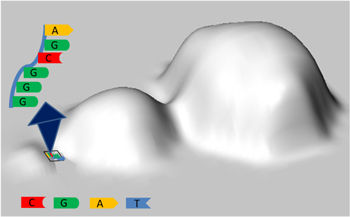
Figure 3. Schematic representation of a Raman analysis on a layer of biomolecule covering a NLs: the Raman signal only comes from the gap between the two smallest nanospheres.
Download figure:
Standard image High-resolution imageRaman analysis on oligonucleotides, as described in the following, confirm the strong localization of the EM field for the nanolense device.
Oligonucleotides with 6 and 9 bases were analyzed. In this case, the difference between different sequences is restricted to very few bases. In what follows, we report specific sequences with the corresponding spectra.
In figure 4 the gray area on the optical image, obtained with a 150X objective, evidences a typical Raman mapping which covers a region with several (more than one) nanolenses (the dark points in the image) within it, after drop-coating deposition of an oligonucleotide, which in this case is p9 (CCCGTT). The most relevant spectra from each nanolens have been selected and have been compared to each other and to the spectra of individual DNA bases.

Figure 4. Oligonucleotide p9 (CCCGTT): (a) optical image of Raman mapping on two nanolenses; (b) SERS spectra obtained in the two hot spots of the Raman mapping for oligonucleotide p9, compared with SERS spectra of the three DNA bases present in its sequence. The colored bands evidence some of the principal peaks of the three nucleotides.
Download figure:
Standard image High-resolution imageIn particular, the two spectra on the left-hand side of figure 4 were collected from two different nanolenses. These SERS spectra exhibit few common bands and the appearance and disappearance of other vibrational bands. This can be explained explicitly by the orientation of the adsorbed molecules on the surface [38, 39]. Over different nanolenses on the substrate, it seems the molecules are adsorbed in a different manner.
In particular, the black spectrum shows a major weight of the peaks of cytosine (1248, 1285 and 1528 cm−1; see the right side of figure 4) as expected considering the prevalence of this base in this oligonucleotide; nevertheless, in the red one, guanine and thymine are more influent. The hot spots in the nanolens measure about 10 nm and so they can contain at most 3–5 molecules of one oligonucleotide with 6 bases. A different spatial arrangement of such molecules into the hot spot could be the reason for the dissimilarities of the SERS spectra as in figure 4.
For sake of clarity we report in table 1 the band position, the possible vibrational assignment and the DNA bases containing the specific vibration for the oligonucleotide p9 (CCCGTT).
Table 1. Assignments of Raman shift for oligonucleotide p9 (CCCGTT).
| Band position cm−1 | Assignment | Base | Reference |
|---|---|---|---|
| 1174–1208 | Ring s, CN s, C-Me s | T, C | [40, 41] |
| 1248–1288 | Ring s | C, T | [40, 41] |
| 1408 | CN s | G, C | [40] |
| 1447–1486–1537 | CN s e CMe b | G, C, T | [40, 41] |
| 1570–1575 | CN s | G | [40] |
| 1604–1700 | C=O s | G, T | [40, 41] |
Abbreviations: r = rocking; s = stretching; b = bending.
The oligonucleotide p10 (GGGCAA) in figure 5 shows a pronounced presence of guanine and adenine in all the acquired spectra, with peaks emerging in the 1400–1585 cm−1 range, which justify the large band in that range.

Figure 5. SERS spectra collected from different nanolenses for oligonucleotide p10 (GGGCAA), compared with SERS spectra of the DNA bases present in its sequence. The colored bands evidence some of the principal peaks of the three nucleotides.
Download figure:
Standard image High-resolution imageTo assess the capability of these nanolenses to discriminate between nucleotides, we have compared two similar oligonucleotides, which are p10 (GGGCAA) and p7 (GGGCGG), where the number of bases is the same and the difference between the two is limited by the (A) basis that is replaced by (G) in p7.
In the case of p7, the spectra are similar to those of the p10 oligonucleotide, except that some peaks of guanine are evidenced because of the increased content of this nucleotide in the polymer; coherently, the bands of adenine disappear (figure 6 and table 2). Especially notice the change in the 1300–1350 cm−1 range, where in the presence of adenine (thus, p10) it is possible to distinguish two peaks: positioned at 1310 cm−1 and 1330–1340 cm−1. When adenine is substituted with guanine (thus, p7) only one peak becomes visible roughly in the 1325–1330 cm−1 band gap. The small band shifts in the different spectra for the same oligonucleotide may be ascribed to random molecular orientations within each hot spot, as mentioned above.
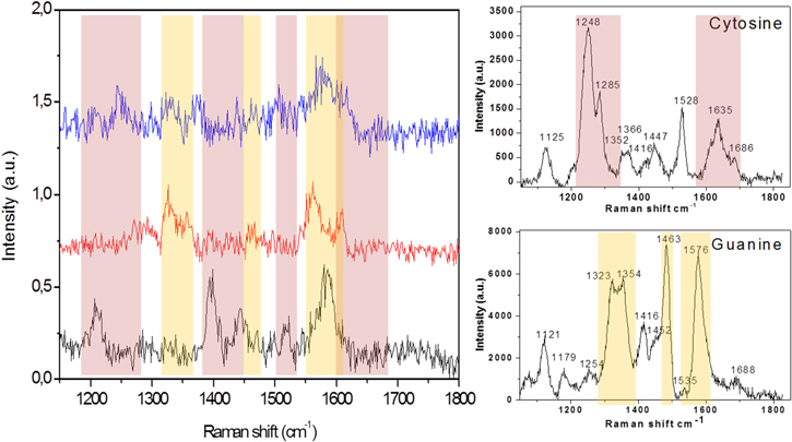
Figure 6. SERS spectra collected from different nanolenses for oligonucleotide p7 (GGGCGG), compared with SERS spectra of the DNA bases present in its sequence. The colored bands evidence some of the principal peaks of the two nucleotides.
Download figure:
Standard image High-resolution imageTable 2. Assignments of Raman shift for oligonucleotide p10 (GGGCAA) and p7 (GGGCGG).
| Band position cm−1 | Assignment | Base | References |
|---|---|---|---|
| Oligonucleotide p10 GGGCAA | |||
| 1200 | Ring s, CN s | C | [40] |
| 1270–1285 | Ring s, CN s | C | [40] |
| 1310–1330 | CN s | A, G | [40, 42] |
| 1416–1445–1488 | CN s e CH b | G, C, A | [40, 42] |
| 1520–1525 | CN s | C | [40] |
| 1534–1590 | NH2 sciss | A, G | [40, 42] |
| 1604 | C=O s | G | [40] |
| 1680 | C=O s | C, G | [40] |
| Oligonucleotide p7 GGGCGG | |||
| 1200–1205 | Ring s, CN s | C | [40] |
| 1270–1285 | Ring s, CN s | C | [40] |
| 1325–1330 | CN s | G | [40] |
| 1445–1507 | CN s e CH b | G, C | [40] |
| 1557–1590 | NH2 sciss | G | [40] |
| 1604–1616 | C=O s | G | [40] |
Abbreviations used: r = rocking; s = stretching; b = bending.
The principal peaks, with their assignments for oligonucleotides p10 and p7, are reported in table 2.
Then, we analyzed a long sequence nucleotide (p2), its sequence being CCC GCC GCT. Even in this case, the dimension of the nucleotide is less than 3 nm and thus between 2 and 3 molecules may fall into the hot spot of the nanolenses. For this, the spectra of different nanolenses and the peak assignments are reported in figure 7 and table 3.
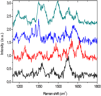
Figure 7. SERS spectra of oligonucleotides p2 (CCC GCC GCT) collected from different nanolenses.
Download figure:
Standard image High-resolution imageTable 3. Assignments of Raman shift for oligonucleotide p2 (CCC GCC GCT).
| Band position cm−1 | Assignment | Base | References |
|---|---|---|---|
| 1190–1198 | CN s NH b | C | [40] |
| 1269–1272 | Ring s, CN s | C | [40] |
| 1341 | CN s | G | [40] |
| 1386–1444 | CN s, C-Me b | G, C, T | [40, 41] |
| 1507, 1518 | CN s | C | [40] |
| 1580–1590 | CN s | G, T, C | [40, 41] |
| 1604–1616 | C=O | G, C | [40] |
Abbreviations used: r = rocking; s = stretching; b = bending.
A fitting procedure (see methods) was performed on the described oligonucleotide. From this (figure 8) the relative content of the A, C, G, T bases was derived; notice that their total is one.
- A = 0.044
- C = 0.565
- G = 0.2256
- T = 0.161
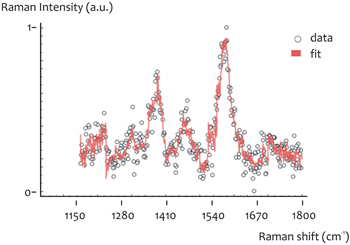
Figure 8. Fitting of a SERS spectrum of oligonucleotide p2 (CCC GCC GCT).
Download figure:
Standard image High-resolution imageThese values are comparable to the theoretical, which are:
- A = 0
- C = 0.6667
- G = 0.2223
- T = 0.1111
The fitting procedure works perfectly also for the oligonucleotides with 6 bases, and data are reported in a separate section (SI1, available from stacks.iop.org/JOPT/17/114021/mmedia). The described mathematical procedure demonstrates that, in considering an array of nanolenses or other similar sensing devices, data analysis and mathematical modeling cannot be neglected. In a similar device, determining the oligo-bases' content in a sample (that is, the response of the system) results from a sequence of tightly interweaving processes, i.e. (i) fabrication, (ii) Raman measurement and (iii) data analysis. The nanolenses' object is less a collection of these components in isolation and more a complex system in which interaction among its components yields cooperative phenomena with improved abilities in contrast to isolated components of that system.
Assuming that the DNA molecule forms a line joining the two centers of the smaller spheres, the maximum length that a sequence of nucleotides should have to match the gap would be 10 nm, which corresponds to about 31 bases. Differently, assuming that the molecules of oligonucleotides are disposed horizontally, the length of the DNA strand would be roughly 5 nm (that is comparable to the radius of the smallest sphere) that is equivalent to 15 bases.
This would justify the results of the analysis on oligos with 16 bases and 33 or more bases (figure 9). The oligos with 16 bases show very similar spectra, although with some different peaks, probably due to the positioning of the molecule in the interaction with silver grains; on the other hand oligos with a number of bases greater than 30 give very different spectra which depend on the specific portion of molecules that have fallen in the hot spot.

Figure 9. Spectra measured on various nanolenses of λDNA portions with two different lengths: on the left side a filament of 12 bases and on the right side a filament of 33 bases.
Download figure:
Standard image High-resolution image
This is not the first time that DNA and oligonucleotides were analyzed utilizing the SERS effect, which appears very attractive for the efficiency of the technique and because it also allows a label-free analysis. Usually these studios exploit the SERS effect in microfluidic applications for the detection of oligonucleotides at very low concentrations. Combining SERS with a microfluidic device, SERS spectra of oligonucleotides (at 1–2 nm) were obtained as fingerprints to detect label-free RNA [43]. Label-free oligonucleotides, induced by spermine, at 12–14 bases and concentration 10−7 M (double helix) were also analyzed, obtaining SERS spectra very close to those of the normal Raman spectra of free DNA, allowing the detailed assignment of the vibrational modes [44].
Recently SERS systems for the specific individuation of a biomarker has also been developed. Karaballi et al have implemented an electrochemical surface-enhanced Raman spectroscopy aptasensor based on a silver nanoparticle functionalized for direct and specific detection of DNA hybridization as an instrument of diagnosis in tuberculosis [45].
Our method departs from the other described methods in that it is based on well-defined silver nanostructures, designed for yielding maximum SERS effects, and it is used in combination with a data analysis technique. The integration of the two allows the label-free detection of DNA or portions of DNA and, perhaps more importantly, it can provide information on single mutation or very small fragments of nucleic acids, which can be manifested as small peaks in the Raman spectrum otherwise invisible to Raman or conventional SERS systems.
4. Conclusions
In this work electron beam lithography and electroless deposition were combined to obtain SERS devices capable of increasing the Raman signal and to detect oligonucleotides and DNA primers with a resolution depending on the molecules' length. The SERS devices are composed of arrays of silver nanostructures constituted of self-similar chains of three nanospheres, where the gap between the two smallest nanospheres is as small as 10 nm. This area represents the hot spot in which the SERS effect reaches its apex, as indicated by the work of Stockman, and consequently the molecules, or the portion of them which fall in it, become Raman 'visible': clear spectra could be obtained representing their chemical fingerprint and spatial organization.
In the specific case of DNA and oligonucleotides, it is known that a single nucleotide has a length of 0.33 nm, thus a sequence of nucleotides disposed in line with the axis of the self-similar chain would be completely contained into the hot spot of the nanolens if its length is around 30 nucleotides.
Supposing that the oligonucleotides are aligned perpendicular to the above-mentioned axis and considering an active area in this direction to be as large as the radius of the smallest sphere (5 nm), the number of nucleotides are about 15. Experimentally we obtained, in fact, that for oligonucleotides of 6 or 9 bases, Raman spectra on different nanolenses differed overall for the intensity of the peaks or for small band shifts due, principally, to the spatial organization of the molecule. Each spectrum is therefore representative of the analyzed oligonucleotide and a fitting process, which utilizes the DNA bases' spectra, is able to calculate its composition in the DNA bases. We point out that a future application of this method can be of great interest in the study of DNA–protein interaction, for example in DNA repair, where the spatial resolution demonstrated here matches the needed resolution for these structural studies. In conclusion, we have realized a powerful SERS device that works as a nanolens revealing molecules, or parts of them, when there are very few or are very small in size, as opposed to the contentional analysis methods which need a certain quantity of molecules. This device, coupled with an opportune method for realizing tensions and a strand of a DNA filament, could become a relevant technique for DNA sequencing.
5. Acknowledgments
The authors gratefully acknowledge financial support from Cariplo Foundation under the project 'New Frontiers in Plasmonic Nanosensing' (grant no. 2011-0338), from the EU Commission, the European Social Fund and the Calabria Region (POR Calabria FSE 2007–2013) and from the Italian Minister of Health under the project 'Cancer biomarker detection using micro-structured/super-hydrophobic surfaces and advanced spectroscopy techniques' (project no. GR-2010-2320665) and 'High Throughput analysis of cancer cells for therapy evaluation by microfluidic platforms integrating plasmonic nanodevices' (project no. GR-2010-2311677). This work was also partially supported by the European project EUROMBR (grant no. 608104).