

Abstract
Surface-enhanced Raman spectroscopy (SERS) is a powerful optical sensing technique used in various applications, including medicine, microbiology, and environmental analysis. Planar SERS substrates are of particular interest due to their ease of integration in lab-on-chips and better reproducibility compared to colloidal SERS. The performance of these SERS substrates is quantified using metrics such as enhancement factor, sensitivity, and reproducibility. However, there is yet to be a consensus on how to practically compare and interpret such metrics in publications and experiments. These performance metrics are strongly influenced by the nanostructures' material, architecture, element sizes, as well as the circumstances surrounding the experiments. Understanding the effect of these characteristics on the SERS substrates' performance could not only enable a better performance but also direct their development for different applications. Thus, we prepared a planar SERS-substrate characterization methodology to explore the correlation between the nanostructures' physical characteristics and the performance metrics through coordinate-transformed spectroscopic measurements over structure-characterized areas. Seven commercial SERS substrates, with various surface architectures fabricated using different fabrication technologies, were studied using this benchmarking methodology. The results demonstrated how this methodology can indicate a SERS substrate's suitability for a specific application, thus, guiding the substrate's further adaptations or development.
Export citation and abstract BibTeX RIS

Original content from this work may be used under the terms of the Creative Commons Attribution 4.0 license. Any further distribution of this work must maintain attribution to the author(s) and the title of the work, journal citation and DOI.
Abbreviations
| EF | enhancement factor |
| SERS | Surface-enhanced Raman spectroscopy/scattering |
| LOQ | limit of quantification |
| LOD | limit of detection |
| STD | standard deviation |
| CV | coefficient of variation |
| BPE | trans-1,2-bis(4-pyridyl)ethylene |
| SEM | scanning electron microscope |
| LOCs | lab-on-chips |
1. Introduction
Raman scattering is a type of inelastic scattering useful for fingerprinting the structural information of molecules [1]. This scattering is accompanied by an energy shift of the laser photons, observable in a Raman spectrum. Thus, Raman spectra reveal the chemical composition of the samples through which identification and quantification can be achieved [2]. However, for many applications, e.g. identification of closely related pathogens [3], the chemical differences are slight and translate to small differences in the Raman spectra. Signal enhancement techniques, such as Surface-enhanced Raman scattering (SERS), are effective at highlighting subtle differences [4, 5]. Typically, SERS uses substrates such as nanoparticles and planar nanostructures to induce surface plasmons [4–6]. Planar nanostructures are of special interest due to their ease of integration in LOCs. With the proliferation of SERS implementation e.g. in LOC platforms, the development and application of planar SERS substrates are predominant in SERS research [7–10].
The main contribution to SERS enhancement is from localized surface plasmon resonance which occurs when the selected laser frequency resonates with the oscillation frequency of the electrons [6]. As a result, an electromagnetic field concentrated in a nanoscale region i.e. hotspot is induced near the nanostructure's surface. Raman scattering is the inelastic scattering of the excitation laser from molecules [11]. This scattering becomes more likely when a molecule interacts with a hotspot's numerous photons, leading to an enhancement in the Raman signal. The high sensitivity, rich molecular fingerprint information, rapidity, and non-destructive nature of SERS-active materials encouraged a broad scope of applications in microbiology [12], environmental monitoring [13], medicine [14, 15], and other areas [16–18]. For instance, Ping et al achieved an ultra-low LOD of 10−15 M and a homogeneity of 7.5% relative standard deviation for 4-acetamidothiophenol using an Au-nanoparticles assembly fabricated by a polymer brush templated synthesis strategy [19]. Chen et al created a super hydrophobic SERS sensor by uniformly grafting Au-nanoparticles-loaded hexagonal boron nitride into 3D bacterial nanocellulose [20]. This technology allowed a 10−12 M LOD for toxic polycyclic aromatic hydrocarbons. Song et al monitored the radiation-inactivation of bacteria with as low as 10 colony-forming units ml−1 using Ag nanoparticle-grafted tungsten oxide films [21]. Choi et al deposited gold nanorods on tannic acid-mediated cellulose substrates to make a portable sensing platform for in-situ monitoring of toxic chemicals achieving 0.07 μg l−1 LOD for malachite green [22]. Liu et al 3D-printed pillar-arrays onto silica glass using two-photon polymerization [23]. After coating the array with 20 nm gold, they achieved a LOD of 1 ppm deoxynivalenol and 1.25 ppm fumonisin b1 in acetonitrile solutions. Lu et al demonstrated a sensitive two-step SERS detection of controlled drugs by adhering the drugs to a tape decorated with gold trisoctahedra and covering the top with a polystyrene sphere opal photonic crystal [24]. They achieved 69.19 ng ml−1 and 35.03 ng ml−1 LODs for tramadol and midazolam in serum. Gao et al fabricated a nanocone array on a glass slide by UV-curing of a photoresist through a UV-lithography-prepared mold [25]. They encapsulated the gold-coated array with a Polydimethylsiloxane microfluidic chip. This sensor successfully detected a prostate-specific antigen with a LOD of 0.01 ng ml−1.
SERS is one of the hottest topics worldwide with approximately 719 000 articles in ScienceDirect to date. Many of these papers discuss novel SERS substrates, their fabrication technology, or their applications. A variety of metrics such as EF, sensitivity, and reproducibility are claimed in support of these articles' novelties. There are research and review articles on SERS that tried to provide an overview of these metrics [26–29]. However, there is yet to be a convention on how to practically compare and interpret such metrics in articles and one's experiments. Characteristics such as material, size, and shape of the SERS nanostructures, as well as the specific experimental conditions, can strongly influence the SERS performance metrics. Thus, it is important to investigate and discuss these metrics based on the nanostructures' characteristics and experimental conditions. As a result, the SERS substrates' enhancement mechanism can be better understood with the potential to direct the development of these substrates for a specific application. None of the articles mentioned have explored the relationship between a SERS substrate's structure and its performance or compared commercially available planar SERS substrates with varying architectures to illustrate these connections.
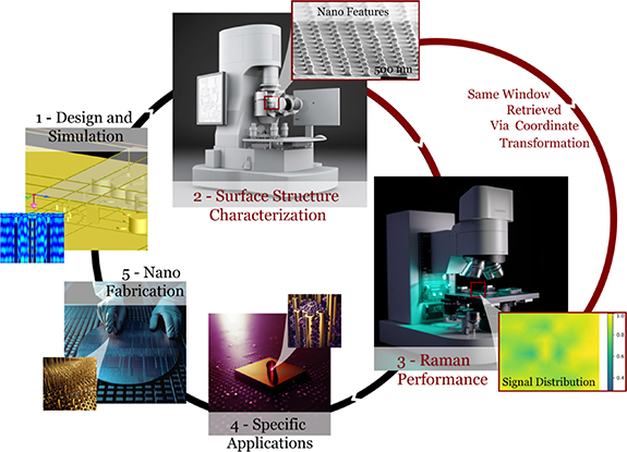
In this paper, we aim to explore the performance metrics of planar SERS substrates and their correlations with the nanostructures' physical characteristics through spectroscopic measurements of the windows that are imaged via a high-resolution SEM. We prepared a planar SERS-substrate characterization methodology and investigated 7 commercial planar SERS substrates from 5 different brands. These substrates were selected to represent a large variety of surface architectures, uniformity levels, structural densities, and fabrication technologies. The primary goal is to interpret SERS performance metrics by examining how they relate to various SERS structures. In this methodology, the substrates are first imaged with a SEM to extract their physical characteristics. SEM was selected as the surface characterization technique considering its accessibility and the nanometer resolution requirements of the substrates. The imaged windows are retrieved with a Raman microscope through coordinate transformation. Spectroscopic measurements are used to calculate the performance metrics of each substrate. The nanostructure's morphology is the most significant contributor to a SERS substrate's performance [5]. Our benchmarking results confirmed the theoretical expectations for the different nanostructures and implied guidelines for better application-specific enhancement. Our methodology and results can encourage a better understanding of the SERS literature as well as better practices for the development, characterization, and application of planar SERS substrates.
2. Results and discussion
2.1. Surface structural features
High-resolution SEM imaging characterized the physical characteristics of the substrates as presented in figure 1. Although SEM offers only two-dimensional information about the morphology of the substrates, it is a fast and accessible approach that can satisfy the resolution requirements of features as small as tens of nanometers. Furthermore, the third dimension can be studied by measurements at an angle. Atomic force microscopy, an alternative to SEM, can provide three-dimensional images. However, this technique suffers from artifacts like enveloping due to narrow but deep crevices and abrupt profile changes [30].

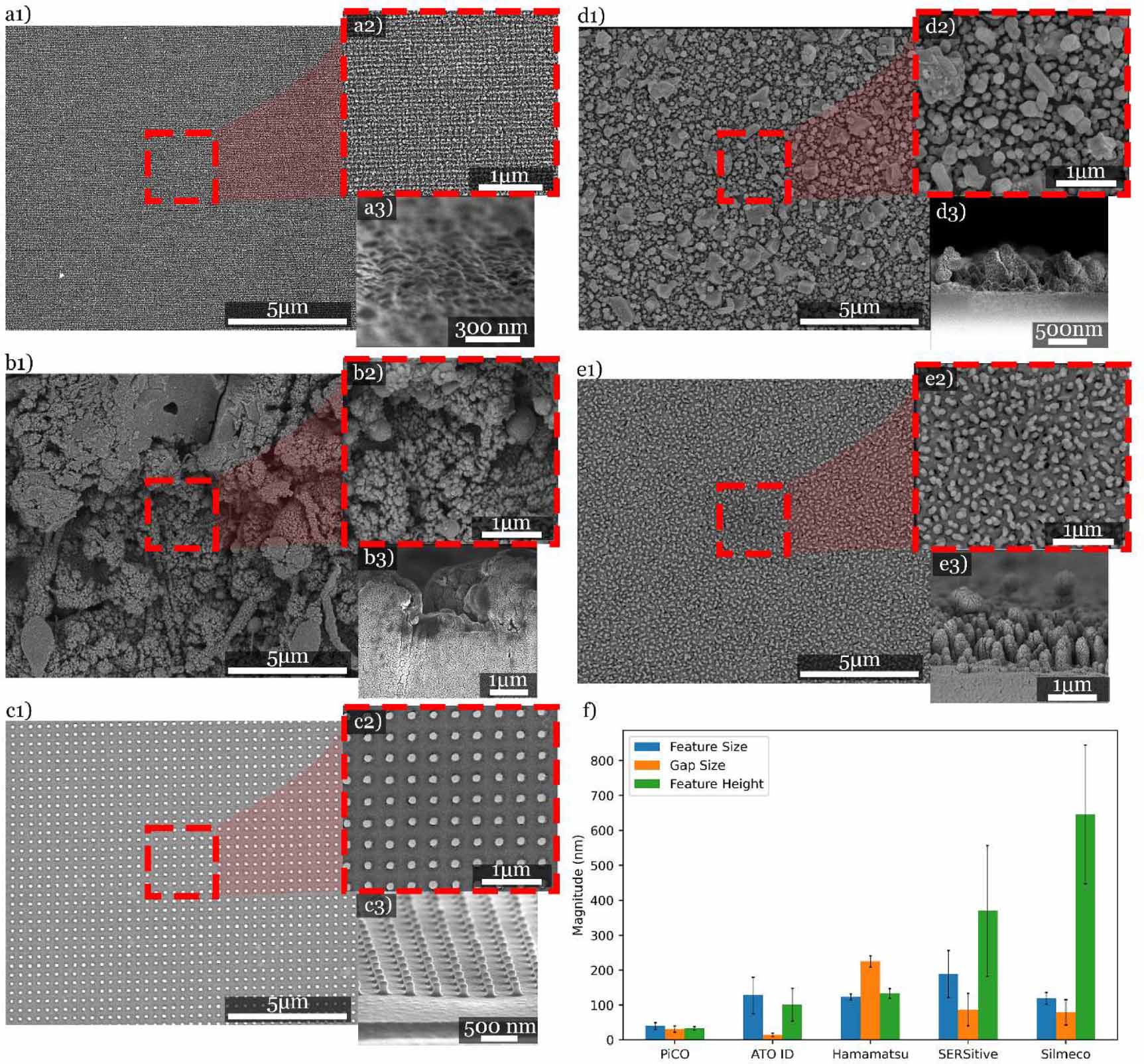
Figure 1. Top-view SEM images of (a1) PiCO Au, (b1) ATO ID Ag, (c1) Hamamatsu Au, (d1) SERSitive Ag, and (e1) Silmeco Au SERS substrates' nanostructures. The dashed red squares (b2)–(e2) highlight a magnified section of the top-view images. Beneath the squares, the polished cross-sections are presented (a3)–(e3). (f) summarizes the characteristics of the substrate types.
Download figure:
Standard image High-resolution imageEach substrate is randomly structured to an extent. For instance, figure 1(a) has a grid-like structure with random feature sizes, making it less random than the randomly deposited nanoparticles in figure 1(d). Thus, the qualitative extent of order or randomness is one of the factors investigated for the SERS substrates here. Moreover, every nanostructure has specific building blocks, here called features, that are primarily responsible for the enhancement. Consequently, the additional factors investigated for the substrates here are the features' lateral size, height, and the size of the gaps between them. Table 1 provides an overview of the mentioned characteristic factors for the investigated SERS substrates. The feature-related factors are visualized in figure 1(f).
Table 1. The summary of the commercial SERS substrates' surface structure characteristics as measured by SEM.
| SERS substrate | Fabrication technology | Feature size (nm) | Gap size (nm) | Feature height (nm) | Structural order | References |
|---|---|---|---|---|---|---|
| PiCO | Nano-transfer printing | 40 ± 10 | 31 ± 9 | 33 ± 5 | Stripe pattern | [31] |
| ATO ID | Femtosecond laser | 128 ± 52 | 14 ± 5 | 101 ± 47 | Random | — |
| Hamamatsu | Nanoimprinting | 123 ± 9 | 225 ± 16 | 133 ± 14 | Dot array | — |
| SERSitive | Electrodeposition | 189 ± 67 | 87 ± 46 | 370 ± 187 | Random | — |
| Silmeco | Reactive ion-etching | 119 ± 17 | 79 ± 36 | 646 ± 199 | Random | [32] |
Each substrate was fabricated using a different nanofabrication technology with a different structure and detection strategy. PiCO uses nano-transfer printing technology to create 3D structures using nanowires in silicon; the structure is then coated with gold and nanoparticles for increased sensitivity [31]. PiCO's strategy is to make the structures as small and ordered as possible aspiring to achieve high and stable enhancement. The nanoparticle decoration augments the substrate's enhancement capability. As presented in figure 1(a), this substrate has randomly shaped features and gaps arranged in a grid-like structure. The features have a mean lateral size of 40 ± 10 nm, gap size of 31 ± 9 nm, and height of 33 ± 5 nm. The smallest feature size is around 10 nm. Furthermore, ATO ID fabricates its SERS substrates in soda lime glass using a femtosecond laser nanofabrication technique resulting in stochastic structures that can be seen in figure 1(b). The substrate's structure can be viewed as a random distribution of small features in a roughened landscape. ATO ID's detection strategy is that the variety of feature sizes makes the substrate suitable for a wide range of excitation wavelengths. The small features can be as small as tens of nanometers and have a mean lateral size of 128 ± 52 nm, gap size of 14 ± 5 nm, and height of 101 ± 47 nm. The landscape's lateral features can be as large as several micrometers with a mean lateral size of 1504 ± 622 nm and an average height of 2371 ± 514 nm. It is important to note that the reported sizes are merely average values and that this structure is highly random. Moreover, Hamamatsu uses nanoimprint technology to create a highly ordered nanopillar array in silicon as viewed in figure 1(c). These highly ordered and repeatable structures can stimulate signal stability and repeatability. The mean lateral feature size is 123 ± 9 nm, the mean feature height is 133 ± 14 nm, and the mean gap size is 225 ± 16 nm. In comparison to the other substrates, the structure of this substrate is more uniformly ordered. Furthermore, SERSitive creates its SERS substrates through the electrodeposition of metallic nanoparticles on ITO glass. Figure 1(d) shows the random shapes and sizes of the deposited nanoparticles. The largest particles are micrometer-sized agglomerates, while the smallest ones are tens of nanometers. SERSitive's average lateral feature size is 189 ± 67 nm with a mean gap size of 87 ± 46 nm and feature height of 370 ± 187 nm. Beware that this substrate's structure is random and that these numbers are only an average quantification of its feature's dimensions. Finally, the 'SERStrates' of Silmeco are fabricated in silicon using maskless reactive ion etching featuring leaning pillars [32]. Silmeco's detection strategy is to increase the features' height in addition to minimizing the lateral feature sizes, to enable more hotspots. Silmeco promotes molecule trapping via its pillar-leaning feature. Figure 1(e) shows this substrate's randomly positioned pillars, with some conjoined by the coating. This substrate's pillars have a mean size of 119 ± 17 nm, gap size of 79 ± 36 nm, and height of 646 ± 199 nm.
2.2. SERS performance
BPEs four characteristic Raman peaks, 1020, 1198, 1606, and 1636 cm−1 are used to investigate the SERS performance metrics [33]. The measured SERS spectra and the peaks of interest of BPE are shown in figure 2. The peaks' slight deviation from the mentioned values, in the order of a few data points, is an artifact of averaging the map's spectra; point to point variations can add up to a peak maximum slightly shifted. Furthermore, the substrates that contained silver, e.g. ATO ID Ag, showed extra peaks due to silver's reactive nature, e.g. oxidation. However, these peaks are usually smaller than 100 counts and will be subdued with a strong analyte signal as in Silmeco Ag's case. Furthermore, the signal-to-noise ratio can be seen from the noise that is superimposed on the spectra; Silmeco Ag's spectrum is much smoother compared to ATO ID Ag as the signal is much stronger than the noise.

Figure 2. Raw SERS spectra of 50 µM BPE for the 5 substrate types averaged over a 15 µm × 15 µm map i.e. 81 spectra. Vertical dashed blue lines represent the peaks of interest.
Download figure:
Standard image High-resolution imageThe first performance metric is signal stability which is the most important characteristic of a detector used for quantification [34]. Different surface morphologies can lead to different spatiotemporal signal instabilities depending on the number of hotspots covered with the exciting laser. Expanding the illuminated area on a structure increases the number of hotspots producing the signal. Thus, the signal's variations are averaged over a larger number of hotspots, and as such the signal becomes more reproducible. The same reasoning applies when comparing different structures: if a structure's number of hotspots is more than another's under the same illumination, its signal is relatively more stable. For instance, a 1 µm2 area sees a lot more variation in the case of ATO ID (figure 1(b)) compared to PiCO (figure 1(a)). The signal stability over time and area is imperative for quantitative analyses or SERS imaging, while a strong signal suffices for identification alone. To study the spatial signal stability, several maps were measured across the SERS active area. An instability metric was introduced as the STD of a characteristic peak scaled by its intensity over the map, i.e. a modified definition of the CV. To calculate this metric for a map, find the STD over the map and divide it by the map's average intensity. Figure 3(a) demonstrates the instability of the studied substrates for the characteristic peaks of BPE. The substrate with the highest relative structural order, Hamamatsu, has the lowest spatial instability, equal to 0.09% with a 0.01% map-to-map variation for the 1636 cm−1 peak. Silmeco Au comes second in stability but has a higher map-to-map variation than Hamamatsu because of the random position and height of its pillars. PiCO, Silmeco Ag, and SERSitive substrates have the same stability, although PiCO's structural order and features' dimensions give its map-to-map variation an edge over the more randomly ordered structures. Finally, ATO ID has the highest instability and map-to-map variation among the studied substrates. This can be associated with this substrate's random structure and relatively lower hotspot density. Moreover, temporal instability is demonstrated by the signal variations of a point over time. Figure 3(b) visualizes this instability as the CV for the different substrates. The CV values were averaged over the center points of the 3 measured windows. Although this is a temporal study, it inherently has traces of spatial instability due to the averaging. Nonetheless, the temporal instability was found to have an inverse relationship with the signal's strength. Moreover, BPE's peaks of interest have the same trend except for 1020 cm−1, as seen in figure 3. This peak is the weakest of the four and its signal-to-noise ratio is close to unity. This can be seen better when considering figure 2 and comparing ATO ID Ag to the other substrates. As this substrate's signal-to-noise ratio is relatively smaller and closer to the noise of the measurements, it is less stable over space and time.

Figure 3. The instability of the SERS signal over (a) the measured maps and (b) single point measurements for the 7 SERS substrates studied for a BPE concentration of 20 μM. The error bars demonstrate the coefficients of map-to-map variation.
Download figure:
Standard image High-resolution imageUnderstanding the spatiotemporal limitations of a SERS substrate helps with its further development or applications. To elaborate, PiCO has a better structural order compared to SERSitive, but by increasing the beam spot to spatially average more structural variations, SERSitive can have similar signal stability. However, that limits this SERS substrate's minimum resolution for SERS imaging applications. The temporal instabilities can be averaged out by longer acquisition times. Despite that, an advantage of using SERS substrates is faster acquisitions but large temporal variations hinder the minimization of the measurement time.
The enhancement capability of the substrates can be discussed through their EF. A higher EF translates to a stronger signal and higher sensitivity. Thus, the substrates' enhancement capability follows the same logic as the signal's spatiotemporal stability; different structural features lead to different enhancements. Furthermore, the higher the number and strength of the hotspots in the investigated area, the higher the enhancement. Figure 4 highlights the lateral distribution of EF values that are maximum normalized over the SEM-measured windows for the different substrate types. Hamamatsu which had the most ordered structure (figure 1(c)) has the highest lateral EF homogeneity i.e. lowest CV over the surface. The maximum EF for this substrate in the measured window is 1.2 × 10⁶ ± 3.5 × 10⁴, as seen in figure 4(f). Silmeco and SERSitive come second and third in EF's spatial homogeneity while they are first and second in maximum EF, respectively. PiCO and ATO ID have the highest spatial variation and the lowest EF within the substrates studied. Table 2 summarizes the statistics of the maps' EF values for two analyte concentrations.
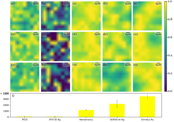
Figure 4. Maximum normalized EF maps of the 3 SEM measured windows of (a1)–(a3) PiCO Au, (b1)–(b3) ATO ID Ag, (c1)–(c3) Hamamatsu Au, (d1)–(d3) SERSitive Ag, (e1)–(e3) Silmeco Au for the 1636 cm−1 BPE peak and 20 μM concentration. The bar plot, (f), shows the absolute maximum EF averaged over the 3 maps. The error bars show the map-to-map variation of the maximum EF. The vertical axis has a factor of 1000.
Download figure:
Standard image High-resolution imageTable 2. An overview of the maps' EF values' descriptive statistics calculated for the 1636 cm−1 peak of BPE. The errors represent the map-to-map variation. The reported number in this table have a factor of 1000.
| 1 μM | 20 μM | |||||
|---|---|---|---|---|---|---|
| SERS substrate | Mean (a.u.) | Maximum (a.u.) | STD | Mean (a.u.) | Maximum (a.u.) | STD (a.u.) |
| PiCO Au | 266 ± 20 | 619 ± 9 | 140 ± 4 | 55 ± 7 | 79 ± 8 | 10 ± 1 |
| ATO ID Ag | 165 ± 39 | 1029 ± 183 | 358 ± 42 | 18 ± 10 | 74 ± 32 | 20 ± 2 |
| Hamamatsu Au | 2878 ± 111 | 4111 ± 192 | 541 ± 22 | 963 ± 7 | 1173 ± 35 | 87 ± 9 |
| SERSitive Ag | 1145 ± 106 | 2911 ± 520 | 710 ± 133 | 1450 ± 442 | 2185 ± 645 | 259 ± 110 |
| SERSitive AgAu | 2449 ± 342 | 4917 ± 770 | 953 ± 184 | 190 ± 3 | 393 ± 42 | 67 ± 14 |
| Silmeco Au | 7261 ± 1358 | 11 737 ± 1345 | 1677 ± 157 | 2669 ± 216 | 3466 ± 314 | 362 ± 83 |
| Silmeco Ag | 17 143 ± 4816 | 30 498 ± 9567 | 4046 ± 821 | 2455 ± 676 | 3740 ± 859 | 463 ± 85 |
The features' aspect ratio is found to be correlated to the SERS structures' hotspot density. The maximum EF (figure 4(f)) increases with the aspect ratio of the features. Furthermore, the CV over the surface was found to be correlated to the error bars representing the map-to-map variation of the maximum EF. While PiCO and ATO ID have a low EF in all maps and consequently a small error bar, Hamamatsu, SERSitive, and Silmeco's CV follow their structural order. In addition, silver's superior plasmonic activity with respect to gold can be seen by comparing the EF of Silmeco Ag vs Au. Another interesting behavior regarding SERS material is the concentration range in which the signal is enhanced. Comparing the SERSitive materials, one can see that SERSitive AgAu has a better EF than SERSitive Ag for 1 μM concentration and vice versa for 20 μM concentration. This behvaior's origin can be the additional Au nanoparticles in SERSitive AgAu, consequently the denser structure. A denser structure performs better in a lower concentration due to its higher number of hotspots. Because of SERSitive Ag's lower structural density and stronger hotspots, the intensity might be weaker for a low analyte concentration but increases more rapidly as the concentration increases. The relatively low intensity count for SERSitive AgAu in figure 2 despite the 50 μM analyte concentration arises from the same material-related behavior. Moreover, by changing the analyte from BPE to crystal violet with a 1 μM concentration, the maximum EF for Hamamatsu Au and Silmeco Ag are 6.7 × 10³ ± 500 and 3 × 10⁶ ± 6.3 × 10⁵ respectively. It is also important to note that baseline correction strongly affects the results presented here. Without baseline correction, the maximum EF becomes 6.6 × 10⁵ ± 2 × 10⁴ and 1.7 × 10⁷ ± 1.4 × 10⁶, respectively for Hamamatsu Au and Silmeco Ag. To summarize, EF values can be increased by the choice of the performance analyte, baseline correction, analyte concentration, etc. However, this does not mean that the substrate's SERS performance has improved or is better in comparison. The SERS results presented here are not comparable to the commercial substrates' respective publications as the same methodology has not been used here. Finally, the reported performance is specific to the settings mentioned in subsection 3.2. Deviating from these settings could change the reported numbers, as illustrated in table 2.
An advantage of signal enhancement is the resulting improvement in detection sensitivity calculated through calibration plots of the analyte's characteristic peaks. To make a calibration plot, a wide concentration range is favorable as it encourages the inclusion of saturation and below-sensitivity concentrations. When the availability of analyte molecules is below the sensor's sensitivity, no peak shows up in the spectrum. The corresponding point in the calibration plot will be close to zero until the concentration is raised above the sensor's sensitivity and peaks start showing up. Then, the peak intensity will increase linearly with increasing concentration until the number of analyte molecules starts hindering the signal. From that point on, the changes in peak intensity become nonlinear. The rate of the changes becomes smaller as well i.e. the signal saturates. To summarize, the calibration plot's trend starts from almost zero, raises nonlinearly, becomes linear for a range of concentrations, and finally nonlinearly raises to saturation. This is a sigmoidal behavior. As demonstrated earlier, the spatial instability of a SERS substrate can be high, leading to a different concentration range for which the peak's intensity changes linearly. Hence, fitting a sigmoid function to the calibration plot can help to seek the linear range automatically. Figure 5(a) shows how fitting a sigmoid function to the calibration plot with a wide concentration range could help with the selection of the data points for LOD calculations. The center of the fitted sigmoid function indicates the center of concentrations for which the peak intensity changes linearly. Therefore, seven concentrations were selected in the vicinity of the sigmoid fit's center. Although two points are sufficient to fit a line, seven points are taken in the interest of accuracy. The concentrations were selected symmetrically around the sigmoid fit's center. If the center was closer than three points to the starting concentration, then the first seven concentrations would be selected for the calibration plot. The line fitted to the selected concentrations was then used to calculate the LOD, as shown in figure 5(b).

Figure 5. LOD was found using (a) an extended-range calibration plot with a sigmoid fit, then, (b) a calibration plot with the selected points, resulting in LOD values for the 4 characteristic peaks of BPE. (c) The minimum LOD value averaged over the 3 maps for each substrate type. The error bars show the map-to-map variation of the LOD. The example calibration plots brought here are for 1636 cm−1 BPE peak using a Hamamatsu substrate.
Download figure:
Standard image High-resolution imageThe minimum LOD values for the investigated substrates are presented in figure 5(c). Silmeco Ag has the lowest LOD of 0.18 ± 0.19 μM and a LOQ of 0.59 ± 0.64 μM. Moreover, Hamamatsu has the most stable results, as seen in figure 5(c)'s error bars. The detection sensitivity is inversely related to the EF results (figure 5(f)), as expected. Furthermore, the 1020 cm−1 minimum LOD is noticeably different compared to that of the other 3 peaks. This can be explained by the fact that 1020 cm−1 marks the weakest of the four characteristic peaks. Therefore, it might be more unstable compared to the other peaks. Furthermore, a statistical overview of the maps' LOD values is provided in table 3. LOQ differs from LOD by only a factor, thus, everything discussed for LOD applies to LOQ as well.
Table 3. LOD and LOQ of the 1636 cm−1 characteristic peak of BPE for the investigated SERS substrates. The errors represent the map-to-map variation.
| LOD (nM) | LOQ (nM) | |||||
|---|---|---|---|---|---|---|
| SERS substrate | Mean | Min | STDa | Mean | Min | STD |
| PiCO Au | 4323 ± 2068 | 343 ± 49 | 3675 ± 1247 | 13 712 ± 6104 | 1145 ± 162 | 11 044 ± 2785 |
| ATO ID Ag | 12 927 ± 866 | 610 ± 462 | 9715 ± 391 | 26 258 ± 818 | 2033 ± 1540 | 12 047 ± 393 |
| Hamamatsu Au | 900 ± 8 | 210 ± 37 | 567 ± 86 | 3000 ± 26 | 700 ± 123 | 1890 ± 286 |
| SERSitive Ag | 927 ± 526 | 90 ± 51 | 749 ± 498 | 3090 ± 1754 | 298 ± 170 | 2496 ± 1661 |
| SERSitive AgAu | 1693 ± 695 | 40 ± 9 | 2674 ± 1404 | 4770 ± 1771 | 135 ± 31 | 6989 ± 3329 |
| Silmeco Au | 307 ± 142 | 18 ± 5 | 396 ± 270 | 1025 ± 472 | 59 ± 17 | 1321 ± 899 |
| Silmeco Ag | 178 ± 192 | 6 ± 5 | 224 ± 225 | 593 ± 641 | 19 ± 18 | 748 ± 749 |
3. Methods and materials
3.1. Materials
Au 3D-Connected Nanoparticles (PiCO), Randa S—Ag (ATO ID), J12853—Au (Hamamatsu), S-Silver and S-AgAu (SERSitive), and Ag and Au SERStrate (Silmeco) SERS substrates were acquired directly from their producers. 50 nm gold/silver-coated coverslips (AU.0500 & AG.0500) were purchased from Platypus Technologies. Furthermore, BPE (C12H10N2, B52808) and crystal violet (C25H30ClN, C0775) were purchased from Sigma-Aldrich.
3.2. Characterization methods
SEM was carried out using a Nova NanoSEM 450 (FEI). To view the height of the substrates' nanostructures, a cross-section of the substrates was polished with a 6 kV Ar-ion for 3 h using an IB-09010CP (Jeol). The polished cross-sections were recoated with 8 nm gold using a sputter coater (Balzers). The images were acquired using a through-the-lens detector in immersion mode (high resolution) with a landing energy of 5 kV using a stage bias of 3 kV (beam deceleration) and an aperture of 40 µm.
An InVia spectrometer (Renishaw) coupled to a DM2700 optical bright-field microscope (Leica) was used for the Raman measurements. The 785 nm (Diode-pumped solid-state laser—Renishaw) excitation wavelength, which is commonly used in biosensing applications [35], was chosen for these measurements. Furthermore, the selected SERS substrates are optimized for 785 nm excitation. An N PLAN 20X/0.4 objective (Leica) was used to deliver a power of 234 μW across a beam spot of 2.5 μm diameter to the sample for an exposure time of 0.5 s for SERS and 50 s for spontaneous Raman. The collected light was diffracted onto a Centrus CCD detector (Renishaw) using a 1200 lines mm−1 grating. The spectral range of interest was chosen to be 614–1720 cm−1 with a spectral resolution of 1 cm−1. This range includes the strongest peaks of the performance analytes.
3.3. Data acquisition and analysis
Three points were chosen to characterize the surface features of each SERS substrate. Their 20000X and 80000X magnified SEM images as well as their coordinates were recorded. The images had 14.9 μm and 3.73 μm horizontal field width, accordingly. The measured feature sizes were determined using ImageJ software [36]. The reported sizes are averaged over 40 randomly selected features in images of different points. Moreover, three additional coordinates were recorded in the corners of the substrates' active area, allowing for coordinate system transformation when the substrates are moved to the Raman microscope. Furthermore, a 90° SEM mount was used to image several points of the polished cross-section for each substrate.
Via the Raman microscope, the three corner points were retrieved and their coordinates were recorded. As the coordinates of the same corner points are available in both coordinate systems, the SEM-imaged points can be found in the Raman microscope's coordinate system within 1.56 ± 0.60 μm. Every transformed point was measured for 2.5 s with 0.5 s steps, for each analyte concentration. Then, a 15 μm × 15 μm map with 2 μm steps corresponding to the 20000X magnified SEM image was measured. To validate the coordinate transformation between the microscopes, a 1 μm pitch grid was printed on fused silica using a Photonic Professional GT2 (Nanoscribe). Orthogonal markers, including the one shown with a red arrow in figure 6, were used in the grid, and their coordinates were recorded as the common coordinate system between the two microscopes. A target, shown by a red circle in figure 6(a), was recorded to be retrieved under the Raman microscope. The coordinate transformation between the microscopes was calculated using the correlation module of WiRE (Renishaw). The transformation error, 1.56 ± 0.60 μm for the 20X objective, was calculated as the distance from the transformed coordinate to the target's actual center in figure 6(b).

Figure 6. A grid with a 1 μm pitch as viewed under the (a) SEM and the (b) Raman microscope. The red arrows show one of the three coordinate points while the red circle marks the target.
Download figure:
Standard image High-resolution image
Before the analyte deposition, the substrates' surfaces were cleaned of any organic molecules using a PiezoBrush plasma pen (Relyon) with a nearfield nozzle. This technique also increases surface affinity to ethanol, the preferred solution for its rapid evaporation and distribution over the nanostructures. Thus, depositing a small aliquot of the analyte's ethanol solution, here 1 μl for a 9 mm2 projected area, improves the delivery of its molecules to the hotspots and hinders the coffee ring effect. Drying in vapor-saturated chambers can be a cumbersome alternative. Drop-casting was used to apply the analytes, BPE and crystal violet, in a dilution series of 0.1–1 μM (0.1 μM step), 2–20 μM (1 μM step), and 30–50 μM (10 μM step). The SERS measurements were done after the deposited aliquot dried out. Finally, the spontaneous Raman measurements were done inside 20 μl droplets on 50 nm metal-coated coverslips (AU.0500 & AG.0500 Platypus Technologies). The measurement settings were the same as SERS but with a 50 s acquisition time, instead of 0.5 s, chosen based on the evaporation rate of ethanol.
The spectra's baselines were subtracted using asymmetric least squares [37], ensuring that the intensity variations do not come from the fluorescent background. The STD, EF, and LOD were calculated on the four strongest characteristic peaks of the analyte individually. The CV over space was calculated over the 81 spectra measured in the 15 μm × 15 μm maps. The CV over time was calculated over the 5 spectra measured in the same spot over 2.5 s. The former shows spatial intensity variations, while the latter represents the peaks' time-dependent instability. The most widely used definition of the SERS EF [38], shown in equation (1), was used here.

To elaborate, ISERS is the SERS peak intensity, NSERS is the number of molecules on the surface contributing to the SERS signal, INR is the same peak's intensity in the spontaneous Raman spectrum, and NNR is the number of molecules in the laser's collection volume when measuring spontaneous Raman. As minimum coffee-ring effects occur due to surface pretreatment, the signal changes primarily result from the nanostructures' architecture. The beam spot's area, calculated using the airy-disk formula, was used to determine NSERS assuming uniform molecular distribution. However, the same justification does not apply to the coffee rings on a nonstructured surface. Consequently, the INR was measured in a homogeneous solution. Ethanol does not emit fluorescence with near-infrared excitation, nor does it have overlapping Raman peaks with the analytes. Therefore, the main contribution to INR comes from the homogeneously distributed molecules in the collection volume, calculated as the beam spot's area multiplied by the confocality height. The full width at half-maximum of a silicon target's 520 cm−1 peak in a height scan was taken as the confocality height. Finally, equation (2) was used to calculate LOD based on the STD of the signal without analyte (σ) and the slope of the calibration curve (S) [39]. σ was taken to be the time-STD of the peak intensity without any analyte deposited on the substrate. The LOQ has the same formula with a factor of 10 instead of 3.3.

4. Conclusions
SERS is receiving great attention due to its sensitive identification capabilities and integrability. Many of the SERS research articles discuss novel fabrication techniques or applications. However, the comparability of the reported performance metrics, such as EF and LOD, is minimally explored. Here, we have introduced a planar SERS substrate benchmarking methodology including two parts, characterization of the nanostructures and SERS performance analysis. Seven commercial planar SERS substrates from 5 different brands were studied using this methodology. The first part analyzed the structures based on their order and the size of their features, finding Silmeco to have the highest aspect ratio and Hamamatsu to have the most ordered structure. The second part demonstrated a direct correlation between the aspect ratio of the nanostructures' features and the maximum EF achievable. Silmeco Ag was found to have the highest EF and consequently the lowest LOD. Furthermore, the nanostructures' order was shown to affect the spatiotemporal signal stability leading to variations in all the performance metrics. Hamamatsu, with a highly ordered array of pillars, has the least variation in its performance metrics. From the correlations of structure and performance, one can infer that hotspot density and uniformity can be used to estimate SERS performance.
Although this methodology can find the SEM-measured window within 1.56 ± 0.60 μm, higher magnification objectives will improve the coordinate transformation and could facilitate the point-to-point mapping of the results. Therefore, EF maps with higher resolutions can pinpoint the specific features that are performing better within the limits of diffraction and scattering. Additionally, a combination of heating and air flow could refine the homogeneity of the analyte distribution over the substrates. We will try to include these points in our future work regarding the development of planar SERS substrates for biomedical applications.
Our results show that the reported performance metrics can be highly sensitive to the specific measurement settings or assumptions in the calculations e.g. optical setup, post-measurement processing of signals, and choice of the performance analyte. Therefore, a conclusive way to investigate a SERS substrate's performance is to benchmark it against a commercially available SERS substrate as shown here. Furthermore, this benchmarking methodology can guide the development and application of planar SERS substrates in an easy and accessible way. For instance, if one were to use SERS imaging to follow the evolution of an abundant metabolite, PiCO is a potentially better option due to its relatively higher homogeneity compared to SERSitive, although SERSitive is multiple times more sensitive. Moreover, the methodology is not limited to SEM; any other characterization system e.g. atomic force microscopes can replace or be combined with SEM. Finally, the findings presented here do not support any of the investigated substrates as superior or inferior. Our objective is to present how an analytical study can help to understand the limitations and strengths of a SERS substrate for a specific application or the next stages of its development.
Acknowledgments
The authors acknowledge Funding by the European Union within the Horizon Europe Program, under the EIC Pathfinder Project 'VortexLC', Grant Agreement No. 101047029. This work was also supported in part by the Methusalem and Hercules foundations and the OZR of the Vrije Universiteit Brussel (VUB).
Data availability statement
The data cannot be made publicly available upon publication because they are not available in a format that is sufficiently accessible or reusable by other researchers. The data that support the findings of this study are available upon reasonable request from the authors.
Conflict of interest
The authors declare that they have no competing interests.
Authors' contributions
Mehdi Feizpour: Conceptualization, Data curation, Formal analysis, Investigation, Methodology, Resources, Software, Validation, Visualization, Writing—original draft, Writing—review & editing; Qing Liu: Supervision, Writing—review & editing; Tom Van der Donck: Resources; Hugo Thienpont: Funding acquisition; Wendy Meulebroeck: Resources, Supervision, Writing—review & editing; Heidi Ottevaere: Resources, Supervision, Writing—review & editing, Funding Acquisition.