

Abstract
The quantum yield in silicon has previously been assumed to be of significance only in the ultraviolet spectral range. Due to the low internal losses of induced-junction silicon photodiodes and their predictability it is possible for the first time to make more accurate estimation of the quantum yield. We report on measurement of quantum yield in induced-junction silicon photodiodes. The results show that the quantum yield can be larger than unity even at wavelengths around 450 nm. A model of the quantum yield has been fitted to the experimental data and can be implemented in the spectral responsivity models to maintain high accuracy predictability to around 160 ppm down to 360 nm.
Export citation and abstract BibTeX RIS

Original content from this work may be used under the terms of the Creative Commons Attribution 4.0 license. Any further distribution of this work must maintain attribution to the author(s) and the title of the work, journal citation and DOI.
1. Introduction
Photodiodes are the workhorses in radiometry and photometry and are extensively used as transfer standard detectors. Silicon photodiodes are especially interesting as they are sensitive over the visible spectral range, are highly uniform, fast, fairly stable, cheap and predictable. It is beneficial to have predictable standards as this enables independent realisations of spectral response with silicon photodiodes and fewer calibration points when used as transfer standard detectors only.
The quantum yield  is defined as the ratio of the number of generated electron–hole pairs and the number of absorbed photons in a semiconductor photodiode. It is one of the quantities determining the spectral responsivity
  of a photodiode which is defined as the ratio of the photocurrent and the incident radiant power generating this photocurrent. The 3D simulation model used for the prediction of the spectral responsivity does not include quantum yield. Thus, the knowledge of the quantum yield is necessary to accurately model the spectral responsivity of a predictable quantum efficient detector (PQED) independently.
The quantum yield equals unity if the energy of the absorbed photon is between one and two times the band gap energy Eg. For silicon photodiodes with a band gap energy of 1.12 eV this is the wavelength range from about 550 nm to 1100 nm.
The quantum yield can exceed unity if one of the generated charge carriers, the electron or the hole, has enough energy to create a second electron–hole pair via impact ionisation. To achieve impact ionisation the photon energy must exceed 2Eg. However, because of the requirement of simultaneous energy and momentum conservation in combination with the band structure of silicon, a quantum yield above unity occurs only for photon energies larger than 2Eg. The longest wavelength at which a quantum yield above unity has been derived for silicon from experimental data varies between 365 nm and 415 nm [1–3] which correspond to photon energies of 3Eg and 2.6Eg, respectively.
At high photon energies above 12.4 eV, which corresponds to wavelengths shorter than 100 nm, the quantum yield in silicon seems to be proportional to the energy of the absorbed photon [4].
The quantum yield can be calculated from the measured spectral responsivity. This, however, requires a detailed knowledge of the reflectance losses and the internal losses of a photodiode. Whereas reflectance losses can be measured or calculated with low uncertainty, the estimation of the internal losses is difficult as it requires either the knowledge of quantum yield itself or a sophisticated physical model of the internal losses.
Models of the quantum yield are so far semiempirical and suffer from free parameters [3, 5] and inaccurate experimental data and are up to date far away from being applicable at the 100 ppm level. This is crucial for the attempt to establish a new primary detector standard for radiant power measurements, called PQED [6, 7]. On the other hand, the concept of the PQED equipped with specially designed induced-junction silicon photodiodes allows the prediction of the internal losses of the photodiode and thus, for the first time makes it possible to precisely estimate the quantum yield.
In the following, the determination of the quantum yield in induced-junction silicon photodiodes is described and a model for the quantum yield in the wavelength range from 360 nm to 500 nm is developed.
2. Determination of the quantum yield
The external quantum efficiency  of a semiconductor photodiode is given by

The parameters  and
and  describe the external losses due to the reflectance of the photodiode detector and the internal losses due to recombination of charge carriers generated by the incident photons, respectively. Equation (1) can be rearranged for the determination of the quantum yield:

Here, it is assumed  and
and  .
.
 can be calculated from the measured spectral responsivity
  via
via
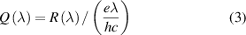
where e is the elementary charge, h is the Planck constant, c is the speed of light in vacuum and λ is the vacuum wavelength.
The external losses  can be measured and/or calculated. An experimental determination of the internal losses
  at wavelengths where the quantum yield
  is unknown is difficult as an experimental separation between both is not possible. Thus,
  must either be calculated or extrapolated from a wavelength region where the quantum yield is known to be equal unity. For both options, a model is required to obtain an estimation of the internal losses with sufficiently low uncertainty.
In the following, the quantum yield of induced-junction silicon photodiodes of a PQED will be determined according to equations (2) and (3).
3. The PQED
The PQED is based on specially designed silicon photodiodes, the induced-junction photodiodes, and a sophisticated physical model of the photodiode's internal losses allowing for the prediction of the photodiode's spectral responsivity with low uncertainty. The induced-junction photodiodes are made of high purity silicon wafer with a very low doping level of about 2·1012 cm−3. Usually, the p–n junction is achieved by doping the silicon crystal with impurities which creates defects in the semiconductor crystal. These defects increase the recombination of generated charge carriers and thus increase the internal losses of a photodiode. The responsivity is also highly sensitive to the doping profile given by the doping level and depth. The large number of defects in a p–n junction and sensitivity to the unknown doping profile makes it difficult to accurately predict the internal losses by a physical model. To avoid these disadvantages, the p–n junction of an induced-junction photodiode is generated by a surface charge trapped in the passivation layer of the silicon [8]. Thus, the purity of the silicon is conserved resulting in low internal losses and the possibility to predict these losses with high accuracy [9]. The concept of the PQED requires the knowledge of the quantum yield, and because of that, the PQED enables the investigation of the quantum yield because of the predictability of the low internal losses.
Two PQEDs [6, 7] studied here are each constructed from two induced-junction silicon photodiodes arranged in a wedge trap configuration. The windowless photodiodes (figure 1) were manufactured in the second processing round of the iMera Plus JRP 'qu-Candela'. They differ in the thickness of the silicon dioxide layer, being 220 nm and 301.4 nm thick in case of PQED_thin and PQED_thick, respectively. The angle between the photodiodes is 11.25° yielding nine reflections of an incoming laser beam if the PQED is aligned so that the reflected beam and the incident one are collinear.

Figure 1. Picture of an induced-junction photodiode module used in the construction of PQED.
Download figure:
Standard image High-resolution image4. Measurement of the spectral responsivity
The spectral responsivity of the two PQEDs was measured in the wavelength range from 360 nm to 531 nm for p-polarised laser radiation. The measurements were performed at the laser-based cryogenic radiometer facility of the Physikalisch-Technische Bundesanstalt (PTB). The facility is equipped with a common Brewster window which means that cryogenic radiometer and PQED under test are irradiated through the same window. Thus, the correction for and the uncertainty contribution from the Brewster window transmittance can be avoided. The detector cavity of the cryogenic radiometer and the PQED are equipped with input apertures with the same diameter of 7 mm and were irradiated at the same position with respect to the laser beam. Thus, the uncertainty contribution arising from the scattered radiation around the laser beam is reduced. A relative standard uncertainty of spectral responsivity between 30 ppm and 50 ppm has been achieved. Figure 2 shows the external quantum efficiency  calculated from the measured spectral responsivity according to equation (3) and we observe that the external quantum efficiency differs by up to 600 ppm between the two PQEDs.

Figure 2. External quantum efficiency  as a function of wavelength for two PQEDs with different passivation layer thickness.
Download figure:
Standard image High-resolution imageIn order to isolate the influence of quantum yield we need to decompose the influence of each of the loss parameters as will be discussed in the following chapters.
5. External losses due to reflectance
The estimation of the external losses due to reflectance of the PQED is based on the transfer-matrix method [10] taking into account the photodiode layered structure and material parameters combined with the multiple reflections between the photodiodes. Material parameters and layer thicknesses are taken from the literature [11, 12] or measured directly, e.g. using ellipsometry for oxide thickness [13]. Each parameter's uncertainty is taken into account to calculate the combined reflectance uncertainty. In addition, a photocurrent ratio between the two photodiodes in the trap structure was used to confirm that the used parameters are valid and the PQED is properly aligned relative to linearly polarised light [14]. The measured and modelled ratios agreed within the expanded (k = 2) uncertainties, which were 3.4% to 4.6% for modelled values, depending on wavelength. The uncertainties of the measured ratios were limited with electrical measurement capabilities and were in the order few tens of ppm. Difference between measured and modelled ratios were below 2% at all used wavelengths. In this way we estimated the reflectance losses (equations (1) and (2)) of the two different PQEDs.
6. Internal losses due to recombination
The internal losses ( ) are predicted using Genius simulation software from Cogenda [9]. The calculated
  of qu-Candela PQED photodiodes depends on parameters like oxide fixed charge (
 ), surface recombination parameter (
 ), bulk doping concentration (
 ) and bulk lifetime (
 ). When sufficiently biased
  , at short wavelengths below 800 nm, is mainly limited by the
  parameter which is directly proportional to the number of interface defect states. In the prediction of
  we have kept typical model parameters known from the manufacturing of the photodiodes and fitted the
  parameter to match the measured
  value at 531 nm, because it is assumed that the
  is equal to 1 at this wavelength. Uncertainty estimates for
  at short wavelengths were found by recalculating a new
  with a 30 ppm offset in the
  value at 531 nm. That means the
  parameter was fitted to match the 30 ppm offset in the
  value at 531 nm yielding a second value for the
  parameter with associated
  at short wavelengths. The difference between the original fit and second
  is used as the uncertainty in
  . Table 1 shows the parameters used in the estimation of the internal quantum deficiency in each of the two PQEDs. From the calibration point at 531 nm we were now able to isolate the spectrally dependent
  for each of the two PQEDs.
Table 1. Model parameters used for the calculation of the internal losses due to recombination.
| PQED_thin | PQED_thick | |
|---|---|---|
 /cm−2 /cm−2
| 6 × 10¹¹ | 6 × 10¹¹ |
 /(cm s−1) /(cm s−1) | 25.1 × 10³ | 46 × 103 |
 /cm−3 /cm−3
| 2 × 10¹² | 2 × 10¹² |
 /s /s | 3 × 10⁻³ | 3 × 10⁻³ |
7. Quantum yield results
Table 2 shows the results on the measured external quantum efficiency  from measurements against the cryogenic radiometer, external reflectance losses
  and internal fitted and predicted losses
  as well as the quantum yield
  calculated from the first three quantities according to equation (2). In addition, the standard uncertainties of these quantities are stated. For completeness of the table, the calculated quantum yield values from the model are also included and the derivation of these values are explained in the following section. The uncertainty in the estimation of the quantum yield is limited by the propagated uncertainties from the fitted internal losses at 531 nm.
Table 2. Results on external quantum efficiency  , external losses
  and internal losses
  and quantum yield
  together with the standard uncertainties. In addition, the quantum yield ym(λ) estimated by the model is shown in the last column.
| λ/nm | Q(λ) | u(Q(λ)) × 106 | ρ(λ) × 106 | u(ρ(λ)) × 106 | δ(λ) × 106 | u(δ(λ)) × 106 | y(λ) | u(y(λ)) × 106 | ym(λ) model | |
|---|---|---|---|---|---|---|---|---|---|---|
| PQED thick | 395 | 1.001 263 | 30 | 222 | 22 | 1040 | 330 | 1.002 53 | 330 | 1.002 701 |
| 407 | 1.000 687 | 32 | 225 | 16 | 740 | 230 | 1.001 66 | 240 | 1.001 703 | |
| 415 | 1.000 277 | 30 | 211 | 12 | 620 | 190 | 1.001 11 | 200 | 1.001 222 | |
| 425 | 0.999 948 | 30 | 172 | 9 | 490 | 150 | 1.000 61 | 160 | 1.000 797 | |
| 450 | 0.999 723 | 30 | 57 | 4 | 275 | 87 | 1.000 055 | 92 | 1.000 241 | |
| 531 | 0.999 897 | 30 | 0.03 | 0.004 | 95 | 30 | 0.999 993 | 42 | 1.000 000 | |
| PQED thin | 360 | 1.006 535 | 30 | 980 | 170 | 2100 | 1200 | 1.0096 | 1200 | 1.009 356 |
| 395 | 1.001 846 | 30 | 5 | 0.6 | 570 | 330 | 1.002 42 | 330 | 1.002 701 | |
| 407 | 1.001 171 | 40 | 1 | 0.1 | 410 | 230 | 1.001 58 | 240 | 1.001 703 | |
| 415 | 1.000 693 | 30 | 0.4 | 0.04 | 340 | 190 | 1.001 03 | 200 | 1.001 222 | |
| 425 | 1.000 409 | 30 | 0.2 | 0.02 | 270 | 150 | 1.000 68 | 160 | 1.000 797 | |
| 450 | 1.000 058 | 30 | 0.2 | 0.04 | 150 | 86 | 1.000 208 | 91 | 1.000 241 | |
| 476 | 0.999 960 | 30 | 0.8 | 0.2 | 99 | 57 | 1.000 059 | 64 | 1.000 051 | |
| 531 | 0.999 939 | 37 | 8 | 0.8 | 52 | 30 | 0.999 999 | 48 | 1.000 000 |
8. Quantum yield model
The measured quantum yield  was modelled by using the interpolation function taking into account the effects of impact ionisation and electron–phonon scattering on probability of producing secondary electrons as described, e.g. in [3, 15]. The interpolation function used to model quantum yield
  is proposed as
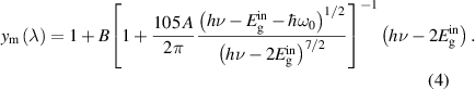
The following symbols and values are used in the interpolation function:
 = 0.551 eV−1 is the only fitting parameter used in equation (4). The parameter B includes effective density of states per unit energy and depends on band structure model used in the energy range studied and may depend on temperature [16]. In the present study, the band structure of silicon was not modelled and, therefore, the parameter B is adjustable in our interpolation function.
 = 5.2 eV3 factor describing relative amounts of scattering by phonon emission and by impact ionisation [15]
 - photon energy of the applied radiation converted from wavelength
 = 0.062 eV, phonon energy [15]
 = 1.123 eV, indirect bandgap of silicon at 298 K [16].
The interpolation function equation (4) includes one free parameter B. At a given temperature, the parameter B is considered as a scaling factor which can include components arising from structure of silicon, e.g. effective density of states.
We have used the factor 2Eg in as a threshold for impact ionisation in silicon, where Eg in is indirect bandgap (Eg in = 1.123 eV at room temperature). This is well in the range of the threshold values from 1.1 eV to 3.1 eV theoretically predicted by several authors, e.g. [17–19].
The estimated quantum yield of the two PQEDs is shown in figure 3. It can be noticed that measured external quantum efficiency and, consequently, reflectance and internal quantum deficiency depend on the PQEDs (table 2). We observe that when correcting for the individual loss parameters of the PQEDs the estimated quantum yield of the two PQEDs differ by 153 ppm or less (see table 2) and agree within their expanded (k = 2) uncertainties in the wavelength range from 531 nm to 395 nm. This is reassuring, as we expect the quantum yield to be a material specific parameter and less sensitive to individual devices. By using our proposed interpolation function equation (4), the quantum yield over the spectral range from 360 nm to 540 nm is calculated and shown with black solid line. The model agrees with measured values for both PQEDs within their expanded (k = 2) uncertainties.

Figure 3. Quantum yield values obtained in the present study: blue crosses and red circles denote derived quantum yield (λ) over the wavelength for the two PQEDs used in this study. The solid line shows the one parameter quantum yield model ym(λ) fitted to the data. Error bars indicate the expanded (k = 2) uncertainty of derived quantum yield.
Download figure:
Standard image High-resolution image
We see that the quantum yield increases with decreasing wavelength and is larger than unity even at wavelengths around 450 nm for the detectors used in this study. The agreement between modelled and measured quantum yield ensures that predictability of the PQED responsivity to 160 ppm is maintained down to 360 nm.
9. Conclusions
The quantum yield in induced-junction Si photodiodes has been derived from measured spectral responsivity, calculated external losses due to reflectance and predicted internal losses due to recombination. The results show that quantum yield increases with decreasing wavelength and is larger than unity even at wavelengths around 450 nm for the detectors used in this study. This is an important limitation when high accuracy modelling predicts the internal quantum deficiency by primary methods.
The measured quantum yield could be modelled by using an interpolation function. This opens the way for the first time to predict the spectral responsivity of induced-junction Si photodiodes even for wavelengths where the quantum yield is larger than one to uncertainties of 160 ppm down to 360 nm.
Acknowledgments
The projects 18SIB10 'chipS·CALe' and 22IEM06 'S-CALe Up' leading to this publication have received funding from the EMPIR program and from the European Partnership on Metrology, respectively, co-financed by the participating states and the European Union's Horizon 2020 and Horizon Europe research and innovation programmes.