


Abstract
Mach–Zehnder optical modulators are the key devices for high-speed electrical-to-optical conversion in Si photonics. Si rib waveguides with a p–n diode structure operated in the carrier depletion mode have mainly been developed as their phase shifters. Their length is usually longer than millimeters due to the limited change in the refractive index due to the carrier depletion in a Si p–n diode. This length is shorter than commercial LiNbO3 modulators, but still much shorter devices are desired for large-scale integration and for simplifying the high-speed RF modulation. A promising solution is to use slow light in photonic crystal waveguides, which enhances the modulation efficiency in proportion to the group-velocity refractive index ng. In particular, dispersion-engineered slow light allows more than five-fold enhancement, maintaining a wide working spectrum as well as large temperature tolerance. The devices with a phase shifter length of around 100 μm are fabricated by a standard process compatible with complementary metal-oxide semiconductors. The operation at 10 Gbps and higher speeds are obtained in the wavelength range of 16.9 nm and temperature range of 105 K.
Export citation and abstract BibTeX RIS

Content from this work may be used under the terms of the Creative Commons Attribution-NonCommercial-ShareAlike 3.0 licence. Any further distribution of this work must maintain attribution to the author(s) and the title of the work, journal citation and DOI.
1. Introduction
Si photonics is an emerging technology for photonic integrated circuits, where Si and related materials are used as optical waveguides mainly at wavelengths λ ∼ 1.55 μm. These waveguides have a high refractive index and can be fabricated in a process compatible with complementary metal-oxide semiconductors (CMOS-compatible process), which allows large-scale and dense integration, sophisticated functions, high uniformity, high yield, high reproducibility, and low manufacturing costs to be achieved. Optical interconnects are important targets of Si photonics, which ensure volume markets particularly desirable for the purpose of using CMOS-compatible processes. Since Si itself does not emit light efficiently, a common minimum set of optical interconnects in Si photonics consists of an external laser source, fiber couplers, Si waveguides, a Si optical modulator and a Ge photodiode. Here, Si wire waveguides with a submicron cross-section are really compact and allow flexible optical wirings with a bend radius of typically 5 μm. Fiber couplers and the Ge photodiode are no larger than a few hundred microns. On the other hand, Mach–Zehnder (MZ) modulators operated by the carrier plasma dispersion, in particular, with the carrier depletion mode, which are used most frequently, have sizes of several millimeters. This is the current major bottleneck of the dense integration and total footprint of the photonic circuit.
In Si photonics, modulators are categorized into those using electro-absorption (EA) and carrier plasma dispersion (CPD) [1]. In EA modulators, Ge or SiGe grown epitaxially on Si is used. While devices can be shortened to approximately 50 μm in length, their fabrication process is complicated and coupling losses between the modulator and Si wire input/output (I/O) waveguides are high. The modulation format is limited to on–off keying. In addition, the EA effect is essentially wavelength and temperature dependent. Therefore, the operating wavelength range is limited and temperature control is necessary, which are undesirable for low-cost optical interconnects. On the other hand, the CPD effect is almost wavelength and temperature independent. CPD modulators modulate the optical phase through the refractive index change in Si, induced by the carrier accumulation in a capacitor structure with any bias voltages, carrier injection in a p–i–n diode structure with forward bias voltages, or carrier depletion in a p–n diode structure with reverse bias voltages. Similarly to the case of EA modulators, capacitor structures need a complicated fabrication process including the deposition of high-quality poly-Si and cause the coupling losses, although the carrier accumulation gives the largest CPD effect for guided light. Compared with this, the p–i–n and p–n diode structures are much easier to fabricate, and the coupling losses can be negligible. Even though the refractive index change is smaller, the carrier depletion mode is more advantageous at high speeds than the carrier injection mode whose response speed is limited by a slow carrier diffusion time of sub-nanoseconds and carrier lifetime of several hundred picoseconds.
To convert the phase modulation into the intensity modulation, a resonator such as microring or a MZ interferometer is used. In resonators, the refractive index change brings the resonance wavelength shift, resulting in the intensity modulation at a certain wavelength and temperature. Therefore, the working spectrum is fundamentally very narrow; typically less than 1 nm. On the other hand, MZ interferometers can be wavelength- and temperature-independent when two arms are symmetric. MZ modulators can work with more advanced modulation formats such as binary and quadrature phase shift keyings, and quadrature amplitude modulations. These are the reasons that MZ modulators operated by the carrier depletion in p–n structures have been studied and developed most actively.
The CPD in Si has been formulated experimentally by Soref and Bennett [2], suggesting that the refractive index change is 3–5 fold smaller than those of III-V semiconductors such as InGaAsP when the carrier density is of 1017–1018 cm−3 order. In particular, the carrier depletion brings a modal refractive index change as small as 10−5–10−4 order. Therefore, the phase shifter length L required for a π phase shift in the MZ interferometer becomes longer than 5 mm. Even toward optical interconnects requiring an extinction ratio larger than several dB, L > 1 mm is necessary. To break this constraint, we discuss in this review using slow light in photonic crystal waveguides. The low group velocity υg of slow light enhances the modulation efficiency, which allows the size reduction of phase shifters. In general, slow light occurs due to some kind of optical resonance with materials and/or structures. Therefore, the slowdown factor is constrained by the bandwidth. Still constant enhancement in a sufficiently wide bandwidth is obtainable by controlling the photonic crystal structure and corresponding photonic bands. In addition, the fabrication of photonic crystal waveguides in CMOS-compatible processes has become straightforward if they are fully buried by silica claddings.
In this article, we review the fundamentals, early demonstrations and recent progress of Si photonic crystal slow-light MZ modulators. Regarding various applications of slow light, refer also to another review paper [3]. In section 2, slow light and its phase modulation enhancement in MZ modulators are explained in more detail. In section 3, CMOS-compatible processes covering various Si photonics components as well as photonic crystals are summarized. In section 4, early demonstrations of the 10 Gbps operation are presented, in which usual band-edge slow light was used. In section 5, recent demonstrations are presented, in which low-dispersion slow light is used to obtain wideband operation and wide temperature tolerance. Finally in section 6, a preliminary trial of higher speed operation is also shown.
2. Slow-light modulator
According to the optical theory, the group index ng of slow light, showing the slowdown factor compared with the speed of light in vacuum c, is given as ng = c/υg = c dk/dω, where k and ω are the wave number and angular frequency, respectively. This means that remarkable slow light occurs due to large first-order dispersion dk/dω. Various magnitudes of dk/dω from ∼4 to >107 have been observed in material phenomena such as electromagnetically induced transparency, coherent population oscillation, stimulated Raman scattering, stimulated Brillouin scattering, optical amplification in semiconductors, etc, and also in photonic nanostructures such as high-Q microspheres, coupled resonator optical waveguides, all pass cavity arrays, photonic crystal waveguides and cavities, photonic wire waveguides, etc. Here, any slow light is constrained by the delay-bandwidth product whose normalized form is written as ng(Δω/ω) = ng(Δλ/λ) = Δn, where Δω and Δλ are the frequency and wavelength bandwidths of slow light, respectively and Δn is the effective refractive index change in the material or structure within the bandwidth [4]. This relation indicates that one cannot expect a large ng independently of the bandwidth. If one considers some application of slow light, one should first determine the bandwidth required for the target application and then estimate the maximum ng from the above equation. For example, assuming Δn = 0.1 and λ ∼ 1.55 μm, the maximum ng is 194 for a frequency bandwidth of 100 Gbps, and 15.5 for a wavelength bandwidth of 10 nm. These values can be increased or decreased by Δn in the slow-light material or structure considered. In any actual system, Δn ≫⃒ 0.1 is difficult to obtain. Therefore, one cannot expect a large ng over several hundred for most applications. Photonic nanostructures are more advantageous than conventional materials for the following three reasons. Firstly, they have a much larger Δn, sometimes larger than 0.1. Secondly, the balance between ng and Δω is much easier to tune in photonic nanostructures. Thirdly, photonic nanostructures can be integrated on a chip with other supplemental devices using semiconductor processes including CMOS-compatible processes.
Figure 1 summarizes various slow-light structures from those based on resonators to those based on waveguides. In high-Q cavities such as microspheres, the resonance wavelength is strongly trapped and delayed. Since the bandwidth is correspondingly narrow, it has the same disadvantage as for the single microring when it is applied to modulators. Coupled-resonator optical waveguides moderately expand the bandwidth by coupling cavities. The wavelength matching between cavities is a severe technological issue, because small mismatching causes a severe spectral noise. All-pass cavity arrays consisting of e.g. microrings each of which is coupled to a bus waveguide independently trap and delay light in each microring. It exhibits a moderate wideband when resonance wavelengths are slightly different between microrings, and the spectral noise is almost negligible. Photonic-crystal waveguides consist of a line defect in a photonic crystal slab, a high-index thin membrane with a hole array. Even without particular structural modifications except for the line defect, the waveguides exhibit the so-called band-edge slow light. When their structures are modified and optimized, they exhibit flat transmission and ng spectra, as shown in section 5. Thus far, all pass cavity arrays [5] and photonic crystal waveguides [6, 7], have been applied actually to phase shifters of Si MZ modulators. In the following, we limit the discussion to photonic crystal MZ modulators as photonic crystal waveguides have larger Δn.
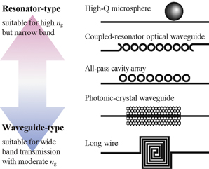
Figure 1. Schematics of various slow-light structures producing optical delays.
Download figure:
Standard image High-resolution imageFigure 2(a) shows the schematic of the photonic band in a standard photonic crystal waveguide without modifications, which was employed as phase shifters in the first generation MZ modulator. The photonic band is usually rounded and gradually flattened when the frequency approaches to the band-edge, corresponding to the Bragg condition of the periodic structure of the photonic crystal. With this flattening, ng increases. This is what we call band-edge slow light. When the refractive index of the photonic crystal slab is decreased and increased by the carrier injection and depletion, respectively, the band overall shifts upwards and downwards. In this situation, the shift of the wave number Δk is small in the fast light regime apart from the band edge, while it is enhanced in proportion to ng in the slow-light regime. The phase shift ΔΦ is given by ΔkL, thus slow light enhances the phase modulation. Figure 2(b) is a simple estimation of the phase shifter length required for a π phase shift, Lπ , when only one arm of the MZ interferometer is used as a phase shifter. When a rib waveguide with ng = 4 is used, Lπ becomes longer than 1 mm, as mentioned above. If photonic crystal waveguides with ng = 20 is used, Lπ can be shorter than 1 mm. If ng and/or the effective index change Δn becomes larger, one can expect Lπ to be ∼100 μm. Meanwhile, the push–pull drive is often used in MZ modulators. Here, both phase shifters are operated simultaneously in the opposite directions so that the total phase shift is eventually doubled. In this case, Lπ can be shortened to less than 100 μm. We may also be able to expect such slow-light enhancement to reduce the applied voltage and power consumption when Lπ is unchanged.
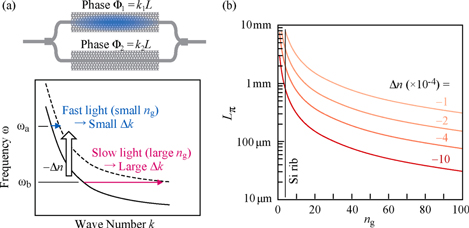
Figure 2. Slow-light enhancement in a photonic crystal waveguide. (a) Schematics of an MZ modulator based on the photonic crystal waveguide and band diagram. (b) Theoretical estimation of Lπ with ng, which is calculated from a simple formula for the phase shift Δϕ = k0 ng(Δn/n)L where k0 is the wave number in vacuum.
Download figure:
Standard image High-resolution image3. Fabrication technology
Photonic crystal waveguides can now be fabricated in wafer scale by using the open foundry services of the CMOS-compatible process [8], as shown in figure 3. To our knowledge, three major foundries are currently on service to worldwide general users, i.e., Interuniversity Microelectronics Centre (IMEC) [9], Laboratoire d'Électronique des Technologies de l'Information (LETI) [10], and Institute of Micro-Electronics (IME) [11]. There may be other foundries limited to users inside their countries or to those of research collaborators. They use 8 or 12 inch silicon-on-insulator (SOI) wafer as a substrate and a 180 nm generation process with stepper lithography and a KrF excimer laser (λ = 248 nm) or 130 nm generation process with ArF (λ = 193 nm). More advanced generation processes ≦̸ 90 nm using immersion ArF stepper are also tested in some research. An example size of the reticle (photomask sets) is 25 × 32 mm2, and so users can receive roughly 30 pieces of the same dies from the 8 inch wafer after dicing. The process recipe typically includes Si wire and rib waveguides, Si(O)N waveguides, passive components of these waveguides such as splitters, couplers and crossing, spotsize converters, grating couplers, heaters, p and n dopings, Ge epitaxial growth, contact holes, and metal vias, wires and pads. Device data are produced by users and submitted to foundries in GDS-II format, which is standardized for CMOS electronics. Due to very compact waveguides and devices of Si photonics, a huge number of devices can be placed in the reticle area. Each pattern on the photomask has to be corrected from the targeted pattern by considering the pattern size, exposure condition and proximity effect of the lithography, which are usually summarized as critical-dimension data. Therefore, the data production will be an unexpectedly heavy task in the situation that powerful computer-aided design (CAD) systems like those used in designing electronic circuits have not yet been developed in Si photonics. At this stage, each group produces data manually using general purpose CAD or using original software programs for producing corrected data automatically.
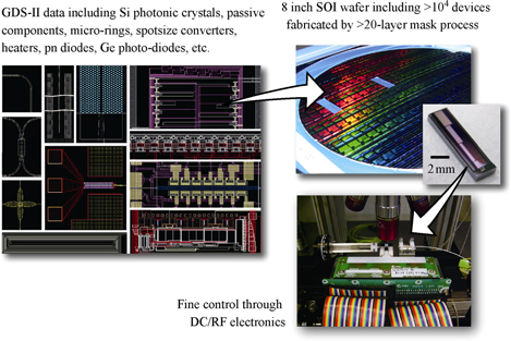
Figure 3. Fabrication of photonic crystal devices using Si photonics CMOS-compatible processes [3].
Download figure:
Standard image High-resolution imageIn many studies on photonic crystals reported so far, fragile air-bridge structures have been used to enhance the optical confinement into the slab. However, the formation of the air-bridge structure in wafer scale is still challenging although some foundries achieve it using specific processes of releasing the silica layer below the Si slab. Therefore, photonic crystal waveguides with silica claddings [12] are usually used for modulators. The thickness of the Si slab and the diameter and pitch of holes are typically 220, 200 and 400 nm, respectively. Such structures are fabricated similarly to other Si photonics components without particular difficulties. First, the Si layer is etched to form photonic crystal waveguides buttjoined to Si wire waveguides. Then, p+, p, n, n+ doping with typical concentrations of 2 × 10²⁰, 5 × 10¹⁷, 3 × 10¹⁷, 2 × 1020 cm−3, respectively, are performed to form the p–n diode structure. Then the whole structure is covered with silica. Finally, contact holes are opened and metal vias, wires and pads are formed.
4. Devices using band-edge slow light
Figure 4 shows our first generation device fabricated into 210-nm thick Si slab by using the 180 nm process [7, 13]. Both arms of the MZ interferometer have 200-μm-long phase shifters based on photonic-crystal waveguides to balance all the optical properties. However, the MZ interferometer is asymmetric; different length arms of 400-nm-wide Si wires are used so that the change of ng is visible in the transmission spectrum. For the splitter and combiner, a multi-mode interference type is used, whose theoretical loss is 0.3 dB at λ = 1.5–1.6 μm. I/O waveguides are terminated at ends of the die by spotsize converters, each of which consists of an inverse-tapered Si wire covered by a silica waveguide of 4 × 4 μm2 cross-section. Light is coupled from lensed fiber to the Si wire through the spotsize converter with a coupling loss of ∼2.5 dB, when the tip width of the inverse taper is 180 nm. If the tip width is reduced to 100 nm by employing higher-resolution lithography, the scattering loss is suppressed and the coupling loss will be reduced to less than 1 dB, which is acceptable for the practical use.
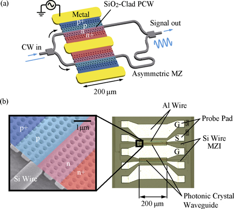
Figure 4. Si-photonic-crystal slow-light-waveguide MZ modulator (first generation). (a) Schematic. (b) Photograph of a fabricated device (right). The scanning electron microscopy image (left) was taken after removing the silica cladding. These figures are partly reproduced from [13].
Download figure:
Standard image High-resolution imageThe photonic band diagram of a standard photonic crystal waveguide and measured transmission and ng spectra of the MZ modulator are shown in figure 5. The light line in the band diagram indicates the critical condition between the optical confinement into and leakage from the slab covered by the silica claddings. In the air-bridge photonic crystal slab, the photonic band flattens abruptly near the band-edge. On the other hand, in the silica-cladded slab, the band flattens more gently. This reflects the gradual increase in ng in the measured spectrum; ng increases from 10 to 40. The transmission band is 15 nm wide. This width is determined by the light line and band-edge on the short and long wavelength sides, and cannot be changed so drastically unless the choice of materials is changed. The fringe in the transmission spectrum arises from the asymmetric MZ interferometer. The spacing between fringes decreases as ng increases. When ng becomes higher than 30, fast oscillation noise appears. It might be caused by the disordering in the fabricated device and enhanced backscattering, which is observed in the high ng regime [14]. This critical value of ng ∼ 30 is dominated by the process; ng > 30 values may also result in noise-free spectra, but with a more advanced process.
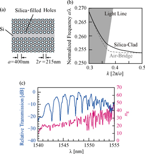
Figure 5. Photonic crystal waveguide. (a) Schematic structure. (b) Band diagram. (c) Transmission and ng spectra measured for MZ interferometer with photonic crystal waveguides [13].
Download figure:
Standard image High-resolution imageBefore showing RF performance, let us discuss passive losses in the MZ modulator. The loss from fiber to the Si wire waveguide is 2.5 dB/coupling. As mentioned above, it will be reduced to < 1 dB. The loss at the fabricated splitter and combiner is < 1 dB each, but theoretically 0.3 dB. The loss of the Si wire waveguide is 3 dB cm−1. Due to the excess wiring on a die in the sample, it results in a 1.5 dB loss. The junction loss between the Si wire and photonic crystal waveguide is ∼1.5 dB each, which have room for reduction. The propagation loss of the p–n doped photonic crystal waveguide is influenced by the free carrier absorption and also depends on ng and the quality of the sample. If the distance between the p+ and n+ regions is smaller than 4 μm, the absorption in these regions increases drastically. Even when the distance is set at the critical distance, the propagation loss is as large as 250 dB cm−1 for ng ∼ 20, which corresponds to 2.5 dB for L = 100 μm. The total loss is 8.5 dB on a chip and 13.5 dB from fiber to fiber. In the future, these values can be reduced to 6 dB and 8 dB, respectively, which are competitive with those in commercial LiNbO3 modulators.
In RF modulation measurements, continuous-wave laser light is coupled into to the Si wire waveguide through the spotsize converter. Sinusoidal electrical signals from synthesizer or non-return-to-zero (NRZ) pseudo-random-bit sequence (PRBS) electrical signals from pulse pattern generator (PPG) are amplified, mixed with dc bias through a bias-tee and applied to the device using an RF probe. The output light is coupled to another fiber and amplified by an erbium-doped fiber amplifier (EDFA). The signal undergoes optical-to-electrical (O/E) conversion, and its eye pattern is observed using a sampling oscilloscope. Figure 6(a) shows frequency responses of the modulator in both carrier injection and depletion modes, which are observed from the amplitude on the oscilloscope for the small amplitude sinusoidal signals. In the carrier injection mode, the 3-dB bandwidth is limited to 1 GHz due to the slow carrier diffusion time and lifetime. Therefore, the eye pattern for the NRZ PRBS signals does not open clearly even at 2 Gbps. On the other hand, in the carrier depletion mode, the 3-dB bandwidth is close to 10 GHz. In this measurement, the RF probe had a bandwidth of over 30 GHz, while the electrical amplifier, O/E converter, and RF module of the oscilloscope had a bandwidth of 18 GHz. Therefore, the observed bandwidth in figure 6 in the depletion mode might be affected by these RF components and the device bandwidth determined by the RC time constant might be higher than 10 GHz. In this device, the electrical resistance was measured to be 29 Ω, and the capacitance under small reverse bias voltages is calculated to be 50 fF, which corresponds to an RC time constant of 1.45 ps and a bandwidth of 110 GHz. To improve the device response in the carrier injection mode, pre-emphasized signals are used, in which the high-frequency components of the NRZ PRBS signals are particularly emphasized in advance. Such signals are produced by high-pass filtering or signal processing using a differential device. Figure 6(b) shows eye patterns of input 10 Gbps NRZ PRBS signals (left) and output signals (right) in both modes. In the carrier injection mode, strongly emphasized signals are used, and the eye pattern barely opens. The long-tailed fall time is 450 ps, which might be caused by the slow carrier diffusion. The rise time of 150 ps corresponds to the carrier lifetime and its wide jitter is caused by the pattern effect that different amounts of accumulated carriers of the PRBS signals show different responses. On the other hand, the eye pattern in the carrier depletion mode is opened more clearly due to the faster response, even though the pre-emphasis is modest. This was the first demonstrated with the 10 Gbps operation in Si MZ modulators with phase shifters as short as 200 μm length. Here, the RF voltage was 5.8 V in peak to peak, and the bit energy consumption was measured to be 2.6 pJ bit−1, which is the lowest level for MZ modulators; it is even lower than that reported for carrier injection type devices with similar length [15].
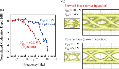
Figure 6. Performance of photonic crystal slow-light MZ modulator (first generation) [13]. (a) Frequency response for sinusoidal small signal. (b) Eye patterns of pre-emphasized drive signal (left) and output signal (right) at 10 Gbps.
Download figure:
Standard image High-resolution image5. Devices using LD slow light
Figure 7 shows the second generation device. Since the MZ interferometer is symmetric, its transmission spectrum does not show the fringes as observed in the asymmetric device. To observe and optimize the operating point of the interference, thermo-optic phase tuners are added in both arms. The total device footprint is mainly dominated by the arrangement of metal pads, and that of essential components is much smaller. In this device, modified photonic crystal waveguides, what we call the lattice-shifted photonic crystal waveguides (LSPCWs) [8, 16], are used to improve the spectral characteristics. Figures 8(a), (b) show the schematic and band diagram of the LSPCW. Here, the third row of holes from the line defect is shifted along the waveguide by an amount of s. Increasing s, the photonic band below the silica light line is partially pulled up due to the interaction of the waveguide band and slab mode bands of the photonic crystal, and exhibit a straight part giving a constant ng. Such a constant ng clearly appears in the ng spectra of figure 8(c). Increasing s, the monotonically increasing curve is deformed and the flat part appears finally within the transmission band. We call this flat part the low-dispersion (LD) band.
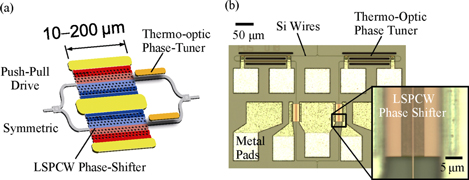
Figure 7. Si photonic crystal slow-light waveguide MZ modulator (second generation) [17]. (a) Schematic. (b) Photograph of fabricated device.
Download figure:
Standard image High-resolution image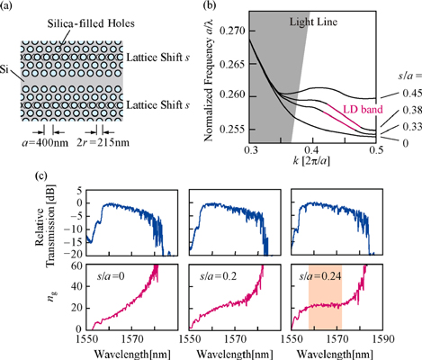
Figure 8. LSPCW. (a) Schematic structure. (b) Band diagram [8]. (c) Transmission and ng spectra for different shift s [18].
Download figure:
Standard image High-resolution imageFigure 9(a) explains how the operation as a phase shifter changes with the LSPCW. The same slow-light enhancement is maintained in the LD band. This is equivalent to the wide temperature tolerance. Since the photonic crystal slab exhibits the temperature dependence of 0.082 nm K−1 in the transmission spectrum, a certain wavelength in the 10-nm LD band maintains the modulator performance in the wavelength range of 120 K. Of course, the LD band can be shared for the wavelength and temperature tolerance. The balance between the constant ng and bandwidth ΔωLD of the LD band can be controlled to some extent from 15 to 30 by changing s. As already mentioned, it is constrained by the normalized delay-bandwidth product denoted by ng ΔωLD/ωLD = ng ΔλLD/λLD = Δn. Figure 9(b) summarizes the relation between these parameters. For the current design of shifting third rows of holes, Δn is calculated to be 0.15. If target ng are 15, 20, and 30, then ΔλLD at λLD = 1.55 μm become 14, 11 and 7 nm, respectively. Δn can further be enhanced and the balance is controlled more flexibly by shifting other rows of holes in the various directions. Some calculations indicate that Δn = 0.3 is obtainable by such optimizations.

Figure 9. Slow-light enhancement in LSPCW. (a) Schematics of photonic crystal waveguide MZ modulator and band diagram. (b) Theoretical relation between Δλ and ng simply calculated from the relation Δn = ng(Δλ/λ) at λ = 1.55 μm.
Download figure:
Standard image High-resolution imageThe second generation devices exhibit eye patterns for 10 Gbps NRZ PRBS signals, as shown in figure 10(a). Here, L of the LSPCW phase shifter is changed from 200 to 10 μm. ng distributes in the range of 15–20 in the samples. Since the RF electrical detector module of the oscilloscope in this measurement was exchanged to one with a bandwidth of 50 GHz, the eye opening quality for L = 200 μm is slightly improved. The open eye is confirmed up to L = 50 μm even though its amplitude is only 1 dB. Considering that most Si MZ modulators have L of several millimeters, this L is markedly short and clearly shows the slow-light enhancement. Figure 10(b) shows the bit-error-rate (BER) characteristics for the three longest devices in figure 10(a). The error-free operation is easily obtained for L = 200 μm. The BER reaches the 10−9 threshold but does not decrease further for L = 90 μm. It does not reach the threshold for L = 50 μm. Figure 10(c) shows the dependence of the BER characteristics on the bit length, where L = 200 μm and the bias is reduced to −3 V so that the BER characteristics are degraded. When the bit length is 27–1, BER becomes error-free easily. However, the error floor clearly rises inbetween 215–1 and 220–1, which correspond to 3.2 μs and 102 μs at 10 Gbps. Another measurement indicates that the thermal response time of a similar photonic crystal waveguide is 19 μs [19]. Therefore, the error floor might be caused by long-range thermal fluctuations.
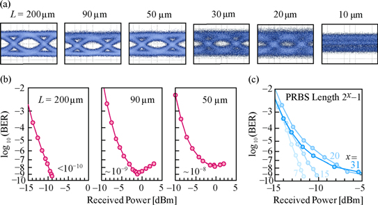
Figure 10. Modulation characteristics measured at 10 Gbps from a slow-light MZ modulator (second generation) based on a Si photonic crystal. (a) Eye patterns for various L. (b) BER characteristics [18]. (c) Dependence of BER on PRBS bit length.
Download figure:
Standard image High-resolution imageFigure 11 summarizes performance measured with the bias voltage VDC for L = 200 μm. Here, Vpp is determined so that the eye pattern opens most widely, and other parameters are measured on this condition. The best Vpp ranges from 3 to 4 V when VDC is less than −4 V. In this regime, the excess loss at the RF modulation is ∼1 dB and the extinction ratio (ER) is as large as 10 dB. The RF power consumption is estimated to be ∼2 pJ bit−1 due to the reduced voltage and push-pull drive. When VDC is −3 V or higher, Vpp should be reduced to 2 V. Even on this condition, a large ER of 9 dB is maintained. For such a low voltage, the error-free operation was not obtained. Still we expect to obtain it error free by optimizing the measurement condition particularly at the EDFA and O/E converter, which might add some excess noise.
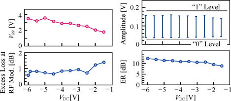
Figure 11. Modulation characteristics measured at 10 Gbps from a 200-μm-long slow-light MZ modulator (second generation) based on a Si photonic crystal. The details of the device and measurement setup are the same as those in [18] except the device length.
Download figure:
Standard image High-resolution imageAs mentioned above, LD slow light in the LSPCW is expected to have large wavelength and temperature tolerance in the modulator. Figure 12 demonstrates these expectations. Since L = 90 μm and ng ∼ 14, the eye amplitude is narrower than that for L = 200 μm in figure 13. If the effective ΔλLD for the modulator is assumed to be the range that maintains the eye amplitude within ±20% variations, ΔλLD is estimated to be as wide as 16.9 nm. Actually almost the same eye pattern is maintained in this range when the operating and measurement conditions are not changed at all but only the wavelength. Similarly, the eye amplitude is almost maintained when the device temperature is varied from 19 to 124 °C. The eye pattern is also unchanged in this temperature range. These are promising results toward the applications in optical interconnects.
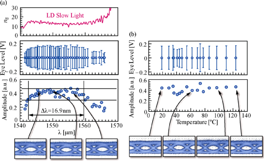
Figure 12. Wavelength (a) and temperature (b) tolerance at 10 Gbps modulation [18].
Download figure:
Standard image High-resolution image
Figure 13. Single-type slow-light MZ modulator based on Si photonic crystal [17]. (a) Schematic structure. VOA stands for variable optical attenuator. (b) Transmission spectrum. The color plot is taken by changing the heating power of the thermo-optic phase tuner.
Download figure:
Standard image High-resolution image6. High-speed operation
Considering the principle of the carrier depletion mode, the modulator has the potential to operate at higher speeds beyond 10 Gbps. Currently, however, our measurement setup lacks sufficient tools and components for speeds beyond 10 Gbps. Because of this, a device, as shown in figure 13(a), was designed, where only one arm has the LSPCW phase shifter and the other reference arm consists of a long wire waveguide delay line [17]. Its length is designed so that optical delays in two arms are the same when ng in the LSPCW equals 30. Since the LSPCW is more lossy than the wire waveguide, a thermo-optic MZ variable attenuator is also inserted into the reference arm. Such a modulator only needs one electrical amplifier to operate. Moreover, we can avoid the spectral noise at ng > 30. As mentioned, the noise occurs due to the enhanced backscattering in the presence of disordering. It is also caused by a small phase mismatch between two arms, which is also enhanced by the slow-light effect. The latter problem is avoided by using slow light only in one arm. Figure 13(b) shows the transmission spectrum changed by the heating power of the thermo-optic phase tuner. In the color plot, sloped lines at shorter wavelengths of the LD band show that the optical delays are not the same. The curves are then flattened at longer wavelengths, suggesting that the same delay is obtained and the corresponding ng is 30. Figure 14 shows eye patterns at 25 and 40 Gbps, exhibiting barely open eye under the condition ng = 30. Since such open eye is not observed at shorter wavelengths with lower ng, it is attributed to the high ng of slow light. These results are obtained with PPGs and an electrical amplifier, which are different from those at 10 Gbps, with narrower tuning flexibility. If high-quality and high-speed equipment is used, clearer eyes as well as detailed modulation characteristics will be clarified.
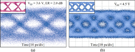
Figure 14. Eye patterns of single-type slow-light MZ modulator based on Si photonic crystal [18]. (a) 25 Gbps. (b) 40 Gbps. Insets are those of electrical signals from PPG. For (a), a different sampling oscilloscope was used. Since its integration speed is lower, the pattern looks slightly noisy.
Download figure:
Standard image High-resolution image7. Conclusion
We demonstrated Si MZ modulators with phase shifters based on photonic crystal waveguides, in which the modulation efficiency is enhanced in proportion to the group-velocity refractive index ng of slow light. The clear open eye and error-free operation are confirmed at 10 Gbps in the carrier depletion mode for phase shifter lengths of 200 μm and even less than 100 μm. The dispersion-engineered slow light enables stable operation in the wavelength range of 16.9 nm and the temperature range from 19 to 124 °C. The depletion mode has a potential of higher-speed operation. Actually, we observed an open eye at 25 and 40 Gbps even with primitive measurement equipments.
Figure 15 summarizes the relation between operating voltage Vpp and L in Si MZ modulators reported in the literature [18]. Most results of conventional devices are distributing on the right thick blue line. With the slow-light enhancement, this line is shifted to the left side, suggesting roughly 10-fold improvement. ng itself is five times larger than the value in Si rib waveguides in conventional modulators. Therefore, this improvement is not only attributed to the slow-light enhancement but also due to some improvement in electrical properties of the very short modulator, for which the phase matching between light waves and electrical signals. The bit energy consumption of our 200 μm modulators was as low as 2–3 pJ bit−1 even though Vpp was as high as 4–5.8 V. If the voltage is lowered to less than 2 V, the bit energy consumption will reach a fJ/bit regime, which will be an important advancement for optical interconnects.

Figure 15. Operating voltage versus phase shifter length characteristics in Si MZ modulators reported so far. This figure was reproduced from [17].
Download figure:
Standard image High-resolution image
Presented results in this article are preliminary, and further investigations and optimizations are necessary for practical use. Still we believe that this modulator will be accepted and used widely in the near future because the slow-light effect certainly upgrades Si modulators by a factor of 5–10 and its fabrication using CMOS-compatible processes is almost the same as those for other Si photonics components. The main issue to be solved is the reduction of loss mainly in photonic crystal waveguides and at the junctions with I/O waveguides. Current on-chip loss of 8.5 dB should be reduced to 6 dB or more to meet the required power budget of optical interconnects.
Acknowledgements
This work was partly supported by the FIRST Program of JSPS and Future Development Project of METI/NEDO.