


Abstract
By way of a brief review of Si photonics technology, we show that significant improvements in device performance are necessary for practical telecommunications applications. In order to improve device performance in Si photonics, we have developed a Si-Ge-silica monolithic integration platform, on which compact Si-Ge–based modulators/detectors and silica-based high-performance wavelength filters are monolithically integrated. The platform features low-temperature silica film deposition, which cannot damage Si-Ge–based active devices. Using this platform, we have developed various integrated photonic devices for broadband telecommunications applications.
Export citation and abstract BibTeX RIS

Content from this work may be used under the terms of the Creative Commons Attribution-NonCommercial-ShareAlike 3.0 licence. Any further distribution of this work must maintain attribution to the author(s) and the title of the work, journal citation and DOI.
1. Introduction
Telecommunications network systems are now facing an explosive traffic increase with a growth rate of 30% per year [1]. Within 10 years, energy consumption and capital/operating expenditures in network systems will increase by 10 times or more; however, from economic and environmental viewpoints, such large and rapid growth is not sustainable. One of the breakthrough technologies for dealing with this information explosion is high-density photonic integration with ultra-small photonic devices. The smaller the device, the less power required. Moreover, integrated photonic functions with redundancy enable flexible and energy-efficient network operation [2]. Si photonics, one of the most promising technologies for such high-density photonic integration, enables monolithic integration of photonic devices made of Si and Ge on a Si wafer. Si photonics has the following superior features as an integrated photonic technology. Optically, Si is transparent and shows a large refractive index in the 1200−1700 nm telecommunications wavelength band. Therefore, it can be used to construct very compact photonic devices. Electrically, Si is a semiconductor. Therefore, carrier control in Si provides various active functions, such as optical modulation. Moreover, electronic logic would provide intelligence and flexibility in photonics. Physically, Si devices and substrate are robust and tough enough for various types of heterogeneous integration, which provides further functionalities. Of course, the Si platform is very reliable and has superior capabilities for cost-effective mass production. Among these features, the compactness of Si photonics has had the largest impact. Figure 1 compares cross sections and bending for a Si photonic wire waveguide and conventional silica waveguide. As shown in this figure, the Si photonic wire waveguide has an extremely small core and bending radius. The origin of the compactness is a strong internal reflection at the Si–silica interface, or very strong light confinement. Using this waveguide, we can significantly reduce the size of photonic devices and integrate them with high density [3]. Figure 2 shows the potential of Si photonics technology in data transmission systems. Thanks to the compactness of Si photonics devices, increases in both energy efficiency and integration density of about 100 times over those of conventional technology can potentially be achieved. Although such improvement is expected in a wide range of applications, from on-chip interconnects to long-distance telecommunications, the hurdles for telecommunications applications are still very high. In telecommunications applications, where long-distance optical transmission is essential, devices should have low optical losses, low interchannel crosstalk, and insensitivity to polarization.

Figure 1. Core size and bending radius of conventional silica waveguide and silicon photonic wire waveguide.
Download figure:
Standard image High-resolution image
Figure 2. Potential of silicon photonics in data transmission applications.
Download figure:
Standard image High-resolution imageIn this article, we briefly review the Si photonics technology and introduce a Si-Ge-silica photonic integration platform as one of the improved Si photonics technologies specialized for high-performance telecommunications applications.
2. Brief review of Si photonics technology
Si photonics technology is categorized into six sub-technologies: waveguide systems, passive devices (such as wavelength filters), modulators, detectors, light sources, and integration. For waveguide systems, the propagation loss of Si wire waveguides reaches around 1 dB per centimeter, which is low enough for the photonic integration on a Si chip with an area of a few square centimeters. Such a low-loss waveguide was fabricated by using state-of-art processing technology that offers a line edge roughness of less than 1 nm [4]. The loss of coupling to an external fiber has also been reduced to less than 1 dB by using a spot-size converter with an inverse taper [5]. We can also use a surface grating coupler, which allows wafer-level photonic inspection [6].
Using this low-loss waveguide system, various passive devices—such as lattice filters [7], cascaded ring resonator filters [8], and arrayed waveguide gratings filters (AWGs) [9, 10] for wavelength division multiplexing (WDM) systems—have been developed. The crosstalk to neighboring channels is typically 15–20 dB, which seems low enough for practical interconnects; however, this level of crosstalk is a major issue for telecommunications applications. Moreover, these passive devices have serious polarization dependence, which should be thoroughly eliminated for practical applications by using a special polarization diversity technology [11].
The next devices discussed are optical modulators. Presently, there are three types of Si-based optical modulators: the Mach–Zehndar interferometer (MZI), ring resonator, and electro-absorption (EA) modulator. In the MZI, the refractive index of the optical waveguide of one interferometer arm is modulated electrically, and the interference condition is changed. In the ring resonator, the refractive index of the ring is modulated, and the resonance wavelength is changed. The EA modulators using Franz–Keldysh or QCSE effects have also been proposed [12]. However, they can work only as intensity modulators for a limited wavelength band. Because of this, Si-based MZIs and rings are presently being intensively developed. The refractive index can be changed by controlling the carrier density in the waveguide core. The carrier control structures are categorized as p–n depletion type, metal-oxide-semiconductor (MOS) type, and p–i–n injection type. Table 1 summarizes the performance of the modulators. As shown, the modulation speed of these devices has already exceeded 10 Gbit s−1, while other aspects of performance vary with the modulation type. For example, a p–n MZI shows good performance in extinction ratio and linearity, while other types show much better performance in device size and power efficiency. In other words, device selection depends on the intended applications. For example, a p–n MZI is suitable for telecommunications [13, 14], for which high-performance modulation is needed. On the other hand p–i–n MZIs and ring modulators are suitable for on-chip interconnects [15–17], in which small size and low power consumption are the most important issues.
Table 1. Performance summary of Si optical modulators.
| p–n MZI | MOS MZI | p–i–n MZI | Ring/EA | |
|---|---|---|---|---|
| Operation speed | 10–40 Gbps | ~30 Gbps | 10–50 Gbps | >10 Gbps |
| Extinction ratio | ~10 dB | <10 dB | ~5 dB | 5–7 dB |
| Linearity/chirp | Good | Good | Moderate | Poor |
| Device length | 3–5 mm | ~1 mm | <500 μm | <100 μm |
| Energy efficiency | >10pj/bit | ~1 pJ/bit | ~1 pJ/bit | 0.01–0.1 pJ/bit |
The next devices discussed are photodetectors (PDs). At present, detectors are categorized into two types: Ge on Si and indium phosphide (InP) on Si. The Ge PD is the most popular detector in Si photonics. It can be constructed on Si substrate monolithically [18], and its performance is comparable to that of conventional InGaAsP devices, except for the dark current [19]. Dark current determines the lowest detection limit of optical power, and the present level of dark current for Ge PDs is acceptable for interconnects, but it represents a critical issue for telecommunications applications. InP-based devices constructed by using various hybrid integration technologies guarantee performance [20, 21], but complicated integration of fragile InP-based devices on a Si wafer would raise fabrication costs.
Light sources are the most critical components in Si photonics because Si cannot emit light for the telecommunications wavelength band. Therefore, InP-based devices are the only solutions at present. There are three configurations of InP-based light sources on Si: off-chip, on-chip, and on-Si- substrate. The off-chip configuration guarantees performance but requires a large area. The on-chip configuration also guarantees performance [22]; however, precise chip alignment and cooling are issues. With a sophisticated wafer-bonding technique, the on-Si-substrate approach, or evanescent coupling of InP-based devices, guarantees compactness and the capability of large-scale integration [23]. However, reproducibility and cooling are issues. Since, as mentioned above, device performance shows trade-offs with integration density, device selection would depend on the intended applications. Although electrically pumped laser diodes have been developed by using heavily doped Ge-on-Si [24], intensive improvements in efficiency and cooling are needed for practical applications.
Although there are some performance insufficiencies, we can now get a device set on a Si wafer. That brings us to the next issue, which is their integration. For example, AWG wavelength filters and high-speed Ge PDs have been recently integrated for WDM data transmission systems [25]. Since typical Ge PD works at a data rate of over 10 Gbit s−1, total receiver bandwidth reaches a few hundred Gbit s−1 or more. However, we must bear in mind that Si-based AWGs are not applicable to telecommunications applications, as shown in the next section. High-density photonic integration for on-chip interconnection has also been developed intensively. Si modulators and Ge detectors are monolithically integrated on a SOI wafer, and multi-channel LD chips are mounted by a unique flip-chip bonding method [26]. The transmission bandwidth density of the device reaches 30 Tbit s−1 cm−2, which would satisfy the bandwidth requirement of chip-to-chip interconnects in 2020.
Monolithic photonic-electronic integration has also been achieved by using the standard complementary MOS (CMOS) foundry [27] and has already been implemented in commercially available active optical cables. Using a hybrid integration technology based on the evanescent coupling system mentioned above, a compact and cost-effective optical link module has also been developed [28].
3. Si-Ge-silica monolithic photonic integration platform for telecommunications applications
The photonic devices on the Si-Ge photonics platform covered in the previous section seem to be ready for practical use in short–reach computer interconnect applications. One of the key challenges for computer interconnects is ultra-high-data-rate connectivity within a small footprint, which would be achievable with Si photonics technology. However, Si photonics technology in its present form is not applicable to telecommunications, as telecommunications systems require low-loss photonic devices to extend the communication distance and the number of branches. Furthermore, long-distance communication poses several additional problems regarding polarization, which are not a concern in short-reach computer interconnects.
For example, in dense WDM transmission systems, inter-channel crosstalk should be about −25 dB or less. The present Si photonic platform, however, cannot provide such high-performance photonic devices. Several wavelength filters based on Si photonic wire waveguides have been reported [9, 10], but none of them meet the requirements for telecommunications applications. Since the effective refractive index of a Si photonic wire waveguide is extremely sensitive to the core geometry, the geometrical tolerance required is far below the errors in present fabrication technology. For example, a 1 nm geometrical error significantly increases the inter-channel crosstalk of a wavelength filter to −18 dB, which is not acceptable for telecommunications applications [29]. For the same reason, it is virtually impossible to eliminate polarization dependence in Si-based WDM systems.
In order to eliminate these obstacles to practical telecommunications applications, some assisting technologies should be implemented in Si photonics. Here, we will call such technologies intelligence assists and material assists, as shown in the long-distance part of figure 1. Intelligence assists are performance compensation techniques based on digital electronics, which are now being developed for digital coherent transmission systems. Material assists are techniques for improving performance by introducing the right materials for the right functions. One of the most promising material-assist technologies is Si-Ge-silica photonic integration, which could relax the geometrical tolerance in high-performance passive devices.
Recently, we have developed such a Si-Ge-silica photonic integration technology, by which high-performance silica-based passive devices and Si-Ge-based compact active/dynamic devices can be monolithically integrated [30]. In the following sections, we report the details of the Si-Ge-silica monolithic integration platform: an improved Si photonics for high-performance telecommunications applications.
3.1. Waveguide system
Figure 3 shows a schematic image of the Si-Ge-silica monolithic integration platform. This platform consists of Si waveguide–based dynamic/active devices (such as Si modulators and Ge detectors), silica waveguide–based high-performance passive devices (such as wavelength filters), and inverse-taper spot-size converters (SSCs), which connect the Si and silica waveguides to each other [31]. These devices are monolithically fabricated on a Si-on-insulator (SOI) wafer. Si- and Ge-based devices can be integrated by using conventional Si photonics technology. However, additional silica-based devices cannot be integrated by using conventional technology, because conventional silica waveguide fabrication generally involves processes with temperatures exceeding 1000 °C for silica film deposition [32]. Such a high-temperature processes can destroy the Si-Ge electronic structures for modulators and detectors. Our monolithic integration process features low-temperature silica film deposition using the electron-cyclotron-resonance plasma-enhanced chemical vapor deposition method (ECR-PECVD) [33]. In ECR-PECVD, silica-based materials such as silicon oxynitride (SiOx Ny ) and silicon-rich silica (SiOx ) are deposited. For the SiOx Ny , a gas mixture of O2, N2 and SiH4 is used, and for the SiOx deposition, O2 and SiH4. The O2 and N2 gases are introduced into the plasma chamber, and the SiH4 gas is introduced into the deposition chamber. ECR plasma generated in the plasma chamber is transported to the deposition chamber by a divergent magnetic field and irradiated to a wafer in the deposition chamber. The energy of the ions irradiated to a wafer is about 10–20 eV [34]. This moderate energy induces a reaction on the wafer surface so that high-quality films are formed at low temperatures. As the ECR-PECVD system does not add bias to the substrate, the wafer temperature during the film deposition can be kept below 200 °C even without wafer cooling. To control the refractive index of the deposited films, the flow rate of O2 and N2 for SiOx Ny films and the flow rate of O2 for SiOx films are adjusted, with the flow of SiH4 maintained at a fixed rate. Figure 4 shows the refractive index and deposition rate as a function of gas flow rate. Index controllable ranges are 1.47–1.72 for SiOx and 1.47–1.95 for SiOx Ny . The deposition rate is over 100 nm min−1. Table 2 shows the atomic percentages of the core and clad films of SiOx and SiOx Ny waveguides with a refractive index difference Δ of ∼2.9%.

Figure 3. Schematic of Si-Ge-silica monolithic integration platform for Ge PD.
Download figure:
Standard image High-resolution image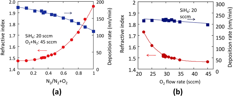
Figure 4. Refractive index and deposition rate as a function of gas flow rate: (a) SiOxNy and (b) SiOx.
Download figure:
Standard image High-resolution imageTable 2. Atomic percentages of core and clad films.
| Sample name | Refractive index | Si(%) | O(%) | N(%) | Others(%) |
|---|---|---|---|---|---|
| SiOx core | 1.52 | 34.1 | 57.6 | — | 8.3 |
| SiOx Ny core | 1.51 | 32.0 | 59.0 | 4.9 | 4.1 |
| Clad | 1.47 | 30.7 | 62.6 | — | 6.7 |
| Thermal oxide | 1.46 | 33.8 | 66.2 | — | — |
The atomic percentages were measured by Rutherford backscattering spectrometry, and we confirmed that the composition of the thermal-oxide film (reference) was precisely measured to be SiO2.0 by this technique. The compositions of the SiOx core, the SiOx Ny core, and the clad films are SiO1.7, SiO1.8N0.2, and SiO2.0, respectively. These results show that the refractive indices of the silica-based films can be successfully controlled by the atomic ratio of Si/O (N). Here, for the WDM devices, the SiOx core is used for most of the passive devices because it has lower optical absorption in the C-band than the SiOx Ny core.
Figure 5 shows transmission characteristics of monolithically integrated Si and SiOx waveguides with a Δ of 2.9%. The core sizes of the Si and SiOx waveguides are 200 nm × 400 nm and 3 μm × 3 μm, respectively. In the sample preparation, before constructing the SiOx waveguides, the Si waveguide core was fabricated using electron beam lithography and low-pressure-plasma reactive ion etching. The propagation losses of the Si and SiOx waveguides on the Si-Ge-silica monolithic platform are less than 3 dB cm−1 and 0.9 dB cm−1, respectively. Without Ge, these losses can be further reduced to 1 dB cm−1 and 0.6 dB cm−1, respectively [33]. The increase of propagation losses might be due to the imperfection of the SiO2 mask for Ge selective growth. The polarization-dependent propagation loss of the SiOx waveguides is less than 0.1 dB cm−1 [35].
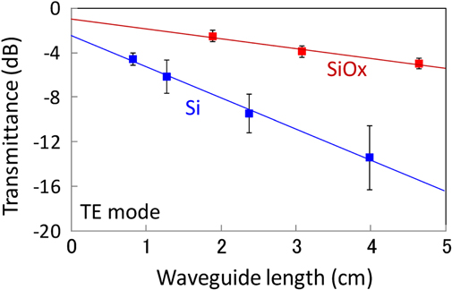
Figure 5. Transmission characteristics of Si and SiOx waveguides. Reproduced with permission of [38]. Copyright 2013 IEEE.
Download figure:
Standard image High-resolution imageFigure 6(b) shows the relationships between transmittance and the number of SSCs between Si and SiOx waveguides. In the measurement sample, several SSCs are connected between Si and SiOx waveguides, as shown in figure 6(a). The size of the taper tip of the SSCs is 200 nm × 80 nm, which provides a reflection ratio at the taper region of less than −40 dB [36]. The measurement results show that the coupling loss per SSC is 0.35 dB for a TE-like mode light, in which the dominant electric field is parallel to the substrate. We also measured the coupling loss with a TM-like mode light, in which the dominant electric field was normal to the substrate. The coupling loss per SSC is 0.31 dB. Thus, the inverse taper SSCs show polarization insensitivity. The conversion loss is, of course, low enough to meet the severe telecommunications-grade requirements on the platform.

Figure 6. (a) Schematic of sample for SSC-loss measurement. (b) Measured transmittance as a function of the number of SSCs. Reproduced with permission of [38]. Copyright 2013 IEEE.
Download figure:
Standard image High-resolution imageFigure 7 shows the transmission spectra of a Si photonic wire waveguide with SSCs. Although there is absorption due to O-H residue in the SiOx film, the applicable bandwidth of the SSC is very wide, ranging from 1400 to 1700 nm for 1-dB loss.

Figure 7. Transmission spectrum of Si photonic wire waveguide with SSCs.
Download figure:
Standard image High-resolution image3.2. Stand-alone devices
Using SiOx waveguides, we have developed a 12-channel AWG filter with 1.6 nm channel separation. Figure 8 shows the structure and filtering spectra of the device. Fiber-to-fiber insertion loss is 5 dB, and inter-channel crosstalk is less than −25 dB. Thanks to a large waveguide core and moderate index contrast, the filtering performance is better than that in Si-based AWGs. The insertion loss and crosstalk would be further improved by applying sophisticated designs developed for conventional silica waveguide devices. Although small polarization dependence due to film stress remains in the AWG, we can compensate for this by introducing a multilayer core technology using SiOx and silicon nitride films [35].

Figure 8. Structure (a) and filtering spectra (b) of the SiOx AWG.
Download figure:
Standard image High-resolution imageOn this Si-Ge-silica photonic platform, we have also developed some modulation and detection devices. Figure 9 shows the structure and attenuation performance of a Si-based variable optical attenuator (VOA). The VOA is a kind of modulation device implemented with a simple lateral p–i–n diode in a rib-type Si waveguide. In the fabrication, the Si layer including the p–i–n diode structure and electrodes was constructed by the conventional CMOS electronics process. Then, SiOx waveguides for the SSCs were formed. Carriers injected in the waveguide core absorb light, and thus optical power can be modulated precisely. The dynamic range of the device is over 20 dB, and the frequency response is about 100 MHz. Since it is not an interference device, we can eliminate polarization dependence by applying a careful design of the core shape. As shown in figure 9(b), the polarization-dependent loss (PDL) is reduced to about 1 dB, which includes losses in the device and fiber coupling [37]. This VOA is advantageous in dynamic range and polarization dependence, but its response is not very fast. For fast optical modulation, we have already developed a depletion-type device and have observed modulation at over 10 Gbps.

Figure 9. Structure (a) and attenuation performance (b) of the VOA.
Download figure:
Standard image High-resolution imageFigure 10(a) shows the structure of a Ge-based photodiode (Ge PD) with a Si waveguide input [38]. The fabrication process for a Ge PD on the Si-Ge-silica platform is much more complicated than that of modulation devices. First, Si waveguide cores and tapers for SSCs are fabricated on the SOI wafer, and boron implantation for p-type electrodes is performed. Next, selective growth of Ge is performed by using the ultra-high-vacuum CVD method [39], and a thin Si film is deposited on the Ge surface to prevent the Ge film from being damaged during subsequent processes. After that, phosphine is implanted into the top of the Ge PD, followed by the formation of Ti/TiN/Al electrodes. Then, SiOx film is deposited by using ECR- PECVD, which is then etched to form cores of SiOx waveguides. Finally, an over-cladding SiO2 film is deposited and contact holes are formed. Figure 10(b) shows current–voltage curves of a Ge PD in the dark and in the illuminated state. Input light power was 0.36 mW at the SSC before the Ge PD. Dark current and photocurrent are 56 nA and 0.4 mA at a −1 V bias. The responsivity of the stand-alone Ge PD is estimated to be about 1.1 A W−1 at the entrance of the SSC. The series resistance of the Ge PD is estimated to be ∼140 Ω by a linear fitting. The low parasitic resistance makes it possible to reduce RC delay and improves the operation speed of the PD. The frequency response of the Ge PD is shown in figure 10(c). The 3 dB cutoff frequency is about 20 GHz at a −1 V bias, which would be fast enough for application to 25 Gbps data transmission. The relationship between photocurrent and wavelength is shown in figure 11 [38]. Ge PDs show flat wavelength dependence in the C-band, and the polarization dependence of the power amplitude is less than 1.0 dB.

Figure 10. (a) Structure, (b) I-V characteristics, and (c) frequency response of Ge PD.
Download figure:
Standard image High-resolution image
Figure 11. Wavelength dependence of the photocurrent of Ge PD with TE and TM mode input. Reproduced with permission of [38]. Copyright 2013 IEEE.
Download figure:
Standard image High-resolution image4. Photonic integration for WDM systems
4.1. AWG-VOA integration
Using ECR-PECVD, we can integrate silica-based high-performance passive devices with Si-based active devices. As an example, we have demonstrated an integrated AWG-VOA [40], which is an important component as a variable-attenuator multiplexer/demultiplexer (VMUXs/DEMUXs) in photonic networks. Figure 12(a) shows the structure of a fabricated VOA-AWG integrated device. The Si VOA is basically the same as the one mentioned in the previous section. The AWG, which is for wavelength demultiplexing in 16 channels with 1.6 nm spacing, was made with Δ2.9% SiOx waveguides. Since the device layout has a large margin, the footprint of the device chip, at 15 × 8 mm2, is somewhat large. By optimizing the device layout, the chip size can be reduced to less than 10 × 10 mm2. Owing to the Si-VOA and SiOx -AWG, this device exhibits wavelength demultiplexing and high-speed intensity adjustment in each channel. Figure 12(b) shows the intensity adjustment results for every channel of the integrated VOA-AWG device. Arbitral power adjustment over a 15 dB dynamic range is achieved, and inter-channel crosstalk is less than −23 dB for zero attenuation. The response time of the VOAs is as fast as 15 ns. The polarization dependence of this AWG-VOA device can be eliminated by applying a multilayer core structure in the AWG and carefully designing the waveguide core in the VOA [35]. Figure 13 shows a close-up of the attenuation spectra of a channel of the device with polarization treatment. Throughout the attenuation range over 20 dB, the polarization-dependent wavelength shift (PDλ) and PDL are supressed to less than 0.1 nm and 2 dB, respectively. The complete function of these VOAs means that the integration of a silica-based device does not degrade the performance of Si-based active devices.

Figure 12. Structure of the AWG-VOA (a) and demonstration of multi-channel intensity adjustment (b). Reproduced with permission of [30]. Copyright 2013 IEEE.
Download figure:
Standard image High-resolution image
Figure 13. Attenuation performance of the AWG-VOA for different polarizations: (a) transmission spectra; (b) PDL and PDλ. Reproduced with permission of [30]. Copyright 2013 IEEE.
Download figure:
Standard image High-resolution image4.2. AWG-PD integration
We have also integrated Ge PDs and an AWG. Figure 14 shows a structure of the device [38]. The AWG is basically the same as that in the AWG-VOA integration, except for the polarization treatment. In this device, we use a single-layer SiOx core for a feasibility check of the integration process, so the AWG has a PDλ of ∼2.0 nm. The Ge-PD is the same as that described in the previous section. At the each output of the AWG, Ge PDs are connected via SSCs. Measured demultiplexing (DEMUX) spectra for all 16 channels of the Ge PDs are shown in figure 15(a) [38]. The spectra show a channel spacing of 1.6 nm as designed, and inter-channel crosstalk is around −22 dB or less. The insertion loss of the AWG at the central wavelength is about 5.1 dB, which includes waveguide propagation loss of 1.8 dB and diffraction loss of 3.3 dB. The fiber-to-waveguide coupling loss is 0.48 dB facet−1. The fiber-to-PD responsivity, which is normalized at the input power before the AWG, is 0.29 A W−1 at the central wavelength. The monolithic integration of the high-performance SiOx AWG with Ge PDs contributes to lowering crosstalk and increasing responsivity compared to a Si AWG with Ge PDs [41] and a SiN AWG with Ge PDs [42].

Figure 14. Structure of the AWG-PD.
Download figure:
Standard image High-resolution imageNext, we input non-return to zero (NRZ) pseudo-random bit sequence (PRBS) data with pattern length of 231−1 into the AWG. Measured eye diagrams of DEMUX photocurrent with 22 Gbps signal inputs for all channels are shown in figure 15(b) [38]. We confirmed that all 16 channels show clear opening eyes. The AWG-PD chip achieves total system bandwidth of 352 Gbps. Here, the bit rate was limited to 22 Gbps by the measurement equipment. Since the Ge PDs can work at 25 Gbps as mentioned in the previous section, the total system bandwidth could potentially reach 400 Gbps.
To confirm the feasibility of the device for practical network applications, we examined long-distance transmission. Continuous-wave infrared light from a tunable laser diode was modulated by a lithium-niobate Mach–Zehnder modulator. The modulation format is simple intensity modulation with 12.5 Gb s−1 NRZ PRBS data. The word length was 231−1. The signal bandwidth was restricted to 12.5 Gb s−1 by our experimental equipment. The modulated optical signal was transmitted through standard single-mode fibers (SSMFs) with dispersion of 17 ps km−1 nm−1 at distances of 20, 40, and 60 km. Then, to emulate a real receiver, we used a commercial clock-data recovery (CDR) module. The input signal was tapped by a 10 dB coupler and guided into the CDR module. After polarization preparation, the signal was input into the AWG-PD device by butt coupling of a high-NA fiber. The experiment was performed at room temperature without temperature control. The electrical signals from the Ge PDs were detected by an oscilloscope. The signal was also put into an error detector for bit-error rate (BER) measurement without transimpedance amplifiers (TIAs). The recovered clock was distributed from the CDR module to the OSC and ED.
Figure 16 shows measured BER curves obtained from channel 12 for various transmission distances and a received eye diagram after 40 km transmission (inset) [38]. The channel numbers are shown in figure 15(a). We confirmed error-free signal transmission up to 40 km. The receiver sensitivity measured at the AWG input was –6.8 dBm for the BER of 10–9 after 40 km transmission. After 60 km transmission, the BER was increased considerably by waveform distortion due to the dispersion and nonlinearity of the fiber. Taking into account the transmission loss of the AWG, we estimated the sensitivity of the Ge PD on channel 12 to be −13.6 dBm for the 40 km transmission. Although the theoretical sensitivity of the AWG-PD device is −32 dBm, estimated from shot noise and Johnson noise [43], the measured sensitivity was restricted by the measurement system, in that there were no TIAs on this chip. We believe the sensitivity will be improved by on-chip integration of TIAs, which, as we reported previously, has been already carried out [44].

Figure 15. DEMUX spectra of the AWG-PD chip (a) and eye diagrams of DEMUX photocurrent with 22-Gbps signal for all channels (b). Reproduced with permission of [30, 38]. Copyright 2013 IEEE.
Download figure:
Standard image High-resolution image
Figure 16. BER curves of channel 12 for various transmission distances and eye diagram after 40 km transmission (inset). Reproduced with permission of [38]. Copyright 2013 IEEE.
Download figure:
Standard image High-resolution image
5. Summary
Through a brief review of Si photonics technology for energy-efficient and cost-effective information trading applications, we have revealed that significant improvements in device performances are necessary for practical telecommunications applications. In order to improve device performance, we have developed a Si-Ge-silica monolithic integration platform, on which Si-Ge–based compact modulators/detectors and silica-based high-performance wavelength filters are monolithically integrated. The platform features low-temperature silica film deposition, which cannot damage Si-Ge–based active devices. Using this platform, various integrated photonic devices have been developed for broadband telecommunications applications. In an integrated AWG-VOA device, multichannel optical power adjustment with large dynamic range and low polarization dependence has been achieved. An integrated AWG-PD device works very well as a 400 Gbit s−1 WDM receiver.
Since the right materials are applied for the right functions, the Si-Ge-silica platform can provide well-balanced performance for telecommunications applications, whose specifications are too severe for the conventional Si-based photonic platform. In the next stage, we have to find ways to integrate electronic devices on the Si-Ge-silica photonics platform because a practical network system consists of both electronics and photonics.