


Abstract
A powerful model to evaluate the collective magnetic response of large arrays of segmented nanowires comprising two magnetic segments of dissimilar coercivity separated by a non-magnetic spacer is introduced. The model captures the essential aspects of the underlying physics in these systems while being at the same time computationally tractable for relatively large arrays. The minimum lateral and vertical distances rendering densely packed weakly-interacting nanowires and segments are calculated for optimizing their performance in applications like magnetic sensors or recording media. The obtained results are appealing for the design of multifunctional miniaturized devices actuated by external magnetic fields, whose successful implementation relies on achieving a delicate balance between two opposing technological demands: the need for an ultra-high density of nanowires per unit area and the minimization of inter-wire and inter-segment dipolar interactions.
Export citation and abstract BibTeX RIS

Original content from this work may be used under the terms of the Creative Commons Attribution 3.0 licence. Any further distribution of this work must maintain attribution to the author(s) and the title of the work, journal citation and DOI.
Owing to their anisotropic shape and reduced lateral sizes, one-dimensional nanostructures (e.g., nanowires, nanotubes or nanorods) have boosted a wealth of applications in diverse technological areas, such as electronics and optoelectronics, magnetic memory units, biological sensors, gas sensors, spintronic devices or micro-/nano-electro-mechanical systems, amongst others [1–3]. The elongated shape of these nano-objects promotes mutual interactions along preferential directions when these structures are arranged or assembled together to form an array, hence leading to physical properties that are highly anisotropic.
An additional advantage of nanowires with respect to isotropic nanoparticles is that it is relatively easy to sequentially grow and combine various segments of dissimilar materials, each exhibiting different physico-chemical properties, along the length of the nanowire [1, 4, 5]. This renders multifunctionality to the obtained hybrid materials. Without being exhaustive, some recent examples of this type of materials are: Au /polypyrrole/Ni nanowires that simultaneously contain a biofunctionalizable segment (Au) and a ferromagnetic segment (Ni) that allows magnetic alignment and wireless manipulation [6]; Co/Cu and FeCoNi/Cu multilayered (barcode) nanowires displaying giant magnetoresistance (GMR) effect, suitable for magnetic field sensors and spintronic nanodevices [7–10]; Ag/ZnO nanowires suitable for photocatalysis, photochemical conversion and hydrogen generation [11]; CdTe/Au/CdTe trilayered nanowires for detection of DNA molecules [12]; FeCo/Cu barcode nanowires for magnetic control of biomolecule desorption [13]; Ni/CoPt exchange coupled patterned media [14, 15]; multilevel recording [16, 17] and so on. The progress in all these applications has been possible due to the tremendous advancement in the various synthetic methods to fabricate hybrid nanowires, including electrodeposition inside the pores of hard templates, electrospinning, or one-dimensional conjugation of building blocks (e.g., nanoparticles) [1, 5].
In terms of magnetic applications, the use of arrays of multi-segmented nanowires instead of multilayered magnetic continuous films is appealing for several reasons: (i) GMR elements with current-perpendicular-to-plane geometry can be easily fabricated in high-aspect ratio structures (such as nanowires) [18], minimizing the variation of the intralayer thicknesses, which is detrimental for the GMR effect; (ii) a large number of segments with uniform thickness can be obtained in a fast and inexpensive way using pulse electrodeposition, thus enhancing the GMR effect by virtue of the increase in the number of magnetic layers with antiparallel orientation; (iii) a high areal density of multiplex sensors can be prepared for the simultaneous detection of several chemical agents, in the form of miniaturized devices. In all these cases, though, it is of upmost importance to be able to fully control the orientation of the different magnetic segments comprising the nanowires. This is possible by the use of external magnetic fields, provided that each magnetic segment exhibits a well-defined, sufficiently different, coercivity value. However, if the inter-wire lateral distance and/or the separation between the magnetic segments inside each nanowire are exceedingly small, then dipolar magnetic interactions are enhanced and can cause undesirable magnetic switching and concomitant loss in the functionality of the hybrid nanowires. Dipolar interactions are indeed detrimental for the magnetic stability of the multi-segmented nanowires, since the magnetic switching of one layer or nanowire may accidentally switch the neighboring ones. Hence, a clear understanding of the effects of magnetic interactions as a function of the geometrical arrangement of the hybrid nanowires is indispensable to optimize their performance. However, this problem is difficult to be theoretically tackled by conventional micromagnetic simulations, because the computation time drastically rises as the number of simulated ferromagnetic elements is progressively increased [19]. Hence there is an increasing need to develop new, time-saving, models to simulate the collective behavior large arrays of complex nanowires.
In this article we introduce an efficient model to simulate the collective magnetic behavior of large arrays of multi-segmented nanowires with a high aspect-ratio (length-to-diameter ratio, c/a = 5). This model is based on a coarse discretization of the nanowires in boxes, each considered as a single magnetic dipole, interacting magnetostatically with the other boxes. After validating the approximations by comparison with more accurate calculations (i.e., analytic and micromagnetics), we study the magnetic response of large arrays of nanowires, including the case of segmented wires. The results show that stable, well-defined, magnetization states can be obtained, provided that the wires are approximately separated in the horizontal direction a distance 1.5–2 times their diameter and the segments are about one diameter apart in the vertical direction (depending on the anisotropy of the hard phase).
The reversal modes of single nanowires have been studied widely in the literature [20–25]. Analytical calculations evidence, depending on the relation between the exchange length (lex) and the length-to-diameter ratio, two main reversal modes, coherent rotation and curling, although more advanced analyses have shown the possibility of reversal by nucleation of transverse domain walls [26–28]. Moreover, micromagnetic simulations have demonstrated other reversal modes like nucleation, propagation and annihilation of 3D vortex states [29, 30].
In arrays of such nanowires the field at which the magnetization deviates from uniformity, Hdu, is particularly complex to study since it must be calculated over each of them and taking into account the whole ensemble of nanowires. Analytic studies assuming hexagonal arrangement of nanowires have shown the need for adding an additional term to the Hdu of a single nanowire [20, 31]. This term may be interpreted as an average of the magnetostatic field and thus it depends linearly on the saturation magnetization and the density of nanowires [32] (e.g., the porosity of the template used to fabricate them [33]). This magnetostatic field reduces the Hdu predicted for coherent and curling modes in single nanowires [20]. Other methods involve calculating the field of neighboring nanowires using accurate methods, but describing the field of further wires as a continuum [34, 35]. Micromagnetic calculations have been performed considering few nanowires [36] or applying periodic conditions to the algorithm [37]. In spite of these efforts, reliable tools to systematically scale up to a representative large number of nanowires are still lacking.
We first consider a nanowire with the shape of a prism with square base of side a and length c (see inset in figure 1(a)). The nanowire is divided into cubic boxes of side a, with a dipole of magnitude MSa3 in the middle of each box, where MS is the saturation magnetization of the material. We assume that the whole nanowire is uniformly magnetized either in the positive or negative z direction (along the c direction) and we evaluate the total field at the center of each box, that is the sum of the applied field and magnetostatic fields created by all other boxes in the same nanowire and in neighboring nanowires. The magnetization of the nanowire switches when the maximum (in absolute value) of the z component of the total field is opposed to the overall nanowire magnetization and is larger than a certain threshold Hcrit. This criterion can be mathematically formulated as follows. All boxes have the same magnetization 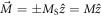 and the field created by the j box at the center of the i box is
  where
where  is the distance between the centers of boxes i and j. Since the applied field is
  the total field at the center of the i box is

If k is the box where  is maximum for all i, then the magnetization of the nanowire switches when
  and
and  .
.
Figure 1. (a) Hysteresis loops for a single nanowire with aspect ratio c/a = 5 using micromagnetic theory (a = 4lex) and our simplified box model with Hcrit = 0 (soft wires) in black and red curves, respectively. A schematic representation of a nanowire with c/a = 5 is shown in the inset. (b) Normalized Hdu as a function of the normalized length of the nanowire, c, for the cases: micromagnetic calculation for a = 4lex (black curve), SW model for a, c ≪ lex (gray dash–dotted curve), and the box model (solid red curve).
Download figure:
Standard image High-resolution imageWhen this criterion is fulfilled, all the boxes of the nanowire switch together. The parameter Hcrit takes implicitly into account the anisotropy of the involved materials. In the case of ideally soft (i.e., no magneto-crystalline anisotropy) nanowires, for simplicity, we assume Hcrit = 0. For the case of hard (large magneto-crystalline anisotropy) nanowires this threshold is taken of the order of saturation magnetization MS, Hcrit ∼ MS (similar to [38] for hard magnetic materials). One could choose Fe and CoPt as soft and hard ferromagnetic materials, respectively, as examples of actual materials.
The weaker magnetostatic field (in absolute value) is at the wire edges [39] (having less neighboring boxes), so Hdu of an isolated soft nanowire is equal to the magnetostatic field at a box at the tip of the wire. This can be calculated as the sum of the magnetostatic fields that all the cells (with a magnetic dipole each one) create to the one at the edge, which can be analytically calculated as

where we have chosen the origin of coordinates at the center of the top box of the nanowire, so the each box is placed at  with i = 1, ..., c/a, and where ϕ(x) and ζ(x) are Polygamma function of second order and the Riemann Zeta function, respectively. This expression can be obtained from equation (1) by setting Ha = 0 and i = 1, where 1 corresponds to the index of the edge box and c/a the number of the boxes in the NW. In figure 1 we analyze the case of an isolated nanowire. Figure 1(a) compares the results of this simple box model for soft nanowires (Hcrit = 0) having aspect ratio c/a = 5 with a micromagnetics simulation [40] (using a = 4lex, where
  and A is the exchange stiffness constant). Note that, although we consider Hcrit = 0, the soft nanowire simulated by the box model has some coercivity due to the shape anisotropy. Namely, at zero-applied field, the total field (now only the magnetostatic field created by all the boxes of the nanowire) has the same direction as the magnetization of nanowire, thus there is no switching despite the Hcrit = 0. Consequently, an extra field of opposite direction is required to overcome the dipolar field and hence induce the switching.
As seen in figure 1(a), the hysteresis loops calculated using micromagnetics and our simple box model are rather similar. Moreover, in the micromagnetics case, the deviation from uniformity field Hdu and the switching field (field at which the magnetization switches its direction) are nearly the same. This allows considering only uniform states during the nanowire magnetization reversal in the box model, and therefore the only parameter that characterizes each hysteresis loop is Hdu. To further verify the validity of our model, in figure 1(b) we plot the normalized deviation from uniformity field Hdu/MS as a function of the aspect ratio c/a of the nanowire using micromagnetics (assuming a = 4lex), and the box model using equation (2). For reference, we also plot the case c, a ≪ lex, corresponding to the classical Stoner–Wohlfarth (SW) case [41], in which the magnetization remains uniform due to the large exchange interaction (only valid if the nanowire has very small dimensions). All calculations converge to the same Hdu = 0 when the nanowire becomes a cube (c = a), because in this case the magnetostatic energy does not depend on the magnetization direction (i.e., no shape anisotropy). For larger c/a, Hdu increases because of the difference in magnetostatic energy between the magnetization parallel and perpendicular to the wire, as predicted in [41]. For all aspect ratios, the largest (negative) Hdu corresponds to the SW limit in which not only the magnetization is uniform, as in the box model, but also the demagnetizing field is. Micromagnetic calculations allow for small deviations of the magnetization (e.g., the formation of 3D flower states at the edges of the wires), therefore decreasing the magnetostatic energy of the nanowire (with respect to the uniform case). This results in a reduction of the switching field with respect to the SW model. Interestingly, the Hdu obtained from the simpler box model roughly follows the trend of the micromagnetic calculations in the whole range of c/a, although it shows a slightly smaller Hdu field since it only considers the field at the edges of the nanowires (where it is weaker). However, the predicted Hdu is reasonably similar to the one calculated with micromagnetics for the whole c/a range. These results justify the use of our simple box model instead of tedious micromagnetic calculations to undertake the analysis of the switching behavior of large arrays of nanowires. Actually, the computation time of both models depends mainly on the evaluation of the magnetostatic field over all the elements and it is thus proportional to the square of their number. Micromagnetic boxes have a typical length ∼lex (or smaller) [42, 43]. Instead, our model assumes that each box is a cube with side Δbox = a. Therefore, there are (a/lex)3 more micromagnetic cells than boxes, and as a consequence the calculation time when using the box model is reduced by a factor (a/lex)6. This implies that while the box model can treat a very large number of wires, the same arrangements turn computationally impossible to be treated by micromagnetics.
Next, we consider regular square arrays of Nx × Ny nanowires, with Nx = Ny = N, separated by a distance d along x and y directions (see sketch in figure 2(b)). Starting from large (positive) applied fields, all the nanowires are initially magnetized in the same direction. Each wire experiences a negative field along z due to the magnetostatic interaction with the rest of the wires, which will depend on the distance between them. In general, the overall magnetostatic field has a maximum (in absolute value) at the central nanowire (assuming N odd); therefore this wire is the one that switches first and determines Hdu of the whole array. In figure 2(b) we show Hdu for an N = 20 arrangement as a function of the inter-wire distance. When the nanowires get closer to each other (d → 0) the switching field is large and positive, in the same direction as the initial magnetization. As the distance between nanowires is increased, their interaction becomes weaker and the deviation from uniformity field becomes negative, tending to the value for an isolated nanowire when d is large (see figure 1(b)). In particular, the magnetic interaction energy between two identical nanowires decreases with d and follows the dipole–dipole interaction dependence 1/d3 for d > 2c (d > 10a) giving negligible long-range interaction values (see figure 2(c)) in agreement with figure 2(b). Similar results were analytically predicted by Guslienko [44] in in-plane magnetized circular cylindrical dot arrays. Interestingly, the shape of the hysteresis loops of the arrays changes considerably with d compared to the one of isolated nanowires. The loops are no longer squared but tilted, as depicted in figure 2(a).
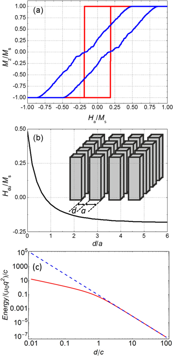
Figure 2. (a) Hysteresis loops for d → 0 (blue) and d → ∞ (red) for N = 20 with aspect ratio c/a = 5. (b) Normalized Hdu for a sample with N = 20 as a function of the separation d. Shown in the inset is a schematic representation of the nanowire arrangement. (c) Normalized magnetic interaction energy as a function of the separation d for the cases of two identical uniformly z-magnetized nanowires with MS (solid red), each one simulated as a pair of magnetic pointed charges of value  separated a vertical distance c, and two identical magnetic dipoles with magnetic moment
  (dashed blue).
Download figure:
Standard image High-resolution imageWe now consider segmented nanowires with a magnetically soft segment (Hcrit = 0) and a hard segment (Hcrit = 3/4MS), both with aspect ratio c/a = 5. The saturation magnetization for the hard segment is MS and for the soft one is 2MS, so when the whole nanowire is uniformly magnetized its overall saturation magnetization is MT = 3MS/2. Shown in figure 3(a) is the loop for a single segmented wire where two segments are infinitely separated along the wire (dz → ∞), so that they do not interact magnetostatically. The hysteresis loop is simply the weighted sum of their individual loops, where the first and second jumps correspond to the reversal of the soft and hard segments, respectively. As can be seen in figure 3(b), for a single segmented wire when the two segments are in close proximity but not in contact (i.e., dz → 0, interacting magnetostatically but neglecting exchange effects), the loop shows a very slightly increase in the switching field of the soft part and an appreciable decrease in the switching field of the hard part with respect to the non-interacting case (dz → ∞). In the interacting case, when saturated in a positive applied field the box that feels a weaker field in the soft part is the one away from the interface. Thus, the field at this cell determines the switching field, which increases only slightly because the field exerted by the hard segment over it is relatively weak and in the same direction as the magnetization. In contrast, once the soft segment has switched, the weaker magnetostatic field over the hard segment is in the interfacial box because of its proximity to the negatively magnetized soft segment, thus, the soft segment induces a field opposite to the magnetization of the hard segment therefore reducing its Hdu.

Figure 3. Hysteresis loops for a soft and a hard segment (see sketches) with c/a = 5, separated (a) an infinite vertical distance (dz → ∞) and (b) at zero vertical distance (dz → 0).
Download figure:
Standard image High-resolution imageTo evaluate the feasibility to obtain multiple well-defined states using segmented wires, arrays of nanowires consisting of a soft and a hard segment (sketched in figure 4(a)) are considered. To optimize the design of the composite material, we analyze in a systematic way the effect of the in-plane distance of the wires in the array, d, and the distance between the soft and hard segments in each nanowire, dz. As can be seen in figure 4(a), when their separation is large (d ≥ 2a) the loop is almost the same as in figure 3(a), with well-established states, thus suitable for applications requiring multiple-states. However, for very small distances the loop radically changes as a consequence of the interactions among the wires and their segments, leading to a rounded shape, not useful for most technological uses. To establish the boundary of d and dz to attain two well-defined states in each hysteresis sub-loop we use the width of the plateau ΔH in the hysteresis loop as a quality parameter. To normalize it, we divide ΔH by its maximum possible value, ΔHmax, i.e., when all segments are completely isolated (see figure 3(a)). In figure 4(b) we show ΔH/ΔHmax for different in-plane (d) and out-of-plane (dz) separations. It can be seen that for inter-wire distances below d/a = 1 the loop has no step, i.e., ΔH/ΔHmax ∼ 0, thus, unusable for most purposes. If we set ΔH/ΔHmax ∼ 0.5 as an indispensable requirement for a stable state, the minimum d suitable for applications would be about 1.5a (for moderate dz). On the other hand, the system is less sensitive to the vertical separation dz between wires. For example, for d = 2a we would need only dz = 0.5a to fulfill the ΔH/ΔHmax ∼ 0.5 criterion. These results indicate that the magnetostatic interaction from vertically separated segments is weaker than that for horizontal ones.

Figure 4. (a) Hysteresis loops for four arrangements of N = 20 arrays of hard/soft segmented nanowires, as shown schematically in the inset. The green curve corresponds to zero separation d = dz = 0, blue to d = dz = a, red to d = dz = 2a, and black to d = dz = 3a. (b) Normalized size of the field plateau, ΔH/ΔHmax, as a function of the normalized separation between nanowires in the horizontal direction, d, and vertical separation between soft and hard segments dz in the vertical direction. Points (1)–(4) correspond to the cases plotted in (a).
Download figure:
Standard image High-resolution image
If the anisotropy of the hard segments is increased, for example by increasing the threshold to Hcrit = MS, we obtain a figure similar to figure 4(b) but with larger values of ΔH/ΔHmax (not shown). The general trends are similar to figure 4(b) although the data is shifted to the left and down, that is, for d = 2a and dz = 0.5a we obtain ΔH/ΔHmax ∼ 0.7. Consequently, to fulfill ΔH/ΔHmax ∼ 0.5 criterion only d = 1.5a and dz = 0.25a would be necessary for this higher anisotropy case. Hence, in principle, designing multi-level nanowires with higher anisotropies of the hard counterpart would be desirable to increase the magnetic stability while safely operating the system. However, the maxim field available from the electromagnetic coils to establish the orientation of the hard layer would set the limit for the maximum allowable anisotropy.
In conclusion, we have presented a simple but powerful model to describe the magnetization switching of large arrays of segmented nanowires. Our model is capable of predicting the distances over which nanowires do not interact appreciably with their neighbors (horizontal separation d > a). At the same time we demonstrate that nanowires made of segments of different coercivity and saturation magnetization can be used to attain antiparallel or parallel magnetic alignment, as required in magnetic sensors based on the GMR effect and other applications based on multiple-states. Thus, the model can become a useful tool to efficiently design future optimized spin-valve like sensors or even other applications, such as high-density multi-level recording media or magnetic encoders.
We acknowledge the support from the 2014-SGR-1015 and 2014-SGR-150 projects of the Generalitat de Catalunya, the MAT2012-35370 and MAT2014-57960-C3-1-R projects from the Spanish Ministerio de Economía y Competitividad (MINECO)-the latter cofinanced by the 'Fondo Europeo de Desarrollo Regional' (FEDER)-, the SPIN-PORICS 2014-Consolidator Grant (Grant Agreement 648454) from the European Research Council (ERC), and the MANAQA project (grant agreement 296679) from the European Community's Seventh Framework Programme (FET-Open/FP7/2007-2013). AS acknowledges funding from an ICREA Academia award. EP acknowledges the Spanish Ministerio de Economía y Competitividad (MINECO) for the 'Ramon y Cajal' contract (RYC-2012-10839). ICN2 acknowledges support from the Severo Ochoa Program (MINECO, Grant SEV-2013-0295).