


Abstract
We propose a scheme of band engineering by means of staggered electric potential, antiferromagnetic exchange field and intrinsic spin–orbit coupling for electrons on a honeycomb lattice. With fine control on the degrees of freedom of spin, sublattice and valley, one can achieve a topological state with simultaneous non-zero charge and spin Chern numbers. With first principles calculations, we confirm that the scheme can be realized by material modification in perovskite G-type antiferromagnetic insulators grown along the [111] direction, where Dirac electrons from d orbits are achieved on an atomic sheet of a buckled honeycomb lattice. In a finite sample, this state provides a spin-polarized quantum edge current, robust to both non-magnetic and magnetic defects, with the spin polarization reversible by electric field, and is thus ideal for spintronics applications.
Export citation and abstract BibTeX RIS

Content from this work may be used under the terms of the Creative Commons Attribution 3.0 licence. Any further distribution of this work must maintain attribution to the author(s) and the title of the work, journal citation and DOI.
GENERAL SCIENTIFIC SUMMARY Introduction and background. The quantum Hall effect (QHE), discovered by von Klitzing in 1980, has been revealed as a manifestation of the topological nature of the Bloch wavefunction, labeled by the Chern number. A breakthrough in exploring new topological materials took place when Kane and Mele clarified in 2005 that quantum spin Hall effect (QSHE) can be achieved in graphene by including spin–orbit coupling (SOC). It turned out that the gap opened by SOC in graphene is very small, which makes detection of QSHE hopeless. QSHE was then predicted theoretically and realized experimentally in a HgTe quantum well with stronger SOCs.
Main results. We propose the insertion by MBE of one layer of La2Au2O6 into a host perovskite Mott insulator LaCrO3 grown in the [111] direction (see the figure). d electrons of Au hop on a buckled honeycomb lattice under the G-type antiferromagnetic (AFM) exchange field established by the parent material. The combination of AFM field, the sizable spin–orbit coupling, and the staggered electric potential generated by the electric field along the [111] direction, taking advantage of the buckled structure, tunes the energy gaps at the two valleys. When the band is inverted at one valley with a specified spin, a novel topological state can be achieved, characterized by simultaneously nonzero charge and spin Chern numbers. In a finite system, an edge current with spin polarization appears, breaking the chiral symmetry.
Wider implications. This work proposes a class of perovskite materials that exhibit a new topological state with spin-polarized edge current stable even up to high temperatures. This novel topological phase has great potential for spintronics applications.
 Figure. Schematics for host perovskite material LaCrO3 in the [111] direction (blue slabs) with one atomic layer of La2Au2O6 (golden layer) inserted, where the Au atoms (golden balls) form a buckled honeycomb lattice.
1. Introduction
The discovery of the quantum Hall effect by von Klitzing opened up a new chapter in condensed matter physics. It was revealed [1, 2] that the integer coefficient in Hall conductance is nothing but the Chern number labeling the topological property of the electron wavefunction. Since then, exploring the possible topological states has been one of the main driving forces in the study of condensed matter physics [3–10].
The breakthrough took place when Kane and Mele clarified that electrons on graphene, a two-dimensional honeycomb lattice of carbon atoms, open a gap by spin–orbit coupling (SOC) and achieve a topologically non-trivial state called the quantum spin Hall effect (QSHE) [4]. It turned out that in graphene the intrinsic SOC is very small, which makes detection of QSHE hopeless. QSHE was then predicted theoretically [5] and realized experimentally in a HgTe quantum well with strong SOC [6].
As the common homebase for both the Kane–Mele model [4] and the spinless Haldane model [3], the honeycomb lattice has a unique role in understanding the topological property of electron systems. It may be illustrative to summarize its electronic structure by paying attention to the Berry curvature configuration [11]. There are two sites in the unit cell of the honeycomb structure. With nearest-neighbor hopping, the electronic valence and conduction bands touch linearly and thus form Dirac cones at two inequivalent k points, K and K', located at the corners of the Brillouin zone. It is important to observe that Bloch wavefunctions exhibit opposite chiral features around K and K', characterized by opposite Berry curvatures, which establishes the special position of the honeycomb lattice in exploring topological states.
With time-reversal symmetry, the Berry curvatures in spin-up and spin-down channels overlap, as shown in figure 1(a). Introducing intrinsic SOC opens a gap at the two Dirac cones, and flips Berry curvatures at K in the spin-up channel and at K' in the spin-down channel preserving time-reversal symmetry, which results in the Berry curvature configuration in figure 1(b), characterizing the QSHE state [4]. One can further flip the Berry curvatures at K in both the spin-up and spin-down channels, yielding the configuration in figure 1(c) (a topologically trivial state), by a field conjugate to the valley degree of freedom such as the polarized field [12–15]. With an additional staggered electric field, which can be realized in silicene with a buckled honeycomb lattice in terms of a uniform electric field [16], Ezawa could flip the Berry curvature at K in only one spin channel, resulting in figure 1(e) characterized by simultaneous non-zero charge and spin Chern numbers [15] (see also [17–19]). Band engineering is based on full control on the degrees of freedom of spin, valley and sublattice, taking advantage of the intrinsic SOC. To finish the discussion here, we note that the Berry curvature configuration in figure 1(d) corresponds to the quantum anomalous Hall effect (QAHE) [18–23].
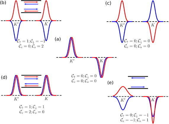
Figure 1. Schematic diagrams for possible configurations of Berry curvatures and Chern numbers for insulating states on a honeycomb lattice: (a) pristine honeycomb lattice, (b) QSHE, (c) trivial state with broken time-reversal symmetry, (d) QAHE and (e) topological state with simultaneous non-zero charge and spin Chern numbers. Curves above/below the horizontal dashed line are for positive/negative Berry curvatures, and red/blue for spin up/down channels, each of area 1/2 associated with a meron structure. Edge currents are displayed in the insets in (b), (d) and (e) for topologically non-trivial states. C↑, C↓, Cc and Cs are up-spin, down-spin, charge and spin Chern numbers, respectively.
Download figure:
Standard image High-resolution imageIn this paper, we note that in the presence of intrinsic SOC, a staggered magnetic field plays a similar role as provided by the polarized light proposed by Ezawa [15]. Since the staggered magnetic field can be realized by antiferromagnetic (AFM) insulators, compact and stable devices based on the topological state in figure 1(e) are possible as compared with the photo-assisted scheme.
As material realization of our idea, we focus on d-electron systems in perovskite structure [24]. First, we choose a perovskite insulator ABO3 with G-type AFM order on the magnetic B atoms. As first discussed by Xiao et al [9], along the [111] direction B atoms form a stacking of the buckled honeycomb lattice, which can be grown by cutting-edge molecular beam epitaxy (MBE) with atomic precision [25]. During the growing process, a single buckled honeycomb layer of B atoms is replaced by that of non-magnetic B' atoms, where the element B' is chosen conjugate to B in order to form a d8 configuration. For B'-d electrons on the single buckled honeycomb lattice, intrinsic SOC becomes sizable, a uniform electric field induces a staggered electric potential for the two sublattices, and the G-type AFM order on B atoms on the two sides provides an AFM exchange field. The material design makes the magnetic field of pure exchange character, which avoids possible stray fields from permanent ferromagnets. We have checked successfully our idea by performing first principles calculations for several materials. In transition metal perovskites, we found intrinsic SOC of several tens of meV, which is larger than that in silicene in magnitude by one order, and makes the new topological state available at room temperature.
2. Effective model and phase diagram
Let us illustrate our scheme based on the four-band Hamiltonian for electrons on a buckled honeycomb lattice under an AFM exchange field and a uniform electric field perpendicular to the plane,4

around the two inequivalent K and K' points where the z-axis is taken along the [111] direction of perovskite structure; σ's are Pauli matrices for the sublattice, and τz = ± 1 and sz = ± 1 are binary degrees of freedom referring to valley and spin. The first two terms come from the nearest-neighbor hopping similar to that in pristine graphene (see footnote 4); the third term is for the intrinsic SOC with a positive coupling coefficient λ > 0 by definition, which can be large due to the heavier host transition metal atom and the buckled structure; the fourth term is induced by a uniform electric potential on the buckled structure, and the last term is the AFM exchange field. The chemical potential is set to zero, and all energies are measured in units of the nearest-neighbor hopping integral in this work. As will be shown later, this model Hamiltonian describes the low-energy physics of transition metal oxides with perovskite structure grown along the [111] direction.
We reveal behaviors of the system below upon tuning the electric potential V while the M field and λ are fixed, corresponding directly with our material design and experimental manipulation. For 0 < M < λ, the gaps are topologically non-trivial for both spin-up and spin-down channels for V =0, characterizing the QSHE state (see figure 1(c)). As illustrated in figure 2(b), when V increases, the gap for the spin-up channel shrinks, closes and reopens at the K' point (τz = −1) for V =λ − M. This quantum phase transition turns the spin-up channel into a trivial state, while the spin-down channel remains non-trivial. This insulating state exhibiting a non-trivial gap in only one spin channel is different from other topological states such as QSHE and QAHE [15]. When V increases further, the gap for the spin-down channel shrinks, closes and reopens at the K point (τz = 1) for V =λ + M, which makes the spin-down channel trivial as well, and the system transforms to a trivial insulating state via a second quantum phase transition.
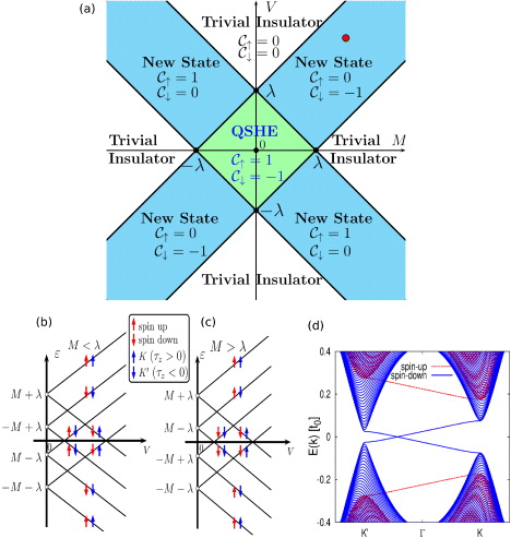
Figure 2. (a) Phase diagram for staggered electric potential V and AFM field M, with presumed positive intrinsic SOC λ > 0; (b) and (c) schematic diagram for energy level crossing upon electric field tuning for M < λ and M > λ; (d) band structure for an N = 100 zigzag ribbon of the honeycomb lattice with V =0.25, M = 0.2 and λ = 0.1 (red dot in (a)).
Download figure:
Standard image High-resolution imageFor M > λ, the system exhibits trivial gaps in both the spin-up and -down channels for V =0 (see figure 1(c)). As seen in figure 2(c), when V increases, the gap for the spin-down channel shrinks, closes and reopens at τz = −1 for V =M − λ, which brings the spin-down channel into a topological state. When V increases further, the gap in the spin-down channel shrinks, closes and reopens at τz = 1 for V =λ + M, which drives the system back to a trivial insulator state.
Based on the above analysis, we can compose the full phase diagram as displayed in figure 2(a) by symmetry considerations. The new topological state is realized when the absolute values of the three fields |V |, |M|, and |λ| form a triangle, which indicates clearly that the intervening among the three degrees of freedom, σz, τz and sz, is crucial for the new topological state. A typical band structure for a zigzag ribbon of the buckled honeycomb lattice is displayed in figure 2(d); there are two edge states crossing the Fermi level that are localized at the opposite edges (see figure 1(e)). The present phase diagram is similar to that by Ezawa [15], except that states with the same Chern numbers lie in diagonal directions in the present one, while locating in the same half spaces in that by Ezawa [15], due to the difference of controlling fields in the two Hamiltonians.
3. Material realization
In perovskite ABO3 material shown in figure 3(a), A and B form two penetrating simple cubic lattices. The octahedron cage formed by six oxygens around the transition metal B generates the doublet eg and triplet t2g orbits of the d electrons. In the [111] direction, a simple cubic structure can be viewed as a stacking of buckled honeycomb lattices, as shown in figures 3(b) and (c). In the new coordinate, intrinsic SOC appears between the two eg orbits. In regard to material synthesis, recent developments in the laser MBE technique permit one to grow perovskite structure along the [111] direction with atomic precision [25]. All these make the d electrons in perovskite structure a very hopeful platform for realizing topological states, as illustrated first by Xiao et al [9].
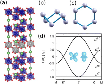
Figure 3. (a) A six-layer ABB'X perovskite with one layer of B (blue) replaced by B' (gray). (b) and (c) Side and top views of the buckled honeycomb lattice formed by B' cations. (d) Non-interacting tight-binding band structure of the eg system, where each band is labeled with the corresponding electron configuration if it is occupied. The inset shows the two eg orbits of B'.
Download figure:
Standard image High-resolution imageMany transition metal oxides with perovskite structure are known as wide-gap AFM insulators. A subgroup of these materials presumes the so-called G-type AFM order where spins align antiferromagnetically in the two sublattices of the buckled honeycomb lattice. This is the playground where we perform material design and field manipulation to realize a topological state with our scheme. We replace one buckled layer of B by a non-magnetic element B', and obtain B'-d electrons on a single layer of the buckled honeycomb lattice, which experience an AFM exchange field from the G-type AFM order of the host material ABO3.5
There is a gap (10 Dq) between the eg and t2g orbits, which drops t2g orbits from the low-energy physics. In each unit cell, two B' atoms contribute totally four eg orbits. The band structure for these four orbits is shown in figure 3(d) based on a tight-binding Hamiltonian with the hopping integrals given by the Slater–Koster formula. One finds two flat bands and two dispersive bands crossing each other. Xiao and co-workers [9, 18, 19] focused on the flat band and developed an interesting scenario for possible topological states based on strong electron correlations by using the d7(t62ge1g) configuration. Here we concentrate on the two dispersive bands by taking d8(t62ge2g) systems for which the Fermi level is around their crossing point.
In order to verify the above picture, we have performed first-principles calculations on the host material LaCrO3 with one layer of La2Ag2O6 or La2Au2O6 inserted, which realizes a d8(t62ge2g) system on the buckled honeycomb lattice. The electric field is V =0 since, on the one hand, it is the basis state on which tuning by an electric field is performed and, on the other hand, the results thus obtained are pedagogical for the underlying physics. The supercell used in the calculations contains six layers with a configuration of (La2B'2O6)/(La2B2O6)5. The calculations are performed by using density functional theory within the generalized gradient approximation (GGA) approach in the parameterization of Perdew et al [26] for exchange–correlation as implemented in the Vienna Ab Initio Simulation Package [27]. The bulk lattice constant is set to 3.85 Å for LaCrO3 and atoms are allowed to relax inside the supercell. The on-site Coulomb interactions of the 3d electrons of Cr are treated by Dudarev's method with an effective U value [28], Ueff = U − J = 5.4 eV. The results displayed are based on the 6 × 6 × 1 momentum space-mesh and the cutoff energy 440 eV, and the convergence of results is confirmed by using several sets of parameters.
The band structures of LaCrAgO and LaCrAuO obtained from GGA + U + SOC calculations are displayed in figures 4(a) and (b). The bands in black are mainly from the parent material LaCrO3 with a large gap of 3 eV, characterizing a Mott insulator. The bands in blue inside this large Mott gap are contributed by the eg electrons of Ag3+ and/or Au3+, with two almost flat bands and two dispersive bands, as discussed above and displayed in figure 3(d). Gaps are opened at K and K' since the Dirac electrons in figure 3(d) for the tight-binding model now feel the AFM exchange field from LaCrO3 and SOC. As can be seen from equation (1) with V =0 and figure 2(c), the two gaps are given by 2(M + λ) and 2(M − λ). Coupling of the valley degree of freedom to the AFM order was recently discussed by Li et al [29] in manganese chalcogenophosphates.
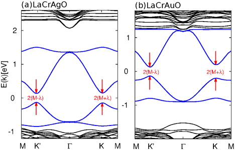
Figure 4. Band structures based on first-principles calculation on LaCrAgO and LaCrAuO with a super unit cell (A2B'2O6)/(A2B2O6)5 along the [111] direction.
Download figure:
Standard image High-resolution imageFrom the two gaps at K and K', we figure out that M = 0.141 eV and λ = 7.3 meV for LaCrAgO, and M = 0.166 eV and λ = 32.91 meV for LaCrAuO. We have also calculated several other possible materials and the results are summarized in table 1. In all these systems, the obtained AFM field dominates the gap since M > λ, which indicates that the pristine state (namely V =0) corresponds to the configuration of Berry curvatures in figure 1(c) associated with a topologically trivial spin-density wave state. As discussed above and summarized in figure 2(a), upon increasing the staggered electric potential, the gap at one valley in one spin channel is closed first, and then a non-trivial gap is reopened that is dominated by SOC, driving the system into the new topological state in figure 1(e). As the maximal non-trivial gap is given by 2λ, the results from first-principles calculations suggest that a topological material may be realized at room temperature. A typical electric field to realize the new topological state is of the order of 0.1 V Å−1.
Table 1. Parameters for AFM order and SOC fit from GGA + U + SOC calculation. For KNiInF and KNiTlF the electronic configurations of In2 + and Tl2+ are 5s1 and 6s1.
| Field (meV) | LaCrAgO | LaCrAuO | LaFeAgO | LaFeAuO |
|---|---|---|---|---|
| M | 141 | 166 | 541 | 467 |
| λ | 7.30 | 32.91 | 7.31 | 33.52 |
| KNiPdF | KNiPtF | KNiInF* | KNiTlF* | |
| 625 | 504 | 290 | 235 | |
| 11.38 | 33.40 | 5.05 | 18.58 |
4. Possible applications
This new topological state, likely available at room temperature, is ideal for spintronics applications, since it provides a spin-polarized quantum edge current, robust to both non-magnetic and magnetic defects, with the spin polarization tunable by inverting electric field.
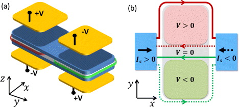
Using two copies of the new topological state, one can realize a 'composite QSHE insulator'. As shown in figure 5(a), we fabricate two pairs of electrodes (golden) with opposite bias voltages. The two patches exhibit states with opposite chiralities and spins. Spin Hall conductance can be measured based on this device. As shown in figure 5(b), when a positive spin current Is is injected from the left electrode, the out-going spin-up current flows from the left electrode along the top edge of the upper patch (upturned red solid curve), while the in-going spin-down current flows into the left electrode along the straight line between the two electrodes (solid green line), which results in zero charge current. Because charge current flows only on the top edge and cumulates charges there, a Hall voltage drop can be detected between the top and bottom edges of the device. As compared with the QSHE realized before, even a time-reversal symmetry-broken perturbation, e.g. a magnetic field or magnetic impurities, cannot backscatter the counter charge currents with spin up and down at the center of the device, since the charge currents are now distributed in different patches as shown in figure 5(b).
Figure 5. Device for a 'composite QSHE' insulator formed by two copies of the new topological state.
Download figure:
Standard image High-resolution image
5. Discussion
The present topological state is robust against Rashba SOC [22, 23], which, although small, should be present since both the electric field and the buckling structure of the honeycomb lattice break the inversion symmetry. It is known that in graphene the non-trivial band gap closes for λR > λ and the QSHE will be destroyed [4] due to the mixing of the two spin channels by Rashba SOC. In the new topological state with, for example V =M > 0 a gap of 2(2M − λ) is opened in the spin-up channel whereas the gap in the spin-down channel is 2λ. Since M ≫ λ as shown in table 1, even a Rashba SOC stronger than the intrinsic one λR ≳ λ cannot close the gap by mixing the two spin channels. For the same reason, other spin mixing mechanisms such as coupling between electron spin and nuclear spin polarization [30] are not able to destroy the present topological state. There are also other studies showing that in QSHE a random Rashba SOC together with electron interactions will localize the helical edge states [31, 32]. In the present case, however, there is only one edge state at each edge and the only electron interaction is the forward scattering interaction that leads to a trivial velocity renormalization, not to localizing the edge state.
Acknowledgments
XH is grateful to Masashi Tachiki and Seiji Miyashita for helpful discussions. This work was supported by WPI Initiative on Materials Nanoarchitectonics, MEXT of Japan and Grants-in-Aid for Scientific Research (numbers 22540377 and 25400385), JSPS, Innovative Area 'Topological Quantum Phenomena' (number 25103723), MEXT of Japan, and partially by CREST, JST. QFL was also supported by NSFC under grant number 10904092.
Around the time of completion of our paper, we became aware of recent work by Ezawa [33], addressing similar physics. In his work, the staggered magnetic field is generated by two ferromagnets on the two sides of the silicene layer.
Footnotes
- 4
For the d8 system where the electronic structures involve two degenerated eg orbits, one can still obtain an effective H0 by reducing a four-band Hamiltonian into a two-band one using kp perturbation theory (for more details see the supplementary material, available from stacks.iop.org/NJP/15/063031/mmedia).
- 5
Actually there are two magnetic configurations that have similar energies. From our first-principles calculations, we found that the one that induces the desired AFM magnetization in the AB'O3 layer always has a lower energy (see the supplementary material, available from stacks.iop.org/NJP/15/063031/mmedia).