
Abstract
We investigate the voltage–current characteristics of a superconductor–insulator–ferromagnet heterostructure, where the insulating layer contains pinhole-defects. The superconducting layer exhibits multiple voltage jumps that are hysteretic with the current sweep direction. This characteristic of the resistive state is due to pinholes that induce local, distinct, coupling regions between the superconducting and ferromagnetic layers which may generate phase-slip lines or vortex channeling. These findings point to a magnetically driven design of a superconductor memristor. Concomitantly, the junctions display both absolute and differential negative resistances below the superconducting critical temperature and current. This anomalous behavior is analyzed using a circuit approach and is attributed to current passing through pinholes within the insulating layer. These two unique effects, which stem from the special topology of the pinholes-governed interface can be applied in superconductor-based switches and memory devices.
Export citation and abstract BibTeX RIS

Original content from this work may be used under the terms of the Creative Commons Attribution 4.0 license. Any further distribution of this work must maintain attribution to the author(s) and the title of the work, journal citation and DOI.
1. Introduction
In a quasi one-dimensional superconductor, phase fluctuations can cause phase slippage in phase-slip centers that lead to dissipation below the superconducting critical parameters [1, 2]. This is observed as a step-structure behavior of the voltage–temperature V(T) and voltage–current V(I) curves. Similar voltage jumps also appear in wide superconducting films (i.e., wide relative to the penetration depth) due to phase-slip lines (PSLs) or vortex channeling or streets [3–7]. PSLs are considered the two-dimensional analogue to phase-slip centers [8], describing time-periodic suppressed superconductivity along a line perpendicular to the current direction that generates non-equilibrium quasiparticles [3]. Vortex streets are spontaneously nucleated pairs of vortices that move perpendicular to the current direction [3, 9, 10]. These pairs are generated by the current-induced magnetic field, nucleate at the edges of the superconductor and annihilate at its center its center [4, 6]. Along with these phenomena, one should note that when measuring a V(I) curve, the characteristic currents where voltage jumps occur can be hysteretic with respect to the current sweep direction due to self-heating.
Control over phase-slip processes and the kinematic vortices can be achieved via artificially-designed pinning centers that can affect the superconducting order parameter landscape [11, 12]. In addition to the basic scientific interest of studying dissipative effects in superconducting materials, such control may be used for superconductor-based electronics. In this work we demonstrate a method for achieving control over the spatial occurrence of phase-slip processes or the related vortex kinematics, by locally modulating the proximity effect via pinholes within a thin layer of aluminum-oxide (AlOx ) that separates superconducting and ferromagnetic films. The resulting V(I) characteristics exhibit voltage jumps and a unique memristor-type behavior, which is related to the pinholes in the AlOx layer.
We also observe another intriguing phenomenon related to the pinholes: a sign-changing electrical resistance (negative to positive) in the V(I) characteristics of the superconductor. Negative resistance can describe both negative differential resistance,  , and absolute negative resistance where
  . In a device showing current-controlled negative differential resistance, the voltage across the terminals will decrease when the current through it grows, until some transition current above which the voltage increases. It is known that negative differential resistance can also appear in four-point transport measurements of crossed-wire junctions under some condition of the ratio between the wires resistance and the junction resistance [13], as observed in a twisted superconducting carbon nanotubes yarns [14] and in vanadium nanowires [15].
Here, we perform electrical transport measurements on hybrid superconductor–insulator–ferromagnet (S–I–F) and superconductor–ferromagnet (S–F) crossbar heterostructures formed of a superconducting strip placed perpendicularly on an array of ferromagnetic strips with or without an intermediate insulator layer (i.e., S–I–F or S–F, respectively). The superconducting layer exhibits voltage steps below the global critical current that are hysteretic with the current sweep direction. Concomitantly, V(I) characteristics obtained on the S–I–F junctions display both absolute and differential negative resistances below the superconducting critical current and temperature, an effect that is not observed in the S–F junctions. We argue that the negative resistance is associated with currents passing through discrete pinholes in the insulating layer in conjunction with the measurement configuration, as described below.
2. Methods
The devices were fabricated on 5 mm × 5 mm single crystal silicon substrates with a 250 nm thick thermally oxidized surface layer using photolithography with two lift-off steps. In the first step, nine parallel ferromagnetic strips of width 100 μm and length 4 mm were defined, spaced 100 μm apart. The ferromagnetic strips consisted of an Al(3 nm)/Pt(5 nm)/[Co(0.8 nm)/Pt(1 nm)]×8] structure, deposited by DC magnetron sputtering in 1 Pa of Ar in an ultrahigh-vacuum chamber with a base pressure of less than 10−6 Pa. The top 3 nm thick layer of Al was oxidized (AlOx ) in 100 Pa of static O2 for 1 h before the second step where a 25 nm thick orthogonal superconducting strip of Nb was defined. The Nb was deposited by magnetron sputtering and a 3 nm thick layer of Pt capped the structure. Nine cross-wire junctions were fabricated over an area of 100 × 100 μm2. A Control device without AlOx layer was also fabricated using the same protocol. Note that the ferromagnetic and superconducting layers were deposited simultaneously for all devices, with or without the insulating layer, to ensure that the F-layers and S-strip in all devices are identical.
Current-biased electrical measurements were performed in a 4He pulse-tube dry cryostat fitted with a superconducting solenoid. The V(I) characteristics of the superconducting layer and devices (S–F and S–I–F) were measured using a continuous current source (Keithley 2400) and a nanovoltmeter (Keithley 2182) in a four-point probe configuration (figures 1(c) and (d)).
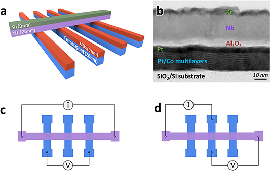
Figure 1. (a) A schematic diagram of the S–I–F device: a 100 μm-wide Pt/Nb strip (top) and multiple parallel strips of a ferromagnetic multilayer of Co/Pt with an AlOx surface (bottom). (b) Bright-field cross-sectional HR-TEM micrograph of the layered structure in the junction region. The scale-bar has a length of 10 nm. (c) and (d) Configurations of the four-point probe transport setup to measure V(I) characteristics of the superconducting strip (c) and of a S–I–F junction (d).
Download figure:
Standard image High-resolution imageOur previous experience fabricating AlOx tunnel junctions shows [16–18] that the thickness and microstructure of the Nb base layer, as well as the thickness and uniformity of the Al base layer, are crucial factors for achieving a homogeneous tunneling current through the AlOx layer (avoiding shorts such as pinholes). Importantly, the AlOx barrier inherently contains pinholes unless it is capped with a thin layer of Al that enables the formation of a genuine tunneling barrier. The deposition of this Al cap onto AlOx enables oxygen and aluminum atoms to inter-diffuse, effectively sealing any pinholes and creating a uniform, high-resistance barrier of AlOx . In our present experiment, we intentionally excluded the top layer of Al in order to preserve the presence of pinholes. This deliberate exclusion allows us to investigate and analyze the behavior and impact of these pinholes in our experimental setup. Moreover, we have measured the resistance of S–I–F junctions (above TC) where the thickness of the AlOx layer was either 2 nm or 3 nm. We found that the ratio between the resistances of the 3 nm and 2 nm thick AlOx samples is ∼1.7. This ratio is much too small to be accounted for by a genuine tunnel barrier, thus providing a strong evidence for a leaky barrier, namely, the existence of pinholes.
3. Results and discussion
A schematic diagram of the S–I–F device is presented in figure 1(a) along with a cross-sectional high-resolution transmission electron microscope (HR-TEM) micrograph of the structure (figure 1(b)) that verifies the thicknesses of the different layers detailed in the methods section. A photograph of the device is presented in the supporting information (figure S1). The S–I–F device exhibits a critical temperature ( ) of about 6 K (see figure S2 in the supporting information), whereas the S–F device had a
  of about 6.2 K (measured using the contact configuration depicted in figure 1(c)). The difference is likely due to variations in the fabrication and post-fabrication treatment of the two samples, which is more elaborate for the former device.
To measure the V(I) characteristics of the superconducting layer, V was measured between two parallel F electrodes while driving a current through the S layer (figure 1(c)). I was swept in two directions: upwards (negative to positive values) and downwards (positive to negative values). As a control, we measured the voltage between two points directly bonded to the Pt layer on Nb, as opposed to the F contacts. Both configurations show matching V(I) characteristics (figure S3), indicating that the ferromagnetic nature of the voltage contacts was not the cause of the stepped hysteretic structures described below.
Both devices, with and without the AlOx
, show a switching current ( ) that marks the transition from a partially superconducting state to the global normal state, and a retrapping current (
 ) that marks the reverse transition. The difference between these two currents is seen as a hysteresis loop around 7 mA when sweeping the current upwards and downwards (figures 2(a) and (b)). This hysteresis stems from self-heating of the Nb, due to transitioning to the global normal state where a high current passes through the normal regions, dissipating Joule heat. This is also evident from the temperatures recorded during the measurements, showing an increase in temperature above
  (see insets in figures 2(a) and (b)).

Figure 2.
V(I) characteristics of the superconducting layer in the device without (a) and with (b) the insulating layer at 2 K and 3 K, correspondingly. Colors represent upwards (black) and downwards (red) current sweep directions, as indicated by the arrows. Insets: Temperatures of the device recorded simultaneously with the transport measurements. (c) and (d) Magnification of the curves in panels (a) and (b), respectively. At the low current regime, an additional 'inner' hysteresis loop is visible only in the device with the insulating layer. The location of the first voltage jump for the case of positive or negative currents is labeled  or
or  , respectively, and marked with arrows in panel (d).
Download figure:
Standard image High-resolution imageWe note that below the switching current,  , the superconducting Nb continues to be dissipative (in both the S–F and S–I–F devices) and so we term this state as partially superconducting, i.e., that part of the layer is not superconducting. The first transition from zero-voltage to finite-voltage occurs at a much lower current (
 ∼ 0.2–0.5 mA). This is in contrast to what is typically observed in a homogeneous superconductor where only one voltage jump occurs between a global superconducting (zero resistance) state to a global normal state in the upwards current-sweep direction, and only one down-step occurs to the zero-resistance state at
  <
<  , constituting only one hysteresis loop. In our case, above
  the superconductor enters an intermediate state where some regions can no longer support the high current without dissipation. Within this intermediate state a second hysteresis loop appears only in the S–I–F devices (figure 2(d)), exhibiting multiple voltage jumps. The jumps are reproducible for the same temperature, occurring at the same current values for each repetition (see figure S4), but are hysteretic with the magnetic field (figures 4 and S4). These jumps are most apparent when sweeping the current from zero to
  , but they also weakly appear when sweeping the current back to zero from
  (see figure S5). Importantly, the inner hysteresis loop does not appear in devices without the AlOx
layer (figure 2(c)), and also when there is no junction between the voltage probes in the S–I–F device (figure 5). These latter observations suggest that the origin of the voltage steps is related to the pinholes scattered in the AlOx
layer of the S–I–F junctions. This is further supported by the fact that increasing the distance between the voltage contacts, thus measuring voltage over a longer distance and over more S–I–F junctions, increases the number of voltage steps (figure S6).
(see figure S5). Importantly, the inner hysteresis loop does not appear in devices without the AlOx
layer (figure 2(c)), and also when there is no junction between the voltage probes in the S–I–F device (figure 5). These latter observations suggest that the origin of the voltage steps is related to the pinholes scattered in the AlOx
layer of the S–I–F junctions. This is further supported by the fact that increasing the distance between the voltage contacts, thus measuring voltage over a longer distance and over more S–I–F junctions, increases the number of voltage steps (figure S6).
As mentioned in the introduction, multiple voltage jumps are typical of current-biased wide two-dimensional superconductors where voltage jumps are interpreted as a consequence of spatially localized PSLs or vortex streets [3], inducing a vortex channeling effect [9]. The fact that the voltage jumps were not observed in the S–F heterostructures, where the proximity effect between the S and F layers in the junctions is expected to be stronger, is quite puzzling. This may point to the role of pinholes in the AlOx layer that allows some electrical contact between the S and F layers and some charge flow between the two layers. In a somewhat related structure, Kalcheim et al observed voltage steps attributed to vortex channeling caused by inhomogeneous quasiparticle distribution that forms due to charge transfer through the pinholes [6]. These regions can, in turn, induce PSLs.
With increasing temperature or increasing out-of-plane magnetic field, both  and
and  decrease (figure 3).
  decreases slower and thus the width of the hysteresis narrows with increasing applied magnetic field and temperature. This effect occurs also for in-plane applied magnetic field (figure S7).
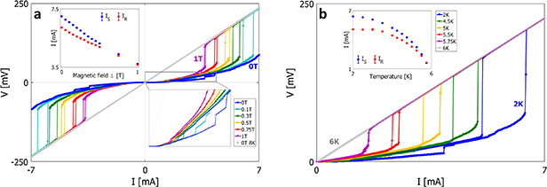
Figure 3. (a) V(I) characteristics at 3 K of the superconducting layer in a S–I–F device under different (labeled) out-of-plane magnetic fields. Bottom inset: zoom-in on the first hysteresis at low currents. Top inset: magnetic-field-dependence of  and
and  . (b) V(I) characteristics of the superconducting layer in a S-I-F device at different temperatures (labeled). Inset: temperature-dependence of
  and
and  .
.
Download figure:
Standard image High-resolution imageThe inner hysteresis loop also narrows and shifts to lower currents with increasing magnetic field (inset of figure 3(a)) and temperature (figure 4). In particular, the current where the first voltage jump takes place,  , and the jump magnitude reduce with increasing temperature and magnetic field, and the same holds for
  . Interestingly,
  and
and  are non-symmetric for positive and negative magnetic fields (figures 4(b) and (c)). In addition, for small magnetic fields (smaller than ∼0.003 T, correlated to the saturation field of the ferromagnetic layer as measured by SQUID magnetometry, see figure S8)
  and
and  are hysteretic with the magnetic field sweep direction, most pronouncedly seen for the zero magnetic field data-points in figures 4(b) and (c). These effects of the magnetic field imply that the hysteretic nature of the voltage jumps is not only a result of local heating in the superconducting layer. Particularly,
  and
and  depend on the magnetic field sweep direction only below the saturation field of the F layer. This is reasonable since above the saturation field the magnetic order in the F does not depend on the sweep direction. This indicates a connection between the magnetic properties of the F layer and the voltage jumps, where the coupling between the F and S layers is modulated by the pinholes-network in the AlOx
layer.
depend on the magnetic field sweep direction only below the saturation field of the F layer. This is reasonable since above the saturation field the magnetic order in the F does not depend on the sweep direction. This indicates a connection between the magnetic properties of the F layer and the voltage jumps, where the coupling between the F and S layers is modulated by the pinholes-network in the AlOx
layer.

Figure 4. (a) V(I) characteristics of the superconducting layer focusing on the 'inner loop' regime at various temperatures (labeled). The locations of the voltage jumps shift to lower currents as the temperature rises. The location of the first voltage jump (termed  and marked in figure 2) is plotted as a function of temperatures in the inset. (c) and (d) The dependence of
  and
and  on an out-of-plane magnetic field (at 3 K) is different when the field is swept up from negative to positive values (b) or swept down (c).
Download figure:
Standard image High-resolution imageTo confirm that the origin of the inner hysteresis loop is related to the S–I–F junctions, we performed measurements in a configuration where there is no such junction between the voltage probes, that were directly bonded to the Pt layer on top of the Nb (see figure 5). Indeed, the inner hysteresis loop vanished; but there are other significant changes in the V(I) curve compared to those seen in figures 2(b) and (d), measured on the same device and at the same temperature (3 K). First, the transition from the zero voltage (global superconducting) state takes place at a much higher current bias (2 mA compared to 0.4 mA), and the transition is sharp (see upper inset of figure 5), as opposed to the step-structured transition see in figure 2. Moreover, now we observe the common behavior of a retrapping transition at a current lower than the switching current. The second transition, from the partially superconducting state to the global normal state at higher current bias, differs from that in figure 2 by the fact that the retrapping part (onset at ∼6.2 mA) takes place in two steps, while the switching ( ∼ 6.8 mA) is sharp, as in figure 2(b). This may be due to local inhomogeneities in the Nb film.
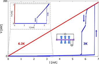
Figure 5. V(I) curve at 3 K on the superconducting layer of the S–I–F device using a four-terminal configuration in which there is no S–I–F junction between the voltage probes (as illustrated in the lower inset). Upper inset: zoom-in on the low bias current range. The arrows represent the current sweep direction.
Download figure:
Standard image High-resolution imageConcerning the origin of the voltage jumps, we argue that, differently from other superconducting configurations, other physical scenarios can occur in the S–I–F heterostructures. As discussed above, the voltage jumps arise only in the presence of an insulting layer between the S and the F layers. This observation thus indicates that the coupling of the magnetic and the superconducting layers through pinholes in the insulating layer is essential for the generation of phase-slip processes as well as the related vortex–antivortex pairs. In this context, we argue that the discrete and localized proximity effects through the pinholes play a crucial role for spatial inhomogeneities of the superconducting gap and, in turn, for the formation of islands with a suppressed superconducting order parameter. The position and the geometry of such islands can account for the observation of different types of jumps in the V(I) curves [19]. Then, one can argue that the presence of pinholes is generating regions in the superconducting Nb film where the superconducting order parameter is modified due to the magnetic proximity. A pinhole is thus imprinting into the superconducting region a domain with a different amplitude of the superconducting order parameter that allows for the generation of vortex–antivortex pairs [20]. In this framework, we argue that there may be two types of magnetic imprints into the superconducting layer across the pinholes that depend on the strength of the applied magnetic field. One regime corresponds to low magnetic field amplitude (below the threshold of the coercive field). For that case, there are magnetic domains and domain-walls that can support the nucleation of vortex–antivortex pairs. In the regime of magnetic fields larger than the coercive field, the generation of vortex–antivortex pairs is mostly set out by the modification of the superconducting order parameter in the island that is proximitized by the ferromagnet through the pinhole, which in turn leads to voltage jumps. This physical scenario thus points to the generation of vortex–antivortex pairs due to the magnetic proximity across the pinholes. It is important to note here that since we do not observe voltage jumps without the AlOx layer in the junction, the vortices that may be induced by the dipolar magnetic fields of the ferromagnet play only a negligible role.
Another possible scenario, which is also related to the magnetic proximity effect, suggests the formation of an inhomogeneous superconductor with a free-energy landscape that is marked by minima located at finite phase differences when considering different islands in the superconductor that are close to pinholes. This is typically obtained in the presence of magnetic π-phase coupling [21]. The resulting superconducting phase frustration can generally lead to dynamics with driven transitions in the phase amplitude. These are always associated with voltage jumps due to the discontinuity in the time derivative of the local superconducting phase [22] nearby the proximitized regions.
A third possible scenario, that may work in parallel with the above two scenarios, is that the pinholes induce structural deformations (such as strains or bumps) into the superconductor that make the corresponding region poorly conducting (or even insulating). In this framework, a pinhole is imprinting an obstacle into the superconductor that can be a source of vortex–antivortex clustering in the presence of a current flow through the superconductor. Depending on the velocity of the current flow (i.e. the amplitude of the applied current) regimes of vortex clustering may arise. While this scenario does not require the presence of magnetism to have a phase of current flow with several voltage anomalies, it also invokes the occurrence of vortex–antivortex pairs close to the pinhole defects.
We now discuss another unique phenomenon that is observed in the S–I–F junctions and not in the S–F junctions, which is also related to the pinholes in the AlOx
layer. When measuring the V(I) characteristics of a S–I–F junction, using the contact configuration depicted in figure 1(d), all the junctions in the device exhibit the same unexpected behavior of reproducible continuous sign-changing resistance− i.e., the resistance is absolutely and differentially negative in the low current regime. Above some transition current,  , the resistance continuously switches to a positive value and slope, as depicted in figures 6(a) and (b). The value of
  decreases with increasing temperature or magnetic field intensity (figure 6(c)) in a similar trend as seen for
  and
and  , and it is hysteretic with respect to the current sweep direction (figure S9), similarly to the superconducting-normal transition current of the superconducting layer. Above
  the junctions display a standard Ohmic V(I) curve. These observations indicate that this phenomenon is related to the superconducting transition. In the device without AlOx
layer, the V(I) characteristics of the S–F junctions present a typical behavior of a superconducting transition (figure 6(d)), establishing that the AlOx
plays a critical role here, possibly due to the presence of pinholes. Additional S–I–F junctions displaying the same behavior are presented in figure S10.
the junctions display a standard Ohmic V(I) curve. These observations indicate that this phenomenon is related to the superconducting transition. In the device without AlOx
layer, the V(I) characteristics of the S–F junctions present a typical behavior of a superconducting transition (figure 6(d)), establishing that the AlOx
plays a critical role here, possibly due to the presence of pinholes. Additional S–I–F junctions displaying the same behavior are presented in figure S10.
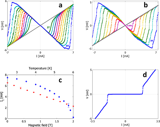
Figure 6. (a) V(I) characteristics at 2 K of a S–I–F junction at various out-of-plane magnetic fields: from the wider to narrower curves, the magnetic field changes from 0 T to 2 T in 0.2 T increments. The linear gray curve was taken at 0 T above TC (10 K). (b) V(I) characteristics of a different S–I–F junction at various temperatures at 0 T. From the wider to narrower curves, the temperatures are: 3, 4, 4.5, 5, 5.25, 5.5, 5.75, 5.85, and 6.25 K. (c) Dependence of  on magnetic field (red circles) and temperature (blue diamonds), extracted from the data in (a) and (b). (d) V(I) characteristics measured at 2 K of a S–F junction (no AlOx
), exhibiting no negative resistance.
on magnetic field (red circles) and temperature (blue diamonds), extracted from the data in (a) and (b). (d) V(I) characteristics measured at 2 K of a S–F junction (no AlOx
), exhibiting no negative resistance.
Download figure:
Standard image High-resolution imageWe now suggest a simple model to explain the transition between negative and positive voltages, attributed to our measurement configuration and pinholes in AlOx
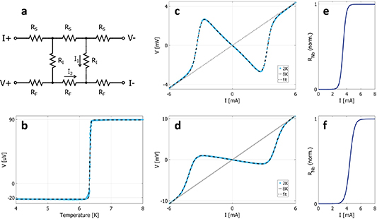
layer, based on a model used by Pomeroy and Grube [13]. The model relies on the passage of current through the insulating layer at distinct local points, each represented as a resistor with resistance  , as illustrated in figure 7(a) (an extended model is described in the supplementary information, figure S11). The S and F layers are represented as resistors with resistances
  and
and  , respectively. The voltage can have two contributions: one from the passage of current between layers (
 in figure 7(a)) and one from the passage of current in the top or bottom layer (
 ). The two contributions are of opposite sign, thus the sign of the resulting voltage depends on the sign of
  . In our system, the local passage points are due to pinholes within the AlOx
layer, which explains why no negative resistance is observed in the S–F devices. We assume a simplified scenario in which
. In our system, the local passage points are due to pinholes within the AlOx
layer, which explains why no negative resistance is observed in the S–F devices. We assume a simplified scenario in which  and
and  are independent of the applied current and let
  change with current as expected of a superconductor. The resulting voltage measured across the junction is then calculated to be
  . For the case of zero resistance in the Nb the voltage will be negative, and for a finite resistance the voltage will be either positive or negative, depending on the values of
  ,
,  , and
, and  . The model predicts that the transition between negative and positive differential resistance will be around the critical current of the Nb, which is in agreement with the data in figures 6 and 3. The fits of the model to V(T) and V(I) curves measured on two different junctions are well matched as shown in figures 7(b)–(d), and the transition behavior of the Nb from superconducting to normal yielded from the fitting parameters (figures 7(e) and (f)) is appropriate, although it does not show an intermediate 'partially superconducting' state as experimentally observed on the superconducting strip (figure 2).
Figure 7. (a) Proposed resistor model for the S-I-F junctions:  ,
,  , and
, and  represent the Nb, AlOx
, and Co/Pt multilayer, respectively. (b) V(T) curve (measured with a constant current of 50 μA) of the same S–I–F junction as in (d). A clear absolute negative resistance is observed below TC. The black dashed curve displays the model equation, calculated using the parameters obtained from fitting V(I) (d). (c) and (d) Current–voltage characteristics of two S–I–F junctions below TC (blue) and above TC (gray) with an applied out-of-plane magnetic field of 1.5 T, fitted to the resistor model. (e) and (f) The transition of Nb from the superconducting to the normal state as obtained from the fitting parameters from the data presented in panels (c) and (d), respectively.
represent the Nb, AlOx
, and Co/Pt multilayer, respectively. (b) V(T) curve (measured with a constant current of 50 μA) of the same S–I–F junction as in (d). A clear absolute negative resistance is observed below TC. The black dashed curve displays the model equation, calculated using the parameters obtained from fitting V(I) (d). (c) and (d) Current–voltage characteristics of two S–I–F junctions below TC (blue) and above TC (gray) with an applied out-of-plane magnetic field of 1.5 T, fitted to the resistor model. (e) and (f) The transition of Nb from the superconducting to the normal state as obtained from the fitting parameters from the data presented in panels (c) and (d), respectively.
Download figure:
Standard image High-resolution image
We note that for the simple (unphysical) case of two passage points (i.e., pinholes), the condition for positive voltages is unlikely ( ) since
  represents the insulating AlOx
layer; however, when extending our model to more than two passage points we obtain negative voltages for
represents the insulating AlOx
layer; however, when extending our model to more than two passage points we obtain negative voltages for  , as expected, and positive voltages for a finite
  , and for
  (see supplementary information, figure S11).
4. Conclusions
Voltage jumps anomalies in the V(I) characteristics measured on the superconducting layer of a S–I–F device can be associated with the interplay between magnetism and superconductivity due to the presence of pinholes in the S–I–F junctions. The pinholes-modulated coupling between the S and F layers accounts for the qualitative hallmarks of the voltage jumps and the related memristor-type behavior. The S–I–F junctions also display an unusual negative to positive resistance transition, which is governed by the critical current in the superconducting layer and its dependence on temperature and magnetic field. A simple circuit model is able to explain the experimental data quantitatively. We note that similar effects (negative resistance, voltage jumps) should be observed for superconductor–insulator-normal metal heterostructures. However, the hysteretic nature of the voltage jumps (with magnetic field) is a result of the ferromagnetic order in the F, as well as the strength of the effect (as the proximity from a ferromagnet is greater). All the aforementioned effects can be associated with the presence of pinholes in the AlOx layer and can be potentially tailored into superconducting-based memory, logic and switching devices.
Acknowledgments
We thank Hen Alpern and Nir Sukenik for helpful discussions and Ofek Vardi for the digital illustration. The research was supported in parts by the Grants from the Academia Sinica—Hebrew University Research Program (O M and Y P). O M thanks support from the Israel Science Foundation Grant Nos. 576/21 and the Harry de Jur Chair in Applied Science. J W A R and M S A acknowledges funding from the EPSRC through the EPSRC-JSPS Core-to-Core Grant (No. EP/P026311/1). M O thanks a scholarship from the Hebrew University Center for Nanoscience and Nanotechnology.
Data availability statement
The data cannot be made publicly available upon publication because no suitable repository exists for hosting data in this field of study. The data that support the findings of this study are available upon reasonable request from the authors.
Supplementary data (3.4 MB DOCX)