

Abstract
The gate-tunable superconductivity in metallic superconductors has recently attracted significant attention due to its rich physics and potential applications in next-generation superconducting electronics. Although the operating principles of these devices have been attributed to the small leakage currents of high-energy electrons in recent experiments, the generated phonons can spread over considerable distances in the substrate, which may limit their further applications. Here, we utilize a top gate structure with monocrystalline h-BN as a gate dielectric and demonstrate the gate-adjustable supercurrent in a metallic Nb microbridge. The gate current of the devices perfectly follows the Fowler–Nordheim law of field emission, indicating that the injection of high-energy electrons presumably causes the suppression of the supercurrent. Our devices reduce the distance between the gate and the microbridge to a few nanometers or less, significantly minimizing the generated phonons' spreading distance and power dissipation in the substrate or surrounding environment. These observations demonstrate that top-gated metallic superconducting switches with local electron injection can improve the device integration density, providing us with more versatile and practical opportunities to explore superconducting circuit architecture.
Export citation and abstract BibTeX RIS
1. Introduction
Tunable superconducting units have provided exciting potential for quantum computing architectures [1–3], fast classical superconducting integrated circuits [4–6], single-photon detectors [7–11], and so on. For instance, by adjusting the parameters of the circuit elements, it is possible to manage the energy level spectrum of superconducting qubits [12, 13], such that their characteristics and operating mechanisms are predictable and controllable in terms of transition frequency and anharmonicity [14–17]. Since the superconducting circuit conventionally consists of flux-controlled superconducting quantum interference devices, the scope of their application is limited by complicated signal coupling and magnetic field-free environments [18–20]. As a result, electrical control of superconductivity would be desirable for integrations and applications of energy-efficient superconducting electronics.
Recent works on gate-controlled metallic nanostructures have received broad interest in the origin of the effect. Giazotto and coworkers first observed a gate-tunable supercurrent in all-metal superconducting nanowires with small leak currents [21]. They attribute the suppression of the critical current to the field effect, combined with the investigations into the gating effects of all-metal suspended nanowires [22], plane Josephson junctions [23], ionic liquid-based nanotransistors [24, 25], and Dayem-bridges [26–29]. The realization of metallic superconducting field-effect transistors would be appealing, but there are also many controversies over these findings due to the current understanding of electrostatic screening in metals. More recently, several more experiments have examined the behaviors in tunnel junctions [30], resonators [31], and designed nanostructures [32–34]. In these experiments, high-energy quasiparticle injection was believed to be responsible for the tunability of the gated metallic nanostructures. Nonetheless, it was also shown that the relaxation of high-energy electrons will generate phonons, which travel through the substrate for a relatively large distance. The non-local nature of the observations in the planar structure may seriously limit the applicability of device integration [35]. Therefore, controlling the metallic superconductivity with limited power spreading would be highly desirable for further developing superconducting electronics.
In this work, we demonstrate the gate-voltage-induced suppression of supercurrent in a metallic Nb microbridge by exploiting a top gate structure with monocrystalline h-BN as a gate dielectric of a few nanometers thickness. The experimental results reveal that the small distance between the gate and microbridge enables minimal power dissipation and local tunability in the devices. Our work elucidates the top-gating effect in metallic superconductors, revealing more obvious advantages over previously reported planar metallic transistors due to the high-energy electron local injection and opening up a new route for developing the superconducting electronics with new functionality.
2. Sample fabrication and measurement techniques
We develop a top gate structure by using h-BN as the dielectric layer to minimize the distance between the gate and the superconductor, which enables the investigation of the gating effect in metallic superconductors on several nanometer scales of gating distance. BN crystal possesses desirable properties for our vertical devices, such as a high-quality insulator with a large bandgap, low dielectric constant, and precise control over thickness at the atomic layer level [36, 37]. Thus, it is an ideal choice for serving as the insulating layer in our devices. An optical image of the device is shown in figure 1(a). We sputtered 10 nm-thick Nb and 2 nm thick Au microbridges on a sapphire substrate by photolithography and a lift-off technique. The length of the central part of the microbridge is 10 μm, and its width is 2 μm. Here, the Au layer prevents the Nb film from oxidizing. Then, we used the PDMS film to stack the h-BN dielectric layer (about 6 nm, see supplementary materials figure S1) onto the Nb bottom microbridge via a dry transfer technique. After this, the other Nb film (about 50 nm thick) was patterned and deposited on the heterostructure to serve as the top gate electrode. Here, we use the Nb superconductor as gate electrodes rather than other conventional metals to avoid affecting the underneath microbridge with resistance-induced Joule heating. Figure 1(b) shows the schematic of our device together with its measurement setup. We measured the current–voltage characteristics (IVCs) of the microbridge by the standard four-probe technique in a Gifford–McMahon refrigerator at different bath temperatures (in the range of 3–7 K). We also recorded the gate voltage and current from the gate electrode to the microbridge.
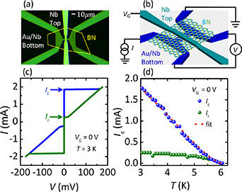
Figure 1. Device layout and basic characteristics. (a) Optical microscope image of the overall structure. The area enclosed by the yellow solid line is the h-BN flake. The overlapping area has a dimension of 2 × 4 μm2, where the bottom microbridge and the top gate electrode have a width of 2 μm and 4 μm, respectively. (b) Schematic of the device. A four-probe setup is used for all the measurements. (c) Current I vs. voltage V characteristics were measured at T = 3.0 K, and VG = 0 V. The critical current Ic and the retrapping current Ir are denoted by the blue and green arrows, respectively. (c) Temperature dependence of the critical current Ic and the retrapping current Ir.
Download figure:
Standard image High-resolution imageFigure 1(c) shows the IVCs of the microbridge at the bath temperature of 3 K. The I–V characteristics show typical hysteretic behavior with a critical current Ic of 1.8 mA and a retrapping current Ir of 0.25 mA at 3 K, which stems from the self-heating effect in the microbridge [38, 39]. With the temperature increasing, the critical current Ic exhibits an apparent decrease. Shown in figure 1(d) is the dependence of both Ic and Ir on the temperature. The Ic vs. T behavior shows a good agreement with Bardeen's equation (red dashed line) [40]: ![${I_{\text{c}}}\left( T \right) = I_{\text{c}}^{\,0}{[ {1 - {{( {\frac{T}{{{T_{\text{c}}}}}})}^2}}]^{\frac{3}{2}}}$](https://content.cld.iop.org/journals/0953-2048/36/9/095005/revision2/sustace65fieqn1.gif) , where the fitting parameter
, where the fitting parameter  = 2.7 mA is the zero-temperature critical current, Tc = 6.05 K is the critical temperature of the superconducting microbridge. The latter value of the critical temperature is consistent with the experimental result determined from the resistance R vs. temperature T curve, as shown in figure 4(b).
To investigate the gating effect on the superconductivity of our device, we measured the IVCs of the microbridge as a function of the voltage applied to the gate electrode. Figure 2(a) shows the IVCs recorded at 3 K for different values of the top gate voltages. The critical current exhibits little change up to |VG| ∼ 1 V. However, it is significantly suppressed at higher |VG|. This observation indicates that applying top gate voltage will lead to the reduction and quenching of critical current, consistent with the previous results [21, 30, 33, 34]. The dependence of the supercurrent on the gate voltage at different temperatures was investigated in detail, as shown in figure 2(b). Similar characteristics of Ic vs. VG for all temperatures are presented, i.e., Ic remains a plateau until |VG| is lower than about the threshold voltage Vth ∼ 0.8 V and decreases to zero at a critical gate voltage VGC ∼ 2.2 V. The asymmetry in the Ic(VG) curves for the positive and negative voltage bias can presumably be explained by the asymmetry of the device, which is discussed in supplementary material figure S6. We note that the values of Vth and VGC display little change with increasing bath temperature, as shown in figure 2(b), indicating that the origin of Ic suppression can be attributed to localized leakage current-induced Joule heating effect [34, 41]. Further analysis regarding this consideration is discussed in supplementary materials figure S3.
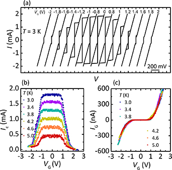
Figure 2. (a) Selected IVCs for device A for several values of gate voltage VG and at a temperature of 3 K. The curves are horizontally offset for clarity. (b) The critical current Ic as a function of the gate voltage VG for different temperatures. (c) The leakage current IG as a function of gate voltage VG for different temperatures.
Download figure:
Standard image High-resolution imageWe now focus on the possible origin of the gate modulation of the supercurrent in the microbridge. The maximum electric field in our experiment is estimated to be up to 370 MVm−1 at the VGC by measuring the thickness of the dielectric h-BN layer, which is consistent with the order of magnitude in other reports [22, 30, 34]. As we know, the high electric field will also induce the field electron emission effect, which results in electron tunneling from the gate electrode into the microbridge [42]. To study the impact of field electron emission on the device, we monitored the gate current IG from the gate electrode to the microbridge while applying the gate voltage VG, as shown in figure 2(c). We found that the variation of the gate current was temperature-independent but strongly related to the gate voltage. The measured IG is negligible until the |VG| reaches the threshold voltage Vth, and when the gate voltage continues to increase, a substantial increase can be observed in the gate current. Such an increase in the gate current, which can be attributed to the field-emitted electrons, might be responsible for the weakening of the supercurrent in the microbridge [31–33].
The above consideration can be better appreciated by the parametric plot of the IG(VG) characteristics shown in figure 3(a). In our case, the supercurrent Ic strongly decreases with the enhancement of the gate current IG and gets fully quenched at about IG ∼ 0.5 μA. Such a behavior resembles previously observed results [34], where the gating mechanism is ascribed to high-energy electron injection. Quantitatively, the field emission-induced gate current IG(VG) behavior can be described by the Fowler–Nordheim equation [43–46]:
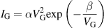
Figure 3. (a) Critical current Ic as a function of gate current IG for several bath temperatures. (b) The IG(VG) characteristic is fitted to the expected Fowler–Nordheim relation for device A. The inset displays the schematics of the relaxation of high-energy electrons by emitting phonons (ph) into the superconductor, causing the quench of the superconductivity.
Download figure:
Standard image High-resolution imagewhere α and β are the parameters relating to the BN dielectric and the device's geometry (see supplementary materials part 2). As expected, we find excellent agreement between the experimental data and the theory shown in figure 3(b). The red line corresponds to the fitting parameter  and
and  (
( ), yielding the barrier height
  0.25 eV (0.30 eV) for positive (negative) bias. The barrier height is smaller than the work function of Nb 4.3 eV [47, 48], which is consistent with previous works [31]. Note that the asymmetry of the IG(VG) characteristics is presumably attributed to the asymmetry of our device. We have provided the energy band diagram of the device in supplementary materials figure S6, illustrating that the potential barrier height for electrons tunneling with a positive voltage bias is lower than that with a negative voltage bias [46, 49]. As a result, the observed asymmetry in IG(VG) shown in figure S6(c) indicates that the gate current is greater for positive bias than for negative bias at the same voltage value.
All the above analyses validate that the field emission electrons play a significant role in the observed critical current modulation in the superconducting microbridge. As reported previously [31–33], those high-energy electrons relax by producing phonons in the BN barriers [32], which will carry sufficient energy to destroy the superconductivity locally depicted in the inset of figure 3(b).
Having demonstrated that the field emission electrons are the leading cause of the Ic suppression, let us now analyze the power generated in the device. The dependence of the Ic on the power PG generated by the applied gate voltage is shown in figure 4(a), where we obtain PG = VG
IG. An indication that the injection heat power produced by the gate should not be excluded is evident in the sharp fall of the Ic value for the slight enhancement of the gate power PG [33]. To investigate the leakage current-induced heat power in the device, we have studied the relationship between the effective electronic temperature (Te) and the gate power (PG). To determine the value of Te, we compared the Ic(PG) characteristic with the temperature calibration curve, Ic vs. T, presented in figure 1(d). The gate power relaxation of the electrons in the bottom Nb film can be described as  where Te represents the electronic temperature, TL represents the lattice temperature, A represents the contact area, and
  is a constant dependent on the interface material [50]. We have plotted
  as a function of PG in the modified figure 4(b) and have observed a linear dependence for various bath temperatures. The linear approximation exhibits good agreement with the experimental data when using a k value of 66.5 Wm−2K−4, which is of the same order as in previous studies in Cu, graphene and NbN films [51–53]. Hence, we propose that the origin of the observed critical current suppression could presumably be attributed to the leakage current-induced gate power (PG) relaxation in the bottom Nb microbridges by the electron–phonon interaction [50, 51], as depicted in supplementary materials figure S4.

Figure 4. (a) The critical current Ic as a function of gate power PG for several bath temperatures T. (b)  as a function of the gate power PG for different bath temperatures T. A linear dependence (red dashed line) is observed for all temperatures. (c) Resistance R as a function of temperature T for several gate voltages with a bias current of 20 μA. The cyan arrow indicates the onset temperature Tc1 of the microbridge, and the red arrow means the offset temperature Tc2 where the resistance reaches zero. (d) The extracted Tc1 and Tc2 vs. gate voltage VG, where the inset shows the schematic of the characteristics of the microbridge under gating. The R1 and R2, denoted by the black arrows shown in figure (b), represent the resistance of the whole microbridge and the gating area.
Download figure:
Standard image High-resolution image
We recorded the temperature (T) dependence of the resistance (R) as a function of the applied gate voltages with a dc bias current of 20 μA, as shown in figure 4(c), to analyze the injection power distribution along the superconducting microbridge. Furthermore, we have noted that the oscillation amplitude of the resistance at VG = 2 V is the same as the amplitude at zero resistance. Based on these findings, we speculate that the oscillations in resistance could be caused by environmental noise. It is known that any thermal injection can suppress the critical current, resulting in a reduction in the critical temperature [54]. We observed that each of the R vs. T curves with gating in figure 4(c) has two transition temperatures, Tc1 and Tc2, denoted by the cyan arrow and the red arrow, respectively. The oscillation in the R–T curves with gate voltages can be attributed to the environmental noise, in which the oscillation amplitude is consistent with oscillation amplitude observed at zero resistance. In addition, the R–T curves under different gate voltages show two intersection points, i.e. R1 and R2 as shown in figure 4(c). The value of Tc1 remains substantially constant within an experimental error as the gate voltage increases, while the value of Tc2 decreases gradually with the increasing gate voltage, shown in figure 4(c). The observation indicates that the gate voltage partly weakens the strength of the superconductivity in the microbridge.
From the R(T) characteristics, we can also quantitatively infer the gating distribution in the microbridge. As illustrated in the inset of figure 4(d), the onset of Tc1 and Tc2 has resistances of R1 ∼ 86.5 Ω and R2 ∼ 36.2 Ω, corresponding to the resistance of the whole microbridge and the gating area, respectively. Noticeably, the ratio of the resistances is roughly 2.4, which is comparable with the ratio of 2.5 of the microbridge length to the gating width. In this scenario, the high-energy quasiparticles generated could reach the superconducting bridge via the nanoscale BN layer, which would prevent phonons from dissipating outside of the gate channel, leading to the local tunability of the supercurrent in the microbridge.
3. Discussion
Finally, we remark on the potential advantages of our devices with top gate structures. To our knowledge, the retrapping current Ir reflects the minimum current level of the normal state of the microbridge [39, 55]. Therefore, the minimum power to quench the superconductivity of the whole microbridge is given as Pr = Ic 2 RN, which relates to the retrapping current Ir and normal state resistance RN of the microbridge. For device A, the Pr ∼ 5.5 μW is derived, where Ir ∼ 0.25 mA, and RN ∼ 88 Ω. However, the gate-induced power PG ∼ 1 μW at the supercurrent quenching point is obtained from figure 4(a), which is several times smaller than the Pr value. This is strikingly in contrast to previous works demonstrated in superconducting nanowires with planar geometry [26, 27, 30, 33], in which the gate power is found to be considerably larger than the power of Pr. Here, we attribute this phenomenon to the nano-scaled separation of the superconductors from the gate.
As discussed above, the gate current dependence on the gate voltage is consistent with the behavior of high-energy electron emission by the strong electric field. In this case, the electrons relax by generating phonons that reach the superconducting Nb microbridge by traveling through the thin BN dielectric layer [30]. We note here that the gate distance is limited to a few nanometers, so the generated phonons propagation scope is strongly confined in our device compared with the previous planar structure [28, 29, 31, 33, 34]. As a result, the small phonons propagation distance could account for the difference between Pr and PG, that is, the local quasiparticle injection only affects the gating area, not the superconductivity of the whole bridge.
In addition, we should also consider the thermal relaxation when the phonons arrive in the Nb superconductors microbridge. First, as the gate current (below 1 μA) is much lower than the critical current of the top superconductor (about several hundred μA), the power dissipation of the top gate electrode in the substrate or surrounding environment can be ignored. Second, the applied gate voltage did not result in any observable change in the onset critical temperature Tc1 (figure 4(b)), indicating that the top-gating in our device might be a local phenomenon. Due to the lower rates of phonon–phonon scattering, it should be noted that the phonon generation in the system may be more effective than for low-energy electrons injection [56, 57]. We expected that the nanoscale gate distance and efficient relaxation of phonons would be highly desirable for the integration and application of the devices.
In summary, we have demonstrated the top gate-controlled superconductivity in the Nb microbridges by using the h-BN dielectric layer. Our results suggest that the supercurrent suppression with gating could be attributed to the field emission electrons generated between the gate electrode and the microbridge by the strong electric field. By investigating the transport characteristics of the microbridges with gate voltages, we have observed that only the superconductivity in the gated region is suppressed. The possible origin of this behavior may be that the power spreading in the device is minimized due to the nanoscale distance between the gate and the microbridge, in contrast to previous work with in-plane nanostructures. The devices exhibit clear advantages for potential applications in superconducting quantum architectures and logic circuits, which would benefit from its top gate structure to improve device integration density and energy efficiency.
Acknowledgments
We gratefully acknowledge financial support from the National Key R&D Program of China (Grant Nos. 2021YFA0718802, 2018YFA0209002), the National Natural Science Foundation of China (Grant Nos. 62288101, 61727805, 11961141002, 62201005, 62201396, 62101243, 62274086), and Jiangsu Key Laboratory of Advanced Techniques for Manipulating Electromagnetic Waves.
Data availability statement
The data that support the findings of this study are available upon reasonable request from the authors.
Supplementary data (0.5 MB PDF)