
Abstract
This article discusses key elementary surface-reaction processes in state-of-the-art plasma etching and deposition relevant to nanoelectronic device fabrication and presents a concise guide to the forefront of research on plasma-enhanced atomic layer etching (PE-ALE) and plasma-enhanced atomic layer deposition (PE-ALD). As the critical dimensions of semiconductor devices approach the atomic scale, atomic-level precision is required in plasma processing. The development of advanced plasma processes with such accuracy necessitates an in-depth understanding of the surface reaction mechanisms. With this in mind, we first review the basics of reactive ion etching (RIE) and high-aspect-ratio (HAR) etching and we elaborate on the methods of PE-ALE and PE-ALD as surface-controlled processing, as opposed to the conventional flux-controlled processing such as RIE and chemical vapor deposition (CVD). Second, we discuss the surface reaction mechanisms of PE-ALE and PE-ALD and the roles played by incident ions and radicals in their reactions. More specifically, we discuss the role of transport of ions and radicals, including their surface reaction probabilities and ion-energy-dependent threshold effects in processing over HAR features such as deep holes and trenches.
Export citation and abstract BibTeX RIS

Original content from this work may be used under the terms of the Creative Commons Attribution 4.0 licence. Any further distribution of this work must maintain attribution to the author(s) and the title of the work, journal citation and DOI.
1. Introduction
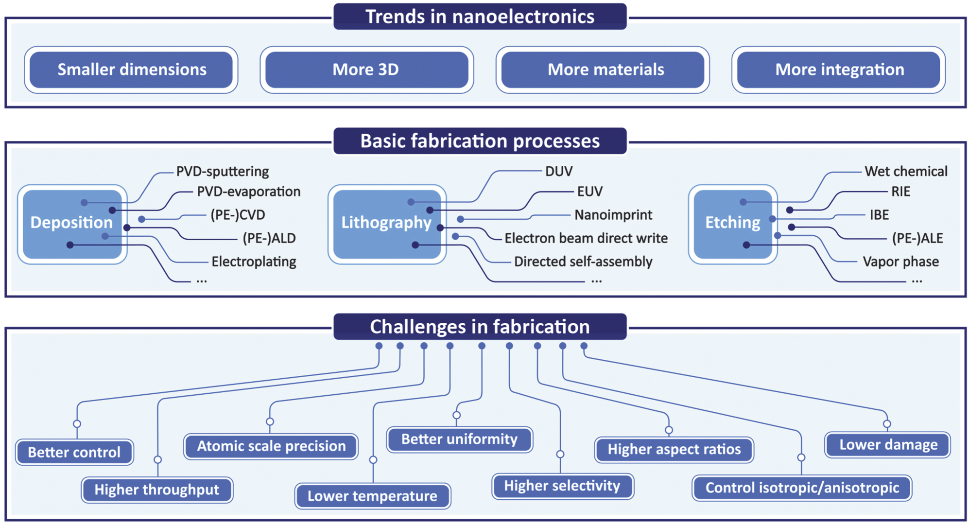
Four key trends can be observed for state-of-the-art semiconductor devices: (i) the critical dimensions in the devices are approaching the atomic scale, (ii) more devices are becoming three-dimensional (3D), (iii) the devices involve increasingly unconventional materials, and (iv) the fabrication requires higher integration complexity. The deposition, lithography, and etching techniques to fabricate such devices are facing extreme challenges as summarized in figure 1. For example, etched features are becoming narrower and deeper, and deposited films are becoming thinner and need to be more conformal over complex 3D surface topographies [1–3]. Low-temperature (i.e., near-room-temperature) processing is often desired because of the growing presence of temperature-sensitive materials. Precise and uniform control over fabricated features is needed in such nanoscale processes and can be achieved by improving the process selectivity over different materials and topographies as well as the control of the etch rates, thicknesses of deposited films, and process-induced damages.

Figure 1. Trends and challenges in the fabrication of present-day nanoelectronics. Various established techniques for deposition, lithography, and etching are indicated. [PVD: physical vapor deposition, (PE-)CVD: (plasma-enhanced) chemical vapor deposition, (PE-)ALD: (plasma-enhanced) atomic layer deposition, DUV: deep ultraviolet lithography, EUV: extreme ultraviolet lithography, RIE: reactive ion etching; IBE: ion beam etching, and (PE-)ALE: (plasma-enhanced) atomic layer etching.]
Download figure:
Standard image High-resolution imagePlasmas can provide a wide range of controllability for deposition and etching techniques [4–9]. The fact that a plasma is in non-thermal equilibrium allows it to be a source of highly reactive species (e.g., radicals) and energetic ions at low gas temperature. Indeed most anisotropic etching processes [6, 10–12] and many deposition processes [13–17] are plasma-based, being enabled by the directional ion bombardment and high reactivities of radicals generated in plasmas.
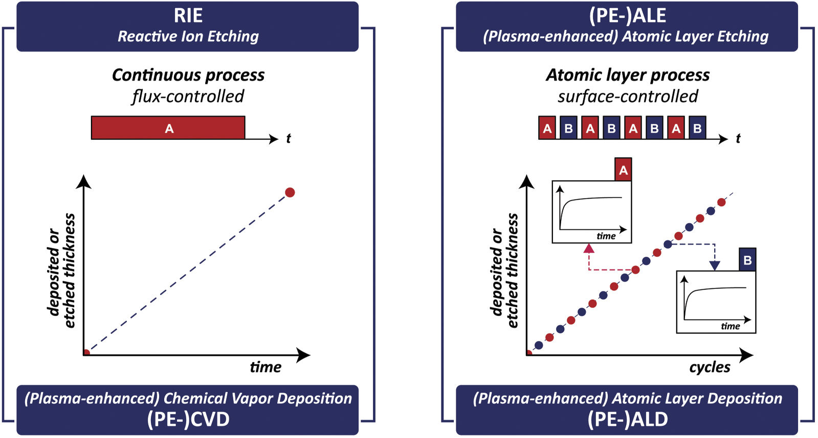
Examples of well-established ion and plasma processing techniques include RIE, ion beam etching (IBE), plasma-enhanced chemical vapor deposition (PE-CVD), and physical vapor deposition (PVD). A common factor of these techniques is that the amount of etched or deposited material scales with the total dose of energetic ions and/or reactant species. While such flux- or dose-controlled techniques continue to have important applications, surface-controlled processing techniques, which are less dependent on the total dose of incident ions or reactant species, are now playing increasingly important roles in various areas, including semiconductor device fabrication. The surface-controlled processing techniques include atomic layer etching (ALE) [15, 18–22] and atomic layer deposition (ALD) [13, 17, 23, 24]. Plasmas are often used in ALD and ALE, in which case the techniques are referred to as plasma-enhanced atomic layer etching (PE-ALE) and plasma-enhanced atomic layer deposition (PE-ALD). These processes may be collectively called atomic level, atomic layer or atomic-scale processes. In any case, ALD and ALE are repetitive processes where an atomic layer of a material is removed or added in each cycle and this cycle is repeated a number of times to etch or deposit a targeted amount of the material.
The distinction between continuous and atomic layer processes is illustrated in figure 2, which shows the etched or deposited film thickness as a function of the process time or the number of process cycles for a continuous process (RIE or CVD) or a surface-controlled process (ALE or ALD). In a continuous process, the deposited or etched film thickness typically scales with the process time while, in a surface-controlled process, deposited or etched film thickness scales with the number of cycles. In the latter, A and B denote the first and second half-cycles. In this example, the insets show that the amounts of deposited or etched materials saturate in time, i.e., both half-cycles are self-limiting.

Figure 2. Etched and deposited film thickness as a function of the process time for a continuous process (e.g., RIE or CVD) or the number of process cycles for a surface-controlled process (e.g. ALE or ALD). In a continuous process, the etched or deposited film thickness is typically proportional to the process time while, in an atomic layer process, the etched or deposited film thickness is proportional to the number of cycles. In the latter, A and B denote the two half-cycles.
Download figure:
Standard image High-resolution imageA generic representation of a single cycle of an atomic layer process is schematically depicted in figure 3, where each circle represents an atom or reactant species and each frame represents a cross-section of the surface. A single cycle typically consists of two half-cycles: in the first half-cycle, the surface is modified by incident reactant species. In the second half-cycle, this modified layer is exposed to other reactant species and/or energy and gets activated, so that the modified layer either desorbs (ALE) or becomes converted to the material of the growing film, adding a monolayer to it (ALD). For ALE, this activation half-cycle is often called the desorption step. The first and second half-cycles are separated in time and a purge step may be employed after each half-cycle.
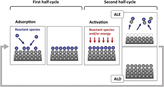
Figure 3. A cycle of an atomic layer process such as ALE and ALD typically consists of half-cycles: in the first half-cycle, the surface is modified by the adsorption of incident reactant species (adsorption step). In the second half-cycle, this modified surface is exposed to different reactant species and/or energy and gets activated (activation step). In ALE, the modified layer containing the surface atoms desorb in the activation step. In ALD, the modified layer is activated and converted to the material of the growing film, thus adding a monolayer to it in the activation step. Each half-cycle takes place in a self-limiting manner. The cycles are repeated a number of times to etch or deposit the targeted amount of material.
Download figure:
Standard image High-resolution imageIn the strict sense, the surface reactions in each half-cycle take place only at the very top surface monolayer. Furthermore, the reactions are self-limiting in the sense that they terminate after some time. For example, the surface modification of the first half-cycle stops after all available surface reaction sites are saturated with adsorbed species, and the surface activation in the second half-cycle stops after the modified layer either desorbs (ALE) or gets converted to the surface material (ALD). This makes the processes surface-controlled, as opposed to flux-controlled. It is important to keep in mind that real atomic layer processes may not be as ideal as defined here. For example, some processes show cycles with 'soft-saturation'. This means that adsorption or desorption of surface species slows down but does not stop completely at prolonged exposures. In other real-life cases, one of the half-cycles may not be self-limiting at all. It is also possible that the reactions occur in a surface layer with a thickness of the order of a nanometer, rather than only the top monolayer.
The self-limiting character (at least in one of the half-cycles) is an essential aspect of ALE and ALD processes. It is important in the following two ways: first, because each cycle is known to process a limited amount of the surface layer, we can ensure accurate control of etched depth or deposited film thickness by selecting the number of cycles in the process. Second, one can also ensure that the process can take place uniformly over a large area, regardless of the local density of complex surface structures. For example, under the continuous process, the etching or deposition rate at the bottom of a narrow trench is typically lower than that at the bottom of a wide trench because the flux of gaseous species reaching the bottom is lower in the narrow trench. On the other hand, in ALD and ALE, the etching or deposition of a monolayer at the bottom of a wide trench may terminate earlier than that at the bottom of a narrow trench. However, the etching or deposition is completed eventually in both structures by the time the saturation conditions are satisfied for every surface within the structures. By repeating this cycle many times, one can achieve a highly uniform process over a wide area of complex structures. These advantages of the surface-controlled processes over the flux-controlled processes are illustrated for ALD in figure 4. A disadvantage of atomic layer processes is that it typically takes a much longer time to etch or deposit a desired amount of material than the corresponding continuous process. Throughput during ALE and ALD is, therefore, an important topic in equipment design and process development in the industry. In academic studies, typically long dose- and purge steps of a few seconds are used, such that one cycle can take tens of seconds and even up to a minute in more extreme cases. However, this is usually done to study pure ALE and ALD processes, with complete saturation and without any overlap between the two half-cycles. In industry, equipment and processes are optimized for particular chemistries and applications and cycle times can go sub-second. Moreover, the cycle time will be made as short as allowed by the application dropping the need for true ALD or ALE behavior [15]. Despite the disadvantage of lower throughput, there is an increasing demand for surface-controlled techniques, as is reflected, for instance, in the global market size of ALD, which has increased by over 300% since 2010 [1, 25].

Figure 4. Merits of a surface-controlled process—as illustrated for film growth by ALD—in comparison to a flux-controlled processes (e.g., film growth by CVD and PVD). In the surface-controlled growth process, the amount of deposited material is independent of the local flux of reactant species supplied by the source, which leads to excellent uniformity, conformality, and thickness control. The bottom part of the figure shows the conditions with a low and high flux. For ALE a similar situation holds as for ALD. Reprinted from [14], Copyright (2014), with permission from Elsevier.
Download figure:
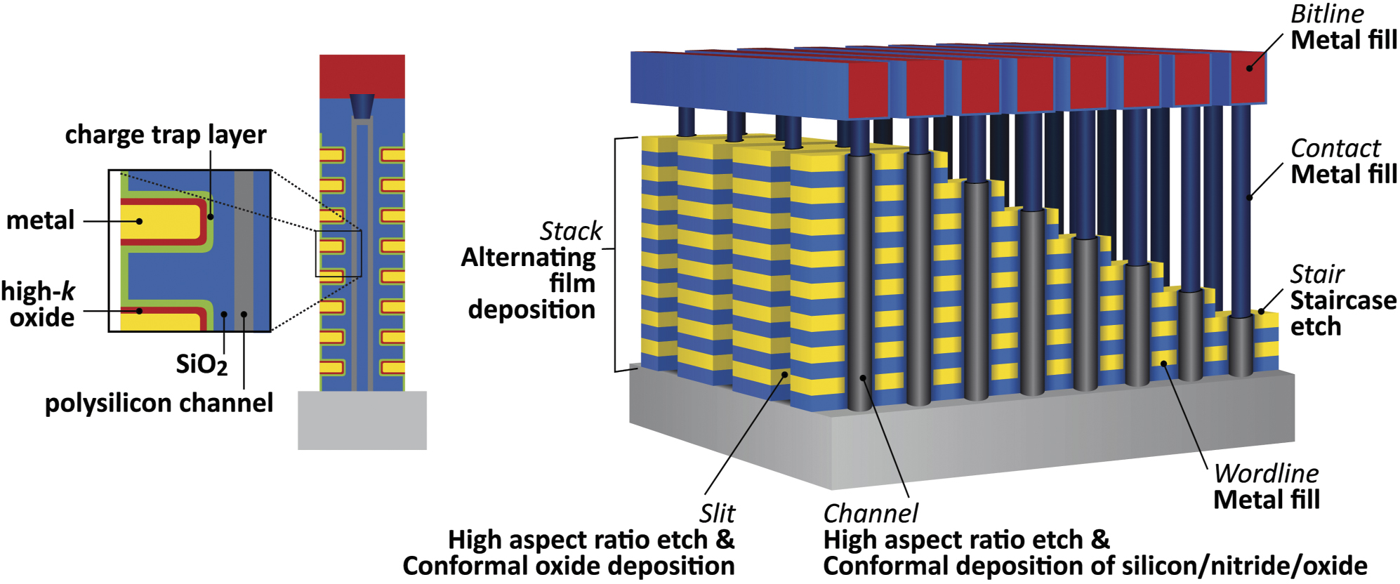
Standard image High-resolution imageThe latest trends in nanoscale processing and the growing need for more precisely controlled plasma processing are well exemplified in the fabrication of 3D NAND devices. NAND is a non-volatile memory (also referred to as flash memory) based on not-AND logic gates used in memory sticks, memory cards, and solid-state drives. A typical structure of a 3D NAND device is illustrated in figure 5, where the processing techniques to form specific parts of the device are also indicated (see, for instance, Kim et al [26] for further details). More than a decade ago, two-dimensional NAND devices were approaching their scaling limit due to the increased cell-to-cell interference [26]. To overcome this scaling limit, the 3D NAND architecture was introduced, where the areal density of bit lines was increased by the multiple word line stacking in the vertical direction [26]. Since the mass production of 3D NAND devices started in 2013, the number of word line layers has increased by 30%–50% for each generation [26], up to 232 layers for the present-day devices involving double-stack technology [27, 28]. The increased aspect ratio (AR), i.e., the ratio of the depth of the structure to its typical lateral size (depth/diameter in the case of a vertical hole or the depth/width in the case of a slit or trench), is now exceeding 40 for a single-stack etch process, make the etching highly challenging. This is firstly because fewer reactant species needed for efficient RIE reach the bottom of a higher AR structure, and secondly because mechanical stress generated in such etching processes can collapse fragile structures. Thin-film deposition over the inner walls of such deep structures is another technological challenge. To address this challenge, ALD is being used. For example, PE-ALD is employed for conformal deposition of silicon dioxide (SiO2) liners on the vertical slits [1].

Figure 5. Schematic illustration of a 3D NAND memory device and the processes used to fabricate specific structures of the device. The figure shows the case for a single-stack whereas double-stack technology is now state-of-the-art (based on a figure published by Lam Research Corp. [30]).
Download figure:
Standard image High-resolution imageIn the fabrication of advanced logic and memory devices with plasma-based deposition and etching processes, it can be very demanding to achieve suitable plasma conditions, such as the right energy and flux of ions and radicals. The process tool equipped with plasma sources, therefore, plays an important role. The types of plasma systems used for PE-ALE and PE-ALD are typically quite similar to those used in RIE and PECVD [5], mostly being capacitively coupled plasma (CCP) and inductively-coupled plasma (ICP) systems but with hardware changes to allow for quickly alternating between reactants, optimized purging, and heating of reactor walls, gas, and reactant lines, etc [11, 17, 29]. Multifrequency operation and external substrate biasing are also employed to independently allow for adjusting the plasma chemistry and the incident ion energy. For PE-ALD, CCPs are most popular in the industry, mainly due to their scalability. This also includes high-productivity multi-wafer reactor chambers involving either temporal or spatial ALD. Remote plasma sources such as ICPs and hollow-cathode plasmas are often used in academia due to their enhanced freedom in operating conditions. The use of microwave plasmas, electron-cyclotron-resonance plasmas, and helicon plasmas appear to be rather limited [11, 17].
In this article, we review plasma-based processes used to fabricate nanostructures on material surfaces. Starting from RIE and high-aspect-ratio (HAR) etching, we especially focus on key elementary surface-reaction processes governing PE-ALE and PE-ALD as increasingly used in the semiconductor/nanoelectronics industry. The emphasis is placed on the latest trends and challenges of the processing techniques, highlighting new developments in this field from a plasma–surface interaction perspective. We by no means attempt to provide an exhaustive review of all plasma-based processing techniques that are important in nanoelectronics processes, nor do we extensively cover the plasma sources and plasma physics involved. The article is organized as follows: in section 2, plasma etching techniques used for nanoscale scale electronics are reviewed with a focus on PE-ALE, following a brief discussion on conventional RIE which remains the most widely used etch technology. In section 3, plasma deposition techniques used for nanoscale electronics are discussed with an emphasis on the roles played by radicals and ions for fundamental surface reactions in PE-ALD. The conclusions and future perspectives of plasma-based atomic layer processes are presented in section 4.
2. Plasma etching for nanoscale electronics
2.1. Basics of reactive ion etching
RIE is an etching process combining surface chemical reactions with the energy and momentum transfer from incident ions. In plasma etching, reactant species causing the surface reactions are typically radicals and reactive ions generated in the plasma. The etch rate, i.e., the etched depth per unit time, is much higher in RIE than that by the corresponding thermal chemical reactions or by the corresponding physical sputtering. This is called a synergetic effect, which was epitomized in the pioneering beam study by Coburn and Winters [31]. Because the energy needed to trigger surface chemical reactions is provided by the kinetic energy of incident ions, RIE is intrinsically a non-thermal-equilibrium process and can take place without high surface temperatures. This is one of the main advantages of RIE in semiconductor manufacturing as one can perform etching processes without thermal damage to the prefabricated device structures on the wafer. Another key advantage is what is called anisotropic or directional etching, where etching takes place predominantly in the direction of the ion incidence and allows the fabrication of deep structures.
The etch rates of RIE vary widely, depending on the materials to be etched and the conditions of the incident ions. For ion-induced etching such as RIE, the sputtering yield, i.e. the average number of atoms removed from the surface per ion impact, is an important parameter. Since the sputtering yield is essentially independent of the ion flux, it is a physical parameter intrinsic to the material, in contrast to the etch rate, which does depend on the ion flux. Well-defined ion beam experiments can uncover the elementary surface reactions in RIE processes [32]. For example, detailed beam studies were performed to determine the sputtering yields of Si by Ar+ and Cl+ ions [33–39] and chlorinated Si surfaces by Ar+ [40, 41] for a wide range of ion incident energies. Other beam studies on Si- and C-based materials were also reported [32, 42–47]. In addition [48, 49], ion beam studies were used to determine the sputtering yields of metals [50–61] and metal oxides [60–65]. Binary-collision-model [66–69] and molecular dynamics (MD) [70–72] simulations were also used to study etching and sputtering phenomena theoretically. The results of such simulations are found to be in good agreement with the experimental observations in many cases.
The sputtering yields for many single element materials by single element ions obtained from experiments and binary-collision-model simulations by the mid-90s have been summarized [38]. Based on these data, an empirical formula of the sputtering yield as a function of the ion incident energy was derived by Yamamura and Tawara [38]. A more recent study has shown that the sputtering yield depends strongly on a relatively small number of physical parameters such as the atomic masses of the surface material and incident ions [73]. Taking advantage of such characteristics of sputtering and using machine learning, one can predict unknown sputtering yields based on the existing sputtering yield data for similar materials and incident ion species [74].
The aforementioned studies have also revealed that, the higher the ion incident energy is, the more physical, rather than chemical, the etching process becomes. This is because the collision cascade in the material dominates the sputter phenomena rather than surface chemical reactions when the incident ion energy is high. In RIE, the surface chemical reactions modify a thin layer of the material surface and convert it to a mixed layer consisting of surface atoms and adsorbed chemical species [75]. The mixed layer is typically made of a weakly bonded material and can be etched spontaneously (i.e., sublimated thermally) or sputtered by ion-induced collision cascades more easily than the original material. When the ion incident energy is high, the majority of sputtered species are single atoms or small clusters of atoms (radicals), rather than volatile molecules [76]. Therefore, such desorbed/sputtered species have dangling bonds and are highly reactive when they reach the sidewalls. For example, in a RIE process of Si by chlorine (Cl2)-based plasmas containing a small amount of oxygen (O2), sputtered species such as SiClx from the bottom of the features react with gaseous O radicals on the sidewalls and form thin SiO2 layers, which prevent etching of the sidewalls by Cl radicals. Such layers are called sidewall passivation layers and can play an essential role in achieving anisotropic etching [77–81].
Surface damage caused by energetic ion impact during RIE processes can alter the mechanical and electrical properties of the etched material surface [82, 83]. One of the well-known examples is Si recess [84–86], i.e., the formation of hollow Si profiles around the polycrystalline silicon (poly-Si) gates in the gate etching process. In these processes, poly-Si gate etching was typically performed with hydrogen-bromide (HBr) plasmas containing O2 and the unmasked poly-Si was etched until the gate oxide layer was exposed. Then significant oxidation of Si was found to occur underneath the gate oxide layer. The oxidized Si layer together with the gate oxide was removed in the subsequent oxide removal process by hydrogen fluoride, which resulted in a recess of the etched surface. The Si oxidation is caused by the enhanced diffusion of O atoms of the gate oxide layer to the Si layer by collisions with incident energetic H ions penetrating through the gate oxide layer [87].
Because of the small atomic radius and small mass, energetic H ions can penetrate deeply into a material and be scattered with large scattering angles when they collide with heavy atoms of the material. For nanoelectronics devices, the depth of the damaged layer formed in a RIE process can be comparable to the device size. Therefore, the detrimental effects of H-containing plasmas should not be underestimated. For example, energetic H ions hitting sidewalls with grazing angles can be scattered with large scattering angles and may penetrate into the sidewall materials, damaging the crystalline structure [45, 88].
2.2. High-aspect-ratio (HAR) etching
After discussing the general characteristics of RIE above, we now focus on RIE for HAR structures. As shown in figure 5, HAR structures are widely used in 3D NAND devices. In these devices, structures with an AR up to 40 to 60 [1] are common. To hold a large number of memory cells per chip area, the number of layers (as seen in figure 5) is continuously increasing in every device generation and has now reached 232 for some commercial products [27, 28]. The AR of required HAR contact (HARC) holes can be larger than 100. Creating a HARC with an AR of 100 or higher in a single etch process is still extremely challenging and therefore the double-stack technology is typically employed, in which two stacks of layers with lower-AR contact holes are overlayed (to be in the range of AR 40 to 60). However, to reduce the cost of manufacturing with double-stack processes, single-stack-etch processes aiming at HAR etch with an AR larger than 100 are now being developed.
Some of the main difficulties of HAR etch processes for 3D NAND devices include the slowdown of the etch rates as the etched depth increase (i.e., AR-dependent etch or ARDE) [89–91] and the formation of abnormal hole cross-sections as well as non-straight vertical structures (i.e., bending, bowing, and twisting) [90]. The sidewalls of HARCs can also form ripple-like structures during the etching process, which is known as striation [92]. Such anomalies are typically caused by the ion–surface interactions in the RIE processes, including surface charging effects at the bottom of HAR features that possibly alter the incident ion paths [93]. The effect of surface charging is well studied and concepts have been developed to compensate for this effect [94–97]. However, detailed mechanisms are still not known yet for some of the aforementioned phenomena.
Typical 3D NAND devices consist of stacks of poly-Si/SiO2 [98, 99] or silicon nitride (SiN)/SiO2 [27, 100, 101] pairs. Each layer is typically several ∼10 nm thick. In what follows, we shall only consider HAR etching of SiO2 single-material layer for the sake of simplicity and illustrate the roles that radicals and ions play in HAR etching processes. For RIE etching of SiO2, fluorocarbon (FC) plasmas are typically used with the expectation that the etching process leads to the formation of volatile species such as SiF4, CO, and CO2. In the case of plasma-based HAR etching, although the plasma generates a large number of charge-neutral radicals, they are unlikely to reach the bottom of a HAR structure. This is because charge-neutral radicals in a plasma have large angular distributions in the velocity space (figure 6(a)) and significant surface reaction probabilities, so that, if they enter a deep hole or trench, they tend to get lost by colliding with sidewalls before reaching the bottom. On the other hand, the ion fluxes from the plasma can take many C and F atoms to the bottom in the form of Cx Fy +. The etching process at the bottom is, therefore, caused essentially by such energetic ions only, not by radicals (figure 6(b)).
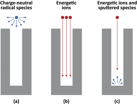
Figure 6. Schematic illustration of transport of radicals (a), ions (b), and sputtered species due to an ion exposure.
Download figure:
Standard image High-resolution imageAt the bottom of a HAR structure, the majority of sputtered species are single atoms or small fractions of molecules, rather than larger volatile molecules, when the incident ion energy is high [76]. These sputtered species tend to react at the sidewalls (especially near the bottom) and contribute to the formation of a deposition layer on the sidewalls (figure 6(c)). If the incident ion energy is sufficiently high, the incident ions hitting the sidewalls with grazing angles can scrape off such newly depositing layers and bring them back to the bottom. In this way, in the case of SiO2 HAR etching by FC plasmas, C and F atoms can accumulate at the bottom, forming a mixing layer consisting of C, F, Si, and O atoms there. This is similar to the mixing layer formation on a flat SiO2 surface exposed to an FC plasma, but the accumulation of C and F on the flat surface is mostly due to the adsorption of radicals generated in the plasma. The fact that the etching proceeds even at the bottom of a HAR structure suggests that Si and O atoms removed from the bottom surface by RIE eventually form volatile species such as CO, CO2, and SiF4 in the mixing layer. Such volatile species are much less reactive than radicals and can leave the narrow and deep HAR structure without reacting on the sidewalls. The transport of radicals and ions in a HAR structure plays important roles in the etching, sidewall film deposition [102–105], and removal of etched products. Such transport plays similarly important roles in the formation of conformal thin films on the sidewalls of HAR structures by ALD, as will be discussed in section 3.2.
At the end of an etching process, it may be required to minimize the damage on the etched surface or to stop the etch process at a specific depth precisely. To meet the requirement, one can switch the RIE process to an ALE process right before the desired depth and profiles are obtained. One such example is (although it is not a HAR etching) a self-aligned contact (SAC) process, which will be discussed in the following subsection.
2.3. PE-ALE: new opportunities by surface-controlled reactions
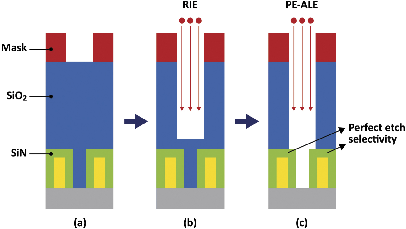
In the remainder of this section, we discuss PE-ALE. One of the well-known applications of PE-ALE in semiconductor manufacturing is an etching process to form SAC holes [21, 106]. Figure 7 shows a SAC etch process schematically. In this process, a deep hole through the SiO2 layer is created, reaching the bottom layer without eroding the silicon nitride (SiN) layers that protect their internal conductors (i.e., gates). The etched hole is to be filled with metal and the SiN layers prevent short-circuiting of the gates with the metal conductor. Such a SAC hole is formed with a mask with a circular opening and FC-based RIE at relatively high ion incident energy (figure 7(a)). The energetic ions could erode the SiN layers, so the RIE process is stopped before the etched front reaches the SiN layers (figure 7(b)), and then the process is switched to PE-ALE, which allows high selectivity of SiO2 etch over SiN (figure 7(c)). Because of the self-limiting and selective chemistry of the SiO2 PE-ALE, once a SiO2 monolayer or thin layer is removed, the etch process stops and does not etch the underlying or adjacent SiN. The ion energies used in the desorption step of typical ALE processes are much lower than those of typical RIE processes. In this way, the erosion of the SiN layers can be avoided.

Figure 7. Schematics diagram of a SAC process. Each picture represents a cross-section of a structure extending into and out of the page. A mask (marked in red) with a circular opening is formed on the SiO2 surface (a) to fabricate a hole through SiO2 that reaches the bottom layer (gray) by plasma etching. In this process, the SiN structure (green) should be kept intact, so that the hole must become narrower between the two SiN structures (c). The etched hole is to be filled with a conducting material and the SiN structures protect their internal conductors from short-circuiting with the vertical hole conductor. To form such a hole, one may first use fast RIE of SiO2 to form a hole and then, right before the RIE-based etch front hits the SiN structures (b), switch to a highly selective PE-ALE of SiO2 over SiN (c) [21, 106].
Download figure:
Standard image High-resolution imageThere are two types of PE-ALE. If energetic ion impact plays an essential role in PE-ALE, it is called ion-driven or anisotropic PE-ALE. Otherwise, plasma-generated radicals cause surface reactions that result in radical-driven, isotropic PE-ALE. In typical anisotropic PE-ALE, the second half-cycle employs ion irradiation without chemical reactions, such as Ar+ ion irradiation. The ion energy is typically kept low to minimize physical sputtering and surface damage. In the SAC etch process examples discussed above, anisotropic PE-ALE for SiO2 was used.
Anisotropic PE-ALE may be considered as RIE with separate surface-reaction and ion-impact steps. In the first half-cycle, adsorbed species modify the surface. In the second half-cycle, the modified surface layer is removed by ion impact. Because the removed layer is the modified layer formed in the first half-cycle, the etched depth per cycle (EPC) should not depend on the ion incident energy in the window with ALE conditions.
The energy dependence of the EPC is schematically depicted in figure 8 for ideal PE-ALE with a sufficiently long duration of the desorption step in the second half-cycle. A modified layer with a thickness of d is assumed to be formed in the adsorption step of the first half-cycle. The modified layer is more readily etched than the original material, so the etch rate of the modified layer is higher than that of the underlying (original) material. If the ion incident energy E is lower than point A, we assume the etch rates for both modified layer and underlying material are zero. Point C represents the sputtering threshold energy of the underlying material. In the energy range between A and B, the etch rate of the modified layer is nonzero and an increasing function of the ion incident energy E whereas the etch rate of the underlying material is zero. For the ion incident energy lower than the sputtering threshold energy of the underlying material, once the modified layer with a thickness of d is completely removed by the ion impact, the etching no longer occurs. This corresponds to the energy range between B and C in figure 8(a), which is called the ALE window [107–109]. It should be noted, by definition, that the higher end of the ALE window corresponds to the sputtering threshold energy. If the ion incident energy is higher than this sputtering threshold energy, physical sputtering of the original material takes place.
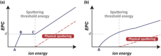
Figure 8. Schematic diagrams of the EPC of an anisotropic PE-ALE process as a function of the ion incident energy of the desorption step of the second half-cycle, represented by the black curves. Point A represents the etching threshold energy of the modified surface layer formed in the adsorption half-cycle. The depth of a modified layer is denoted by d. The red dot-dash line represents the etched amount (depth) by physical sputtering of the surface material in the absence of the adsorption step and the vertical broken line indicates the position of the sputtering threshold energy. Point B indicates the ion energy for which the ion dose in the desorption half-cycle is sufficient to remove the modified layer. The energy range where the EPC is independent of the incident ion energy [B–C in (a)] is called an ALE window. (a) An ideal case where the desorption half-cycle is sufficiently long and the depth of a modified layer d is not influenced by the ion energy of the desorption half-cycle. In PE-ALE under realistic conditions, however, the energy dependence of EPC often becomes a curve without clear vertices [as schematically depicted in (b)] and a clear ALE window may not be observed.
Download figure:
Standard image High-resolution imageIn reality, the ALE window may look more like figure 8(b) than the ideal curve in figure 8(a). Several factors may account for this deviation. First, as discussed earlier, the surface modification in the adsorption step may not be limited to a single monolayer and the depth of the modified layer d can be the order of a nanometer. If the desorption time is too short or the modified layer is too thick, the modified layer may not be removed completely in the desorption step. Second, the depth of the modified layer d usually does not stay constant during the etching process. It typically increases as a function of the ion incident energy because the incident ions tend to push the adsorbed species inward by knock-on collisions. In such a case, the etch rate of the modified layer also changes as the etching proceeds: the etch rate of the modified layer is higher initially as more adsorbed species are available. As the etching proceeds, fewer adsorbed species remain in the material and the etch rate may decrease. The curve in figure 8(b) represents such effects hypothetically and is not meant to represent any particular physical system. Indeed, in some cases, it is known that no ALE window exists [76, 110].
So far we have discussed the general nature of anisotropic PE-ALE processes. In the following subsections, we shall discuss more specific properties of ALE for different materials, including isotropic PE-ALE.
2.4. Si ALE
The first silicon (Si) ALE process was reported by Horiike et al in 1990 with halogen adsorption and Ar-plasma-based desorption steps [111, 112]. Since then, plasmas have been widely used for ALE for semiconductor process applications. Figure 9 shows a schematic diagram of typical anisotropic PE-ALE of Si by Cl surface modification. In such processes [76, 107, 113–117], chlorine (Cl2) gas or Cl atoms (radicals) are used in the first half-cycle, where Cl atoms are adsorbed and a thin chlorinated Si layer is formed on the Si surface. Once all dangling bonds of surface Si atoms are terminated by Cl atoms, the surface no longer reacts with incident Cl2 molecules or Cl radicals. So the adsorption half-cycle is self-limiting.
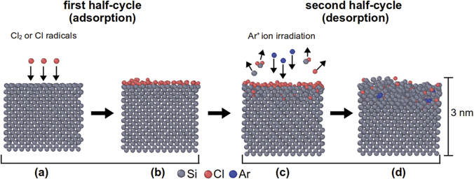
Figure 9. MD simulation results representing anisotropic PE-ALE of Si by surface chlorination. The gray, orange, and blue spheres represent Si, Cl, and Ar atoms. Each block of Si represents a side view of a Si solid with the top edge representing the surface facing the gas phase. The surface region after a Cl-covered Si surface (b) was irradiated by 20 eV Ar+ ions with an ion dose of 1.9 × 1017 cm−2 is given in (d). Reproduced from [118], with the permission of AVS: Science & Technology of Materials, Interfaces, and Processing.
Download figure:
Standard image High-resolution imageIn the second half-cycle, the Cl-adsorbed surface is irradiated with low-energy Ar+ ions. Si atoms bonded with Cl atoms tend to desorb by Ar+ ion impact more easily than surface Si atoms whose Si–Si bonds are not terminated by Cl atoms, because Cl-bonded Si atoms have fewer chemical bonds connected to other Si atoms. In addition, once a Cl atom is bonded with a Si atom, the Si atom's bonds with other Si atoms become weakened because of the high electronegativity of Cl.
Figure 9(d) shows the atomic structures of a surface region after a Cl-covered surface, as shown in (b), was irradiated by 20 eV Ar+ ions with an ion dose of 1.9 × 1017 cm−2, obtained from MD simulations [118]. The details of the simulation techniques are given in reference [118]. It is seen that, even with such low-energy ion exposure, the crystalline Si layer was damaged and amorphized down to a depth of about 1 nm. In addition, Cl atoms are observed to remain (together with some Ar atoms) in the amorphized layer. These Cl atoms were pushed inwards from the top surface by knock-on collisions caused by the incident ions. Such Cl atoms may accumulate after each ALE cycle and remain as impurities at the end of the ALE process.
In some Si PE-ALE processes, a Cl2 plasma, rather than a Cl2 gas, is used in the first half-cycles. Under such conditions, a much thicker Cl–Si mixed layer is formed in the adsorption step because of the impact of Cl+ ions accelerated by the plasma potential (even without external substrate biasing) [118]. Depending on the ion energy, some etching can also take place by the Cl2 plasma irradiation in the first half-cycle.
ALE of Si by chlorine exposure can alternatively be achieved by thermal ALE. Because Cl atoms adsorbed on a Si surface can desorb as SiCl2 when the surface temperature is higher than 650 °C [119], heat, rather than Ar+ ion irradiation, can be used to desorb Cl-bonded Si atoms from the surface in the second half-cycle, which was demonstrated by Imai et al [120] This thermal ALE process was performed with surface temperature modulation between room temperature for Cl adsorption and a temperature of 750 °C for efficient removal of a fraction of a monolayer Si.
2.5. SiO2 ALE
FC plasmas are used to etch SiO2 selectively over Si and SiN in RIE. This is because FC radicals can react with SiO2 and form volatile species such as SiF4, CO, and CO2 whereas they tend to form an FC polymer inhibition layer on Si and SiN surfaces. Based on this knowledge, anisotropic PE-ALE of SiO2 can be constructed by splitting FC surface reactions and ion impact of RIE, i.e., using FC radical adsorption in the first half-cycle and low-energy Ar+ ion irradiation in the second half-cycle. There have been various studies of PE-ALE of SiO2 with such half-cycles [106, 110, 121–127]. In the adsorption half-cycle of an FC-based SiO2 PE-ALE, a thick FC layer can be deposited on the SiO2 surface, depending on the duration of the adsorption half-cycle. Too thick an FC layer can impede the ion-driven etching reactions in the subsequent desorption step and may lead to an etch stop [125, 126]. This contrasts with PE-ALE of Si with halogen adsorption, where the halogen adsorption is typically self-limiting and no thick halogen layer can be formed on the surface at room or higher temperature.
2.6. SiN ALE
The first PE-ALE of SiN was performed by Matsuura et al [128], using excited hydrogen gas (i.e., neutral gas of an Ar/H2 plasma) in the first half-cycle and Ar/H2 plasma in the second half-cycle. However, in this process, the first half-cycle was not an adsorption half-cycle; N atoms of the SiN surface were removed by reactive H atoms, possibly forming NH3 in the first half-cycles. Because H radicals do not etch Si atoms in the underneath layer, the first half-cycle was self-limiting. In the second half-cycle, the remaining Si atoms in the outermost layer were removed by low-energy Ar+ ion irradiation selectively over the underlying SiN surface. In later studies of PE-ALE of SiN, H2 plasmas were used to modify the SiN surface in the first half-cycle and fluorine-based plasmas, such as SF6 or NF3 plasmas, were used in the second half-cycle [129–131].
Although SiN can be etched by FC plasmas with highly energetic ion bombardment [44, 132], hydrofluorocarbon (HFC) plasmas are widely used for RIE of SiN with high selectivity over Si and SiO2 [47, 133–135]. Here HFC reactions with a SiN surface are considered to form volatile species such as SiF4, NH3, and HCN. Such reactions can be used to construct anisotropic PE-ALE of SiN by using HFC deposition in the first half-cycle and Ar plasma irradiation in the second half-cycle [127, 136–140]. If the incident ion energy is not sufficiently high, HFC polymers may accumulate after several ALE cycles and an etch stop may occur [138]. By increasing the Ar+ ion energy in the desorption step, such an etch stop may be avoided but physical sputtering of SiN by the energetic Ar+ ions can ensue after the HFC layer is completely removed, meaning that the second half-cycle is not self-limiting [141].
Isotropic ALE of SiN has been also developed with HFC surface modification. Shinoda et al demonstrated ALE of SiN, using radicals generated from CHF3/O2 plasma in the first half-cycle and heating the surface by infrared irradiation up to 100 °C in the second half-cycle [142–144]. This process is based on the earlier observations that, when a SiN film was exposed to CHF3/O2 plasma or a hydrogenated and oxygenated SiN film is exposed to CF4 plasma, an ammonium fluoride (NH4F) or ammonium hexafluorosilicate ((NH4)2SiF6) film was formed [145, 146]. The presence of oxygen seems necessary for the formation of the salt. In this isotropic ALE process, the top SiN layer is converted to (NH4)2SiF6 during the first half-cycles and then it sublimates in the second half-cycles.
2.7. ALE of metals, metal oxides, and metal nitrides
PE-ALE has been also used to etch metals, metal oxides, and metal nitrides [147–152]. Some metals and metal oxides are known to be 'difficult to etch' in dry processing because byproducts of these materials formed in halogen-based plasma processes are typically non-volatile. However, chlorine exposure has been used to modify the surfaces in the first half-cycle of anisotropic PE-ALE of Cr [153], HfO2 [147], GaN, AlGaN [149], and TaN [151, 152]. Ar+ plasma irradiation took place in the second half-cycle. For some metal oxides, the presence of hydrogen (H) atoms enhances the etch rate by Ar+ ion bombardment [58, 64, 65, 154–157]. For example, in anisotropic PE-ALE of LaAlSiOx [148], Sn-doped In2O3 (ITO) [150], and TaN [151, 152], the surface was modified by hydrogen plasma irradiation in the first half-cycle.
For ALE of metal and metal oxides, various isotropic ALE has been proposed and studied. Metal oxides can be etched with ligand exchange reactions [22, 158–160] or the formation of metal complexes with gaseous organic molecules [161–168]. If plasmas are used in at least one of the half-cycles of such isotropic ALE process, the process may be called (radical-driven) PE-ALE [169, 170]. Although thermal or radical-driven PE-ALE is generally isotropic, anisotropic etching can be achieved with additional ion impact. For example, one can use an oxygen plasma with ion impact to preferentially oxidize a metal surface in the direction of oxygen ion incidence and etch the oxidized surface by thermal desorption, which results in anisotropic etch. For example, Chen et al used oxygen plasma to form a thin oxide layer of a magnetic or noble metal and removed it by organic chemical etching [161].
3. Plasma deposition for nanoscale electronics
3.1. PE-ALD: new opportunities by surface-controlled reactions
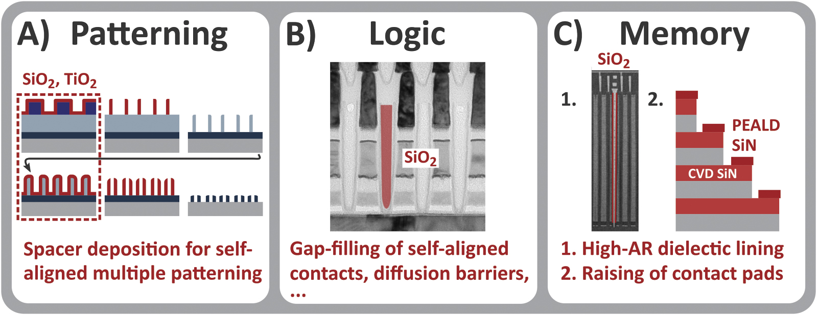
While PE-CVD continues to be in high demand in semiconductor device manufacturing such as the deposition of layers of the SiO2 and SiN pairs (i.e. ONO layers) of 3D NAND devices, PE-ALD is becoming an increasingly important technique for the continued downscaling of nanoelectronic devices. This will be illustrated in this subsection with a selection of representative applications in nanoelectronics. Some key challenges in thin film deposition, i.e., uniformity, conformality, thickness control and low-temperature processing, are highlighted in figure 10 for several applications, which all rely on PE-ALD as their solutions. First, in self-aligned multiple patterning (A), the sidewall spacers (typically SiO2 or TiO2) need to be deposited with a high film conformality and a precise thickness to ensure accurate reproduction of the desired pattern [171]. Moreover, because of issues related to the film stress and the presence of temperature-sensitive photoresist, the spacers typically have to be deposited at a low temperature [172]. These requirements necessitate the use of PE-ALD for this application [173]. Thermal ALD could offer a high film conformality and precise thickness control but it often requires a high surface temperature. On the other hand, PE-ALD of SiO2 can provide high-quality SiO2 even at low and moderate temperatures (e.g., at 50 °C) [174, 175]. Since self-aligned multiple patterning schemes are indispensable for the fabrication of present-day technology nodes, this application of PE-ALD currently represents one of the largest segments of the global ALD market [25].

Figure 10. Examples of applications of PE-ALD in patterning, logic device fabrication, and memory device fabrication. The layers prepared by PE-ALD are indicated in (dark) red. In these examples, i.e., self-aligned quadruple patterning (A), gap-filling (B), and dielectric lining (C, left), the film conformality, thickness control, and material quality provided by PE-ALD are essential [1, 171, 176–178]. PE-ALD is also used for the raising of contact landing pads in 3D NAND devices, by topographically-selective deposition of SiN (C, right). The stack of SiO2 and SiN pairs in 3D NAND devices are deposited by PE-CVD. (B) Reproduced with permission from [179]. TEM images: courtesy of ASM. (C) Reproduced with permission from [180]. © 2017 MSSCORPS CO., LTD. All Rights Reserved.
Download figure:
Standard image High-resolution imageSecond, in logic devices (figure 10(B)), one of the key applications of PE-ALD is gap-filling, for instance, of diffusion barriers and regions around (self-aligned) contacts. There, the high film conformality and material quality provided by PE-ALD are exploited for achieving a seamless and high-quality fill [176–178], possibly in combination with other approaches such as inhibitor dosing [181] and PE-CVD [178]. This application of PE-ALD is also found in the fabrication of memory devices, where PE-ALD of SiO2 and TiO2, for instance, have been reported to be used for the gap-filling of electrical isolation regions [176–178].
Finally, as mentioned in the introduction, the ability to deposit nanometer-thin films with excellent conformality is also essential in the fabrication of 3D NAND devices, as illustrated in figure 10(C). There, PE-ALD enables the growth of high-quality and conformal SiO2 liners in the increasingly deep channels, which currently have an AR of 40 to 60 [1]. Another challenge in 3D NAND device fabrication is the raising of the SiN contact landing pads in the 3D NAND staircase. This challenge is representative of the growing need for advanced processing methods such as area-selective [182, 183] and topographically-selective [184–186] deposition. Raising the contact landing pad, through the precise application of an additional layer of SiN, makes it easier for the metal contact etch to end within the landing pad. At the same time, the deposition of SiN on the sidewalls must be avoided to make sure that the horizontal SiN layers remain isolated from each other. (Note that the SiN is sacrificial and is later replaced by W to form the word lines [187]). Topographically-selective deposition of SiN with precise thickness control is therefore required. It has been reported that PE-ALD of SiN is used for this purpose [1], where the influence of directional ion bombardment is exploited for achieving topographic selectivity.
3.2. Fundamentals of PE-ALD: roles of radicals and ions
In this subsection, we discuss key aspects of the roles that radicals and ions play in PE-ALD used in the applications discussed in the previous subsection. Figure 11 highlights the surface reactions taking place in typical PE-ALD processes. As illustrated in figure 11(A), a wide variety of species are present in a plasma used in PE-ALD, such as radicals, ions, photons, electrons, metastable species, and (dissociated) reaction products [25]. To tailor their influence, the composition of the plasma can be controlled to a certain level, for instance, by adjusting the input power and gas pressure. Radicals are considered to be essential for film growth while ions can have a significant influence by transferring energy and momentum to the surface. The effects of free electrons and photons are generally considered to be limited although electrons can assist, e.g., the desorption of surface species [188], and (ultraviolet) photons can enhance surface reactions, as in photon-assisted ALD [189], and/or damage the depositing film surfaces of sensitive electronic devices [83, 190]. Surface charging may play a role during plasma ALD, as is known for (HAR) plasma etching [93]. Regarding the role of radicals, figure 11 shows why information on the loss of radicals through surface recombination is essential for controlling the process results on substrates with HAR features (figure 11(D1)). Figure 11 also illustrates the (potentially beneficial) influence of ions on the properties of films grown by PE-ALD. These radical and ion effects are important for PE-ALD on flat surfaces as well as 3D structures. In such 3D structures, the film conformality and topographically-selectiveness of PE-ALD are affected by such radical and ion properties (figure 11(D2)).
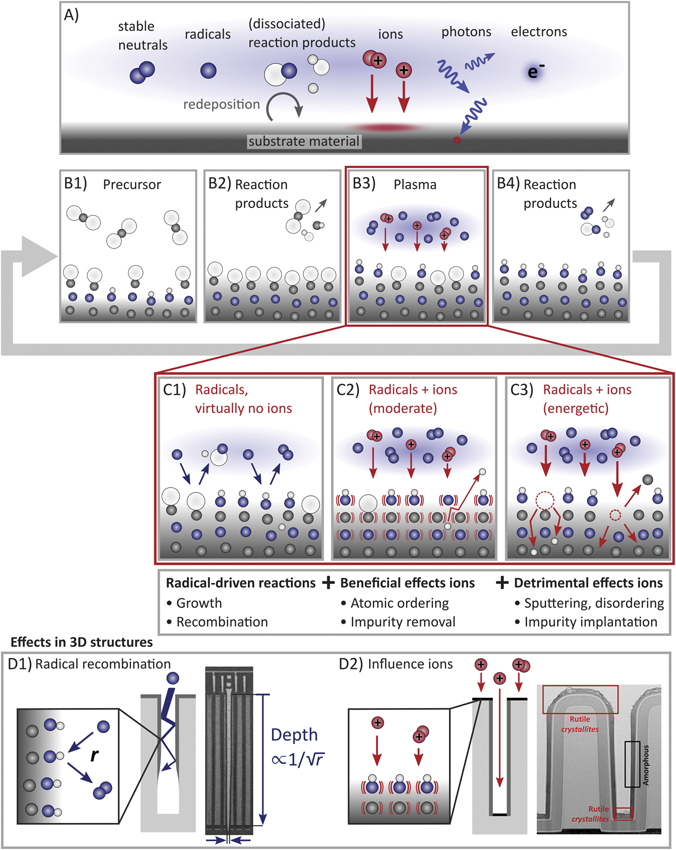
Figure 11. Overview of surface reaction mechanisms in typical PE-ALD. The individual panels illustrate: (A) typical gas-phase species in plasma, (B) a generic PE-ALD cycle, (C1) surface reactions leading to the growth (left) or recombination of radicals (right), (C2) beneficial effects of ions, such as atomic ordering and impurity removal, and (C3) potential detrimental effects of ions. The bottom frame highlights radical and ion effects on 3D structure fabrication. i.e., (D1) the loss of radicals by surface recombination, where the surface recombination probability r limits the depth up to which conformal film growth is feasible, and (D2) directional ion bombardment, which mainly impacts film growth on the horizontally-oriented surfaces rather than the vertical sidewalls. (D1) Reproduced with permission from [180]. © 2017 MSSCORPS CO., LTD. All Rights Reserved. (D2) Reprinted with permission from [186]. Copyright (2018) American Chemical Society.
Download figure:
Standard image High-resolution imageFirst, we discuss the role of radicals during PE-ALD. Radicals can be atomic species such as O, H, and N or molecular fragments such as NH and NH2. They are highly reactive and numerous under typical plasma conditions [191, 192], and therefore commonly considered to be the driving species for the film growth in PE-ALD [25, 193, 194]. During PE-ALD of oxides, for instance, atomic oxygen can assist in the removal of precursor ligands and the production of hydroxyl groups at the surface [195–197]. This can happen through a wide variety of reaction pathways, such as a combination of decomposition- and combustion-like reactions [195, 196]. While the exact reaction pathways are generally difficult to pinpoint experimentally [195, 196], theoretical studies support that such radicals play an important role. As an example, table 1 shows the overall reaction energies of O radicals interacting with a methylated alumina surface, determined by Fomengia et al [197] with density functional theory calculations. These reactions are representative of those in PE-ALD of Al2O3 using Al(CH3)3 and O2 plasma. The study shows that a range of barrierless and highly exothermic reaction pathways are possible in the process and these reactions ultimately lead to the formation of surface hydroxyl groups and different gaseous byproducts [197].
Table 1. Total reaction energies of O atoms reacting with a methylated alumina surface, as reported by Fomengia et al [197] These reaction energies are calculated with the assumption of the formation of hydroxyl groups and a selection of gaseous byproducts as the final states.
| Reaction | ΔE (eV per 1O) |
|---|---|
| (AlCH3)3 + 31O → (AlOH)3 + 3/2 C2H2 | −7.41 |
| (AlCH3)3 + 61O → (AlOH)3 + 3CH2O | −6.61 |
| (AlCH3)3 + 91O → (AlOH)3 + 3CO + 3H2O | −6.59 |
| (AlCH3)3 + 121O → (AlOH)3 + 3CO2 + 3H2O | −6.91 |
In addition to the detailed studies highlighted above, the importance of radicals during PE-ALD is also suggested by experimental observations. For example, in cases where the plasma is generated far away from the substrate, which is often referred to as radical-driven ALD, high-quality film growth has been reported to occur with a minimal flux of ions, electrons, and photons [198]. Similarly, a recent study has shown that film growth by PE-ALD can be achieved deep into horizontally-oriented cavity structures, without any contribution of ions or photons [199].
Although the high reactivity of radicals is favorable for film growth, radicals are not chemically stable and tend to be lost through recombination reactions. For example, upon the interaction with a surface, atomic oxygen can recombine with another oxygen atom to form a stable molecule O2, as illustrated at the right of figure 11(C1). The loss of radicals through surface recombination can be a key limiting factor for achieving film growth deep inside HAR structures [199–204]. As illustrated in figure 11(D1), highly reactive radicals may not reach the bottom of a deep and narrow feature if they have a high surface recombination probability r [199–204]. Consequently, an extended plasma exposure may be required for reaching saturation at the bottom, such that the conformal film growth may not be feasible under reasonable circumstances [199, 202]. Based on the recent work of reference [199], the plasma exposure time needed to reach saturation on a HAR trench is similar to that of a planar substrate if the AR of the trench is lower than  , with r being the surface recombination probability of the radical at the deposited material. Here, the material of the substrate (e.g., Si or SiO2) typically does not play a significant role, since the recombination of radicals on the deposited material becomes the main factor limiting the transport of radicals into the HAR structure [199]. This implies that PE-ALD on a trench with an AR of 100 is feasible if r < 10−4. On the other hand, if
  , the film growth at the bottom of the trench is significantly impeded by the loss of radicals through surface recombination on the sidewalls, and the saturation time tsat strongly depends on the AR as
  [199]. Information on the value of r is therefore crucial for an understanding and control of the throughput and feasibility of PE-ALD in HAR applications.
The impact of radical recombination on the surface is further illustrated in figure 12, which presents the parameter space where the conformal film growth over a trench by PE-ALD is feasible (white region) and unfeasible (red region), depending on the AR of the trench and the surface recombination probability r of an O atom. The boundary indicates the largest AR values of a trench on which conformal film growth by PE-ALD is expected to be feasible, in terms of the required plasma exposure time, as a function of r. Conformal film growth is labeled 'feasible' if the required plasma exposure time is shorter than 10 times the plasma exposure time needed for a planar substrate (mathematically, the boundary of the red region has been estimated as  ) [199]. It should be noted that, the lower the surface recombination probability r is, the higher the trench AR becomes on which the conformal film growth becomes feasible. The value r is highly dependent on the depositing film material and can be very low in certain cases, such that the feasible AR up to 1000 could be reached. In particular, figure 12 indicates that PE-ALD of SiO2 in the fabrication of 3D NAND devices, where the channels have an AR of approximately 40 to 60 [1], is barely affected by the radical surface recombination. This means that the conformal deposition of SiO2 on the channel sidewalls with much higher ARs is also possible with PE-ALD.
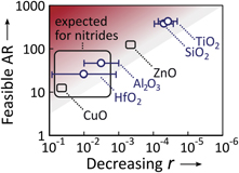
Figure 12. The parameter space of the AR of a trench and the surface recombination rate r of an O atom where the conformal film growth on the trench by PE-ALD is feasible (white region) and unfeasible (red region). The gray boundary region indicates the largest AR values of a trench on which conformal film growth by PE-ALD is expected to be feasible (i.e., achieved within <10 times the plasma exposure time needed for a planar substrate) as a function of the surface recombination probability r. The recombination probability r depends on the deposited material and reference materials are listed for some r values. The values of r were determined from the decay in radical density into a coated tube (black squares) [206] and the film penetration into HAR structures during PE-ALD (blue circles) [199, 204]. In addition, an expected range for PE-ALD of nitrides is indicated, which is based on values of r reported for the surface recombination rates of H atoms on various nitride materials [201].
Download figure:
Standard image High-resolution imageRegarding the exact values of r, it should be noted that experimental conditions such as the surface treatment [205, 206], roughness [207], plasma pressure [199], substrate temperature [199, 207, 208], and the flux of ions [200] all can have a considerable influence. Yet, so far most data on r reported in the literature have been determined under conditions that are not representative for PE-ALD on HAR structures (e.g., from the spatial or temporal decay in radical density inside a tube of the investigated material) [205–209]. More representative values of r that adequately describe the consequences for film conformality during PE-ALD can be determined directly from the achieved film penetration into HAR structures [199, 204]. The data indicated as blue circles in figure 12 were determined using this method [199, 204].
Next, we discuss the influence of ions during PE-ALD. In several studies on PE-ALD of oxides as well as nitrides [186, 210–218], a significantly beneficial influence of ions has been reported, such as impurity removal, densification [219], and crystallization (illustrated in figure 11(C2)). On the other hand, unfavorable effects such as sputtering, amorphization, and impurity implantation (illustrated figure 11(C3)) can be present when the supplied ion energy or dose is too high [186, 193]. These effects were previously investigated with the increase of ion energy up to approximately 100 eV or even higher [184, 186, 220]. However, ions with a relatively low energy of ∼10 eV were also observed to have a significant influence [215, 218]. The often favorable effect of ions impinging on the surface during PE-ALD is somewhat similar to the influence of temperature. Both higher temperature and higher ion flux or energy can facilitate chemical reactions and enhance some physical effects such as atomic ordering by raising the overall kinetic energies of the surface atoms. However, the mechanisms by which the energy is transferred are very different between temperature and ion kinetic energy. Most importantly, the kinetic energy of ions impinging on the surface (and the energy associated with their ionization state) [193, 221] is transferred only to the top few nanometers of the deposited film with highly local and intense energy pulses that quickly dissipate [222, 223]. As a result, ions can induce high-temperature effects on the surface, without increasing the substrate temperature. Another key difference is that ions carry momenta and therefore may induce other physical effects such as sputtering.
Since ions often have a considerable impact during PE-ALD, it is crucial to understand what controls the influence of ions. This is not trivial since parameters such as the ion energy, ion flux, and plasma exposure time all can have individual effects. Still, depending on the process, it may be possible to capture the combined effect of these parameters in terms of a single, universal parameter that can be used to precisely exploit the effect of ions. A recent study on SiO2 PE-ALD [215] suggested that the supplied ion energy dose (eV nm−2 cycle−1), calculated as the product of the mean ion energy, ion flux, and plasma exposure time per ALD cycle [220], could be used as such a universal parameter. In that work, the acquired growth per cycle (GPC) showed a clear trend as a function of the supplied ion energy dose under a wide variety of plasma conditions (see figure 13(A)).

Figure 13. Examples of how the growth behavior in PE-ALD can be influenced by higher ion energy or dose. For PE-ALD of SiO2, a seemingly universal trend with the ion energy dose, i.e., the product of the mean ion energy and the ion dose, has been reported [215]. In contrast, for PE-ALD of SiN, higher ion energy does not give the same results as a higher ion dose [220]. This may be caused by the presence of other physical effects with energy thresholds such as surface crystallization or sputtering.
Download figure:
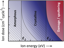
Standard image High-resolution imageStill, such a universal trend with the ion energy dose is not observed for all PE-ALD processes. In a different study on PE-ALD of SiN, for instance, an extended plasma exposure time did not give the same results as those with higher ion energies while the provided ion energy dose was the same in both cases (see figure 13) [220]. This suggests some other physical effects such as surface crystallization or damage formation by physical sputtering also affect the GPC. Such effects can take place only if the incident ion energy is higher than a certain threshold energy. Similar energy thresholds are also present in plasma etching [21, 32] and can be linked, for instance, to atomic displacement or the activation of ion-induced chemical reactions [193, 220]. The energy thresholds associated with physical effects are related to the binding energy of the surface material and are likely to lie in the range approximately from 20 to 50 eV for the displacement of surface atoms (due to collision cascade effects, the thresholds are typically 5–10 times the binding energy) and approximately from 40 to 100 eV for the displacement of bulk atoms [220].
Corresponding to the aforementioned observations, it is speculated that the influence of ions during PE-ALD generally follows a trend as illustrated in figure 14. This figure, which is inspired by the recent review of Boris et al [193], shows a contour map of the type of growth that may be expected when supplying a certain ion dose (cm−2 cycle−1) and ion energy (eV). Following figure 14, a similar growth behavior is generally expected along the diagonal lines that correspond to a constant ion energy dose (eV cm−2 cycle−1). However, when other effects such as crystallization (whose threshold energy is denoted as E1 in figure 14) or physical sputtering (E2) are involved, a higher ion dose may no longer give growth behaviors similar to those with a high ion energy. This means that the lines of constant material properties deviate from the diagonal lines.
Figure 14. Contour map illustrating the potential influence of the supplied ion dose and ion energy on the growth behavior during PE-ALD. In this figure, similar growth behaviors are generally expected along diagonal lines where the product of the ion energy (eV) and ion dose (cm−2 cycle−1) is constant. However, if other effects such as crystallization (whose threshold energy is denoted as E1) or physical sputtering (E2) are involved, a high ion dose may no longer give growth behaviors similar to those with a high ion energy. This figure is inspired by the recent review of Boris et al [193].
Download figure:
Standard image High-resolution image
Although a schematic diagram such as figure 14 can be used as a rule-of-thumb, more information is required to understand the details of the influence of ions during PE-ALD. This includes further insight into the presence of synergetic effects [224] and the exact values of possible energy thresholds. When such energy thresholds are known, accurate ion energy control could provide new opportunities, for instance by activating beneficial effects without simultaneously exceeding the energy threshold related to structural damage [225]. Precise control over the supplied ion energies can be achieved, for example, by tailored waveform biasing. This method was pioneered by Wendt and co-workers [226, 227] and further explored by several others to control the ion flux energy distribution function (IFEDF) of the ions in remote plasmas [228–231]. Voltage waveform tailoring was also transferred to CCPs to control the ion energy [232–236]. The technique of fine-tuning the IFEDF [237] is currently explored for applications in PE-ALE [231] but also RIE could likely benefit from it to improve etch selectivity. The method would also be helpful to identify and exploit ion energy thresholds present in atomic-level plasma etching and deposition.
Accurate control over the influence of ions is also a key to achieving film conformality [218] and topographically-selective processing [184–186]. Since ions impinge on the substrate anisotropically, impinging ions can have a direct influence on the deposited film conformality [218], as illustrated in figure 11(D2). This effect can be mitigated by the reduction of ion flux and energy [215, 218]. On the other hand, the effect of directional ion bombardment can be exploited for topographically-selective processing. For example, an ion-induced increase in etch rates (e.g., by structural damage) can be used to remove the material only from the surfaces that were exposed to the ion incidence in the half-cycles with plasma step (i.e., the horizontal bottom and top surfaces but not the vertical sidewalls) [186]. In contrast, an ion-induced reduction in etch rates (e.g., through densification) can be used to preserve the ion-exposed surface material (e.g., for the raising of contact landing pads in 3D NAND devices) [185]. This exemplifies how a detailed understanding of the role of the ions can advance PE-ALD techniques for various processing applications.
4. Conclusions and prospectives
We have discussed a selection of fundamental challenges for plasma processing techniques relevant to nanoelectronics. Due to the continuous reduction of device dimensions, the growing need to build complex 3D device structures, the increasing number of new kinds of materials used in devices, and the increasing integration complexity, methods with atomic-level control and, more particularly, surface-controlled techniques such as PE-ALE and PE-ALD are becoming essential for achieving the required precision in etching and deposition processes.
Plasma-based techniques involve non-thermal equilibrium chemical reactions in the gas phase and on the surface. This means that the energy needed to activate surface chemical reactions for etching and deposition is provided by the reactivity of incident radical and ionic species, rather than by just heat applied to the substrate. Therefore plasma-based techniques are well suited for low-temperature processing. The momentum transfer from incident ions to the surface also provides another degree of freedom, which enables anisotropic processing. The availability of reactive ions and radicals offers a far wider variety of surface chemical reactions that can be exploited to achieve desired etching and deposition results that are not available in thermal processes.
In conventional plasma processing such as RIE, PE-CVD, and PVD, the surface reactions are mostly controlled by the incident fluxes of plasma-generated species. In other words, the etch or deposition rates are typically proportional to such fluxes. These processes do not allow precise control of etched depth or deposition film thickness over material surfaces of complex 3D structures because the incident fluxes can vary significantly over the locations, depending on the local view angles that may be limited by the surrounding 3D structures. Unlike such conventional processes, atomic layer processes are surface-controlled and typically allow highly uniform isotropic or anisotropic processes over a large area, regardless of the view angles. In this article, the discussion was mostly focused on PE-ALE and PE-ALD.
There are two types of PE-ALE; anisotropic PE-ALE and isotropic PE-ALE. First, we discussed the similarity between RIE and anisotropic PE-ALE. Surface chemical reactions used in anisotropic PE-ALE are often the same as those used in RIE. The main difference is that, in anisotropic PE-ALE, chemical modification of the surface is separated from the removal of surface materials by ion impact, and the cycle of chemical modification (adsorption step) and etching (desorption step) is repeated many times until the targeted etched depth is achieved. Because the half-reactions are self-limiting, anisotropic PE-ALE is able to achieve more precise etching of a material selectively over other materials as compared to RIE. Second, we discussed examples of Si, SiO2, SiN, and metal/metal oxide etching by anisotropic PE-ALE. If plasma-generated radicals rather than ions play an essential role in the surface chemical PE-ALE reactions, the process can result in isotropic PE-ALE. Although we have not considered such processes in detail in this article, this is another growing field of ALE that will become important in future semiconductor technology nodes.
For PE-ALD, we highlighted the roles of radicals and energetic ions in the manufacturing processes of state-of-the-art nanoelectronics devices. Radicals are essential for film growth but can be lost in deep and narrow structures by surface recombination on the sidewalls. Because the surface recombination probability of a radical species depends strongly on the depositing surface material, an understanding of the surface recombination probability is essential in controlling PE-ALD processes for HAR applications. Energetic ions can also have considerable and often beneficial effects on film growth by transferring their energy and momentum to the surface. More specifically, we discussed the dependence of film growth behavior, including the growth rate, on the supplied ion energy dose as well as other physical effects such as crystallization and sputtering. The crystallization and sputtering can be triggered when the incident ion energy exceeds the corresponding threshold energies.
These results illustrate how a fundamental understanding of basic reaction mechanisms is crucial for achieving the atomic-level precision of plasma-based atomic layer processes required for next-generation nanoelectronics device manufacturing. For PE-ALE, achieving higher etch rates and high selectivity for a wide range of materials and, for PE-ALD, further development of area-selective and topographically-selective processing are considered to be some of the most important technical challenges. In addition, further research is needed to improve the overall efficiency of atomic layer processes to meet the growing demand from advanced nanoelectronics device manufacturing.
Acknowledgments
The work of KA, HCMK, AJMM, and WMMK was partially supported by the Netherlands Organization for Scientific Research (NWO) through the program HTSM with Project No. 15352 and Project No. 17124. The work by SH, TI, and KK was partially supported by the Japan Society of the Promotion of Science (JSPS) Grants-in-Aid for Scientific Research (A) (No. 21H04453) and (C) (No. 21K03522), and the JSPS Core-to-Core Program (No. JPJSCCA2019002).
Data availability statement
All data that support the findings of this study are included within the article (and any supplementary files).
Author contributions
KA and SH contributed equally to this paper. All authors listed have made substantial and intellectual contributions to the work. KA wrote the first draft of this article except for section 2 with the help of WMMK, HCMK, and AJMM and SH wrote the first draft of section 2 with the help of TI and KK. WMMK and SH reviewed, revised, and finalized the draft.