

Abstract
Producing hydrogen fuel using suitable photocatalysts from water splitting is a feasible method to harvest solar energy. A desired photocatalyst is expected to have suitable band gap, moderate band edge position, and high carrier mobility. By employing first-principles calculations, we explore a α-CS monolayer as a metal-free efficient photocatalyst. The α-CS monolayer shows good energetic, dynamic, and thermal stabilities and is insoluble in water, suggesting its experimental practicability. Monolayer and bilayer α-CS present not only appropriate band gaps for visible and ultraviolet light absorption but also moderate band alignments with water redox potentials in pH neutral water. Remarkably, the α-CS monolayer exhibits high (up to 8453.19 cm2 V−1s−1 for hole) and anisotropic carrier mobility, which is favorable to the migration and separation of photogenerated carriers. In addition, monolayer α-CS experiences an interesting semiconductor-metal transition by applying uniaxial strain and external electric field. Moreover, α-CS under certain strain and electric field is still dynamically stable with the absence of imaginary frequencies. Furthermore, we demonstrate that the graphite (0 0 1) surface is a potential substrate for the α-CS growth with the intrinsic properties of α-CS maintaining. Therefore, our results could pave the way for the application of α-CS as a promising photocatalyst.
Export citation and abstract BibTeX RIS
1. Introduction
Solar energy is the cleanest and most abundant source of renewable energy. However, in view of the diffuseness and intermittency of insolation, solar energy utilization requires solar capture, storage and further conversion. The conversion of solar energy into fuel through photocatalyzed water splitting to produce hydrogen is an effective approach [1–3]. Because water is the most abundant source of hydrogen, the design of feasible photocatalysts for getting molecular H2 from water splitting has become one of the main challenges. A perfect photocatalyst material should satisfy the following criteria: suitable band gap (1.5–3.0 eV), efficient visible light absorption, excellent carrier mobility, and band edge positions straddling the water redox potentials [4–6].
According to the above criteria, a series of novel photocatalysts based on two-dimensional (2D) materials have been explored. Compared with bulk materials, 2D materials provide intrinsic advantages, such as large surface/volume ratio, fast mobility of charge carriers, and rich option of host-guest species [7, 8]. Generally, there are two types of 2D photocatalyst materials, i.e., metal-containing and metal-free. Numerous 2D metal oxides, e.g., TiO2, ZnO, and WO3, have exhibited excellent performance in energy and environmental-related applications [9–13]. Nevertheless, the metal oxide nanosheets have wide band gaps and adsorb light mainly in the UV region. One of the most effective approaches to narrow the band gap is doping of non-metal and metal ions [14, 15]. However, the photocatalytic activities of the doped photocatalysts are usually not high because the doping levels act as carrier recombination centers. A strategy for enhancing the charge carrier separation is to use noble metal particles loaded onto the semiconductor surface [16, 17]. However, the high cost (e.g., Pt, Au) and toxicity (e.g., Pb) of cocatalysts bring potential issues in the mass production and environmental protection, respectively. Consequently, metal-free photocatalysts have been explored and studied extensively [14].
In recent years, group-IV 2D materials can be used in some important physical and chemical processes because of their high carrier mobility and excellent mechanical performance [18]. However, the absence of band gap is one of the major drawbacks of these materials, limiting their high photocatalystic performances as photocatalysts. Therefore, various strategies have been proposed, such as doping with non-metal elements or forming binary complexes with group-VI elements [19–24]. For example, S-doping can improve the activity and selectivity of graphene for oxygen reduction reactions, whereas the band gap of S-doped graphene sensitively depends on the content of sulfur [25]. On the one hand, monolayer group IV–VI monochalcogenides have been found to be wide-band-gap semiconductors [22, 23]. For instance, monolayer SnS possesses an appropriate band gap of 2.04 eV, while its band edge of the valence band maximum (VBM) even under a strongly basic condition (pH = 12.0) cannot straddle the oxidation potential [22]. Recently, the synthesized α-sulfur crystals have been visible-light photocatalysts, but the photocatalytic activity was low due to the large particle size [26]. It is natural to ask a question: whether there exists a new IV–VI nanomaterial as a metal-free photocatalyst satisfying the above criteria.
In this study, based on first-principles calculations, we predict a stable α-CS monolayer. The results present that monolayer α-CS is an indirect semiconductor (1.96 eV) with high carrier mobility (up to 8453.19 cm2 V−1 s−1 for hole along the armchair direction). In addition, it shows strong light absorption in the ultraviolet and visible regions. Furthermore, the band edges of both VBM and conduction band minimum (CBM) of monolayer/bilayer α-CS straddle the water redox potentials in pH neutral water, indicating that monolayer and bilayer α-CS are potential photocatalysts for water splitting.
2. Computational details
2.1. Optimization (properties) calculation
All first-principles calculations are performed based on the norm-conserving pseudopotential [27] and Perdew–Burke–Ernzerh (PBE) exchange–correlation functional [28] as implemented in the Cambridge Serial Total Energy Package [29]. Because the PBE functional always underestimates the band gap of semiconductors, we also use the Heyd–Scuseria–Ernzerhof screened hybrid functional (HSE06) [30] to correct the band structure. A cutoff energy of 1500 eV is used for the plane-wave basis set. The k-points of the Brillouin zone are sampled with 0.02 (0.01) Å−1 spacing for the geometry optimization (properties calculation). A large vacuum space of 20 Å is chosen to avoid the interlayer interaction between layers (along the c-axis). Considering the effect of dispersion interaction between layers, the van der Waals calculations based on the Tkatchenko–Scheffler approach is performed [31]. The tolerances of energy and force are 5 × 10⁻⁷ eV/atom and 0.001 eVÅ−1, respectively. The linear response method is used for the phonon dispersion calculations [32].
2.2. Ab initio molecular dynamics
Furthermore, to clarify the thermal stability of α-CS, the ab initio molecular dynamics simulations are performed at temperatures of 800, 1000, and 1200 K in the canonical ensemble. To explore the stability of α-CS in liquid water, a conductor-like screening model (COSMO) [33] is used to simulate a H2O solvent environment at 300 K. In this canonical ensemble, a 3 × 3 supercell (36 atoms) is used, and the total simulation time is 10 ps with a time step of 1 fs.
2.3. Carrier mobility and in-plane stiffness
The carrier mobility of 2D materials based on deformation theory (DP) theory proposed by Bardeen and Shockley can be expressed as the following formula [34]:
In this equation, e, KB, T, C2D, E1, and m* are electron charge, Boltzmann constant, temperature (300 K), in-plane stiffness, deformation potential constant, and effective mass, respectively. The C2D is defined as  , where E0 is the total energy of cell without dilation and S0 is the equilibrium lattice area. The strain step is 0.5%. The average effective mass md is determined by
  . The term E1 is defined by
  , which represents the energy of CBM for electrons and the VBM for holes along the transport (a and b) direction. ΔV is the conduction band or valence band energy change under certain strain.
  is the lattice constant along the transport direction, and
  is the deformation of
  ·
·  (i = h for holes, i = e for electrons) is based on the effective mass approximation
  .
.
3. Results and discussions
3.1. Structure and stability
We first design five possible 2D configurations of monolayer CS (α, β, γ, δ, and ε) (shown in the ESI). The α-CS is the most energetically stable (figures 1(a) and (b)), which is similar to the α-carbon monosulfide nanostructure [35]. In the primitive cell of α-CS, one C (S) atom binds to two neighboring S (C) atoms. The structure properties of α-CS are listed in table 1. The D0 (1.79 Å) of α-CS is about 0.43 Å shorter than that of black phosphorene [36]. The lattice constants are smaller than those of α-SiS, and GeS [37, 38]. To evalute the stability of α-CS, we first calculate the binding energy (Eb), which is defined by the following formula: Eb = (nEC + nES − Eα-CS)/2n, where the EC (ES) and Eα-CS represent the single point energies of the C (S) atom and α-CS, respectively. n is the number of atoms in the primitive cell. The Eb of α-CS (6.11 eV/atom) is comparable with those of black phosphorene (5.36 eV/atom), α-PN (6.76 eV/atom) and Pmma-CO (7.72 eV/atom) [39–41], indicating that the C–S bonds of α-CS are robust.
Table 1. The lattice constants (Å), bond length (Å), and bond angles (°) of α-CS.
| a | b | C1–S1 (C2–S2) | C1–S2 (C2–S1) | ∠C1S1C2 | ∠S1C2S2 | ∠C2S2C2 |
|---|---|---|---|---|---|---|
| 4.02 | 2.78 | 1.75 | 1.85 | 101.89 | 114.68 | 105.05 |

Figure 1. The top (a) and side (b) views of α-CS with two C atoms (small balls) and two S atoms (large balls) in the primitive cell. (a) and (b) are the lattice constants. (c) Phonon dispersion of monolayer α-CS. (d) Calculated Raman spectra and vibrational modes corresponding to the peaks convoluted.
Download figure:
Standard image High-resolution imageThen, to explore the kinetic stability of α-CS, the calculated vibrational phonon spectrum shows no apparent imaginary modes existing in the acoustic branch frequencies (figure 1(c)). Moreover, the highest optical frequency is up to 848 cm−1, which is higher than those of black phosphorus (~450 cm−1), MoS2 (~500 cm−1), and silicene (580 cm−1) [42–44], suggesting the strong bonding nature of α-CS. It is well known that the Raman spectrum reflects the vibrational modes of atoms and relates to the phonon dispersion. As shown in the Raman spectra (figure 1(d)), the two higher peaks at about 757 and 770 cm−1 are attributed to the in-plane optical vibrational modes mainly arising from the vibration of C atoms. The two lower peaks (356 and 420 cm−1) are corresponding to the out-of-plane acoustic vibrational modes. In addition, at the same calculation level, the Raman spectra of graphene are calculated. The well-known G band appears at 1563 cm−1, which agrees with the experimental value (1582 cm−1) [45]. Our results will provide a fingerprint of verifying the conformation of α-CS in the future experiment.
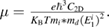
Furthermore, to clarify the thermal stability of dynamically stable α-CS under vacuum condition, the ab initio molecular dynamics simulations are performed. The α-CS is thermally stable at 1000 K. However, at 1200 K, the structure has been destroyed with the bond broken and geometry reconstructed (figures 2(a)–(c)). Hence, α-CS may melt at a temperature between 1000 K and 1200 K. The possible melting point of α-CS is much higher than those of reported p-SiC (600 K) and GeS (500 K) [6, 46]. Furthermore, α-CS as a photocatalyst also needs to be insoluble in water. We further check the stability of α-CS in the water solvent environment at 300 K (figure 2(d)). α-CS can maintain the structure stability in water. The average bond length slightly changes and is nearly 1.19% larger than that under vacuum condition at 0 K. Therefore, our result confirms that the α-CS as a photocatalyst has a good thermodynamic stability.
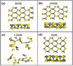
Figure 2. The snapshots of top and side views of the final atomic configurations at 800 K (a), 1000 K (b), and 1200 K (c) under vacuum condition. (d) The final structure at 300 K in the water solvent environment.
Download figure:
Standard image High-resolution imageTo verify the mechanical stability of α-CS, we calculate its linear elastic constants. The necessary and sufficient elastic stability condition of monolayer α-CS can be defined by the following formula [47]:

The values of elastic constants matrix components C11, C22, C66, and C12 are 21.06, 113.14, 0.41, and 14.49 GPa, respectively. Clearly, the elastic constants satisfy the above-mentioned conditions, suggesting that α-CS is mechanically stable. We next calculate the in-plane stiffness (C2D) of α-CS (for more details see next section). The value of C2D is 39.84 (221.76) N m−1, which is about two times than that of black phosphorene (24.26 (103.28) N m−1) along the armchair (zigzag) direction [39]. Therefore, the C–S bonds of the α-CS are robust.
3.2. Electronic structures
The band structures from PBE and HSE06 show α-CS is an indirect gap semiconductor (figure 3(a)). The CBM lies in the Γ point, whereas the VBM locates on the Y–Γ path. The PBE and HSE06 computations give band gaps of 1.11 and 1.96 eV, respectively. Notably, a direct band gap (2.02 eV at the HSE06 level) of α-CS at the Γ point is quite close to the indirect band gap. As recently reported of perovskites, the weakly indirect band gap may be an advantage for photovoltaic materials with strong light absorption and long carrier lifetime [48]. Compared with the band gaps of Cmmm-SiS (1.01 eV), Pma2-SiS (1.22 eV), and α-AsP (0.90 eV) [49, 50], the band-gap of α-CS is more suitable for the visible light absorption.
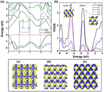
Figure 3. (a) Band structures of α-CS computed by the PBE (green solid line) and HSE06 methods (blue dashed line). The Brillouin zone of α-CS is inseted. (b) The PDOS computed by the HSE06 method. The energy regions from 0 (−4) to −2 (−7) eV are denoted zone I (zone II). The insets show the molecular orbitals corresponding to states in zone I and zone II. The CBM (c) and VBM (d) with the iso-surface value of 0.06 e Å−3. The two (blue and yellow) colors denote ± signs of the wave function. (e) The difference charge density of α-CS. Blue and yellow represent the electron accumulation and depletion region, respectively.
Download figure:
Standard image High-resolution imageAt the near Γ point, the energy of the states of the top valence bands is suppressed, resulting in the shifting of VBM from Γ to a near k point. The top valence band shows a Mexican-hat-like dispersion around the Γ point. As presented in figure 3(b), this unique feature of band structure leads to both a high density of states (DOS) and an almost one-dimensional-like van Hove singularity. The projected DOS reveals that the Mexican-hat-like valence bands near the Fermi level are predominantly contributed by C-2p orbitals. In detail, the valence bands below the Fermi level consist of zone I and zone II. The zone I is mainly contributed by the 2p states of C atoms and partly by the 2p states of S atoms, exhibiting a π-type antibonding character (shown in the inset of zone I). At the energy region of −4 to −7 eV (zone II), the p orbitals of C and S atoms are hybridized, which indicates that the in-plane σ-type covalent bonding character between C and S atoms (the inset in zone II). Furthermore, the σ-bonding strength between C and S atoms along the b (zigzag) direction is stronger than that along the a (armchair) direction, leading to the difference in average length of C–S bonds along the a and b direction. For more information, we also compute the charge densities associated with the CBM and VBM (figures 3(c) and (d)). The CBM locates on C and S atoms, while VBM mainly distributes on C atoms, consistent with the PDOS result.
To obtain more insight into the nature of chemical bonding of α-CS, we also calculate the charge density difference (CDD) shown in figure 3(e). There are charges accumulated on the C atoms and C–S bonds, while the charges are dissipated on the S atoms. According to the Hirshfeld charge analysis, the C atoms partly transfer the 2s electrons to the S 3p orbitals. Simultaneously, S atoms back-donate some electrons to the C 2p orbitals. Therefore, there is a small charge (0.20 e) transfer from S atoms to C atoms, which agrees with the analysis of CDD. On the basis of the overlap population analysis of α-CS, the values of C–S bond are 1.13 (C1–S1, C2–S2) and 0.36 (C1–S2, C2–S1), suggesting that the bonds connected C1 (C2) and S1 (S2) are covalent, while C1 (C2) and S2 (S1) are partially covalent/ionic bonds.
3.3. Carrier mobility
For applications in the high-performance photocatalyst, the 2D material needs to possess not only a moderate band gap but also high carrier mobility. Thus, we calculate the room-temperature carrier mobility of α-CS to explore its electrical conductivity. The carrier mobility μ lies on C2D, E1, and m*. To obtain the C2D and the deformation potential constant E1, we further calculate the total energy shift E–E0 (figure 4(a)) and the band edge positions of VBM and CBM with respect to the dilation  , respectively (figure 4(b)). All computed values of C2D, E1, m*, and μ are summarized in table 2.
Table 2. Calculated deformation potential constant (E1), 2D elastic modulus (C2D), effective mass (m*) and mobility (μ) for electrons (e) and holes (h) along a and b directions at 300 K.
| Direction | Carrier type | E1 (eV) | C2D (N m−1) | m*/m0 | μ (cm2 V−1 s−1) |
|---|---|---|---|---|---|
| a (armchair) | e | 2.01 | 39.84 | 0.38 | 1850.41 |
| h | −0.93 | 39.84 | 0.23 | 8453.19 | |
| b (zigzag) | e | −9.78 | 221.76 | 0.32 | 436.87 |
| h | −1.69 | 221.76 | 1.08 | 3034.46 |
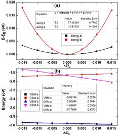
Figure 4. The total energy shift E–E0 (a) and the energy shift of the band edge position (b) as a function of lattice deformation  along a and b directions of α-CS.
Download figure:
Standard image High-resolution imageAs mentioned above, the difference between the C–S bond strength in armchair and zigzag directions will lead to anisotropic features of the 2D elastic modulus and the deformation-potential constant. As shown in figure 4(b), E1 is more insensitive to the strain along a (armchair) than that along b (zigzag) direction. In addition, the effective mass of holes evidently depends on the direction (table 2). The above results can be understood from the charge density of VBM (figure 3(d)). The range of charge delocalization along the armchair direction is wider compared with that along the zigzag direction, indicating that the effective mass of holes along the armchair direction is much smaller than that along the zigzag direction. In contrast, the effective mass of electrons shows a rather weak direction-dependence. This result can be well explained by the CBM exhibiting both covalent bonds and anti-bonds along the armchair and zigzag directions (figure 3(c)). Thus, the effective masses of electrons along the armchair (0.38 m0) and zigzag (0.32 m0) direction are approximately equal.
The predicted carrier mobility of α-CS shows an anisotropic characteristic (table 2). The hole and electron mobilities along the armchair direction are 1580.41 cm2 V−1 s−1 and 8453.19 cm2 V−1 s−1, respectively, about three times higher than that along the zigzag direction (436.87 and 3034.46 cm2 V−1 s−1), suggesting that the armchair direction is more favorable for the carrier conduction. The carrier mobility of α-CS is much higher than those of monolayer MoS2 (~60–200 cm2 V−1 s−1) [51]. The high carrier mobility and large difference in hole/electron mobilities will efficiently help migrate and separate photo-generated carriers. The main reasons for the high hole mobility of α-CS are discussed in the following aspects. On the one hand, the valence band along the Γ–Z path (armchair direction) is more dispersive than the conduction band (figure 3(a)), resulting in the larger (smaller) effective mass of electron (hole) of 0.38 m0 (0.23 m0). Therefore, the high hole mobility along the armchair direction benefits from the smaller effective mass of hole. On the other hand, for the case of the zigzag direction, the effective mass of electron is smaller than that of hole, but the deformation potential E1 of the CBM is greatly larger than that of the VBM. The CBM is mainly contributed from the delocalized states of C and S atoms, while VBM is partially contributed from the localized states of C atoms (figures 3(c) and (d)). Therefore, the E1 of the CBM is more sensitive to strain compared with that of the VBM along the zigzag direction, resulting in the large difference of E1 between CBM (−9.78 eV) and VBM (−1.69 eV), where the latter leads to the high hole mobility. Therefore, the high hole mobility attributes to the small effective mass and deformation potential.
3.4. Effects of strain on the band structures
Applying external strain is a common way to tune the band structures of 2D materials. We have performed calculations on the relation between the band gap and strain for α-CS (figure 5(a)). In the b direction, the band gap exhibits a linear decrease under tensile strain and then drops to zero when tensile strain is up to +0.15. In addition, the band gap decreases and arrives at zero at compressive strain of −0.18. When the a-direction strain is applied, the band gap monotonically decreases with increasing the tensile strain and becomes zero at +0.22. However, for compressive strain, the band gap is initially increased up to the maximal value (1.16 eV) at −0.03 and then decreases linearly with further increased compression. As shown in figure 5(b), the D0 along the a direction is more sensitive to the strain than that along the b direction, which agrees with the analysis of the in-plane stiffnesses. In addition, for the a direction, the strength of C1–S1 bonds gradually weakens with increasing the compressive and tensile strain, while the strength of C1–S2 bonds enhances (weakens) under the compressive (tensile) strain. In the case of b direction, the strength of C1–S1 bonds can be enhanced (weakened) by increasing the compressive (tensile) strain. In addition, the strength of C1–S2 bonds can be enhanced from partially covalent/ionic bonds to covalent bonds, by increasing the tensile strain along the b direction.
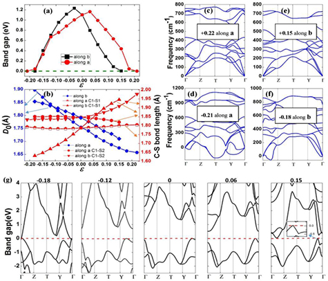
Figure 5. The band gap (a), buckling constant, and C–S bond length (b) along the a (b) direction as a function of strain. The strain is defined by ε = (L–L0)/L0, where L and L0 represent the strained and the pristine lattice parameters, respectively. Band gaps are presented by PBE functional. (c)–(f) The phonon spectra under the certain strains. (g) The band structures under different uniaxial strains along the b direction.
Download figure:
Standard image High-resolution imageTo shed more lights on the effect of band gap with strain, we calculate the band structures of α-CS at different uniaxial strains along the b direction (shown in figure 5(g)). The CBM shifts downward with increasing the stain strength and crosses the Fermi level at ε = -0.18. On the other hand, at ε = +0.15, α-CS also experiences a transition from semiconductor to metal due to its VBM crossing the Fermi level. Its CBM (2p states of C atoms) moves downward and away from the Γ point to a near k point locating on the Γ–Z path. The strength of C1–S1 bond weakens greatly along the zigzag (b) direction at ε = +0.15, resulting in the charge density around CBM (the charge density around CBM not shown) favouring the armchair (a) direction. The corresponding position of CBM transfers from Γ point to a point between Γ and Z (armchair direction).
To check the stability of the strain induced system, we calculate the phonon spectra under these certain strains. As shown in figures 5(c)–(f), α-CS will be stable with the axial tensile strain of +0.15 in the b direction and +0.22 in the a direction. For the compressive strain of –0.18 along the a (b) direction, α-CS has apparent imaginary frequencies of the acoustic phonon branch. However, α-CS is still dynamical stable with the compressive strain of −0.12 in the a (b) direction. Therefore, the band gap of α-CS can be flexibly modulated through the applied strain in a relatively wide range, which may be useful for applications in nanoelectronic devices.
3.5. Effects of the electric field (E-field) on the band structures
Very recently, many theoretical and experimental works have demonstrated that applying external E-field can efficiently modify the electronic structures of 2D materials [52–54]. We then explore the relationship of the band gap of α-CS with the perpendicular E-field. As shown in figure 6(a), the band gap does not depend on the E-field until 5 V Å−1. However, the band gap sharply decreases with further increase of the E-field. Specially, when the E-field is up to 0.75 V Å−1, the band gap closes. As shown in figure 6(b), the D0 and C–S bond lengths decrease only 0.12% compared with those of the pristine α-CS, indicating that the geometry of α-CS is insensitive to E-field. To explore the stability of this structure at 0.75 V Å−1, we also calculate the corresponding phonon spectra (figure 6(c)). It is stable with well separated positive acoustical and optical frequencies.
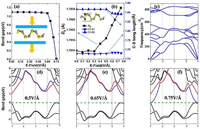
Figure 6. The band gap (a), the buckling distance D0 and the bond length of C1–S1 (C1–S2) (b) as a function of the electric field. (c) The phonon dispersion of α-CS under 0.75 V Å−1. (d)–(f) The band structures under the certain E-field. The blue (red) lines represent the conduction bands composed by S-3p (C-2p) states.
Download figure:
Standard image High-resolution imageTo better understand this phenomenon, the band structures of α-CS with different E-fields are calculated (figures 6(d)–(f)). The position of VBM is almost the same (with respect to the Fermi level), while the CBM moves downward with increasing the E-field and then crosses the Fermi level at the E-field of 0.75 V Å−1. As presented in figure 6(d), the conduction bands (C-2p and S-3p states) near the Fermi level are split (locating at Γ–Z and Γ–Y path) and partly degenerate (locating on Z–T–Y path). With respect to the C 2p orbital energy, the 3p orbital energy of S atom is higher. Thus, the S-3p orbitals are obviously affected under the perpendicular E-field in comparison with the C-2p orbitals. Therefore, the splitting of corresponding CB (blue bands composed by S-3p states) is further enhanced with increasing the E-field strength. Correspondingly, this certain band moves downward to the Fermi level (figures 6(e) and (f)). In contrast, the CB (red bands composed by C-2p states) is insensitive to the E-field.
3.6. Bilayer structures
For the α-CS bilayer, we design six possible stacking conformations, namely, AA-, AA'-, AB-, AB'-, AC-, and AC'-stacking (figure S2). The layer-to-layer space of six stacking patterns differs slightly ranging from 3.09 Å (AC-) to 3.47 Å (AA'-). Furthermore, the phonon dispersion calculations confirm that these bilayers are kinetically stable (figure 7). The AC'-stacking is the most favorable conformation for all the bilayer α-CS. The calculated band gaps (at the HSE06 level) of bilayers range from 1.60 to 1.92 eV, which are all smaller than that of single-layer α-CS (1.96 eV). As shown in figure 7, the feature of indirect band gap for bilayer α-CS is retained regardless of the stacking pattern. According to the band structures of six stacking patterns, the VBM locates on Γ point, while the CBM lies on the Γ–Z path. The positions of VBM with respect to the Fermi level are almost the same, while the CBM of the AB'- and AC-stacked bilayers are shifted upward compared with those of the AA-, AA'-, AB-, and AC'-stacked bilayers. To get more insights into the difference of the CBM, we further calculate the charge density corresponding with the CBM and VBM of six stacking patterns (figure 7). The VBM is contributed from delocalized states of the C atoms, while the CBM is mainly contributed from localized states of C and S atoms. Moreover, the wavefunction overlap indicates that weak 'quasi-bonds' exist in the interlayer regions, which results in the decrease of the band gap from monolayer to bilayer. Therefore, different stacking patterns play significant roles in electronic structures of bilayers.
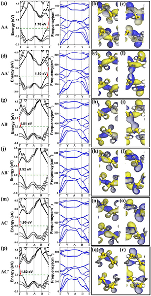
Figure 7. The band structures and phonon spectra of the AA- (a), AA'- (d), AB- (g), AB'- (j), AC- (m), and AC'- (p) stacking orders. The calculated band structures of six bilayers patterns at the HSE06 level. The VBM ((b), (e), (h), (k), (n) and (q)) and CBM ((c), (f), (i), (l), (o) and (r)) of the AA-, AA'-, AB-, AB'-, AC-, and AC'- stacking orders at the Γ point. The value of isosurfaces is 0.04 e Å−3.
Download figure:
Standard image High-resolution image3.7. The possible substrate for epitaxy growth
We further explore a suitable substrate for the α-CS growth. Graphite is usually used as a kind of common substrate for the nanoscale-material growth [55–57]. We choose the graphite (0 0 1) surface because its lattice constants are close to those of α-CS. The unit cell of heterostructure is composed by 2 × 2 unit cells for both monolayer α-CS and four graphite layers (figure 8(a)). The average values of the two separate lattice parameters of the new heterostructure are a = b = 4.90 Å, which are chosen to be the co-periodic lattice parameters. A lattice mismatch (δ) exists in heterostructure, which defined by this formula: δ = [(a1 – a2)/a2] × 100%. The a1 and a2 represent the lattice constants of monolayer α-CS on the graphite (0 0 1) surface and individual α-CS monolayer, respectively. The lattice mismatch is only 0.03% for our system. The optimum space (3.50 Å) between monolayer α-CS and graphite layers is slightly larger than that of the graphite (3.40 Å).

Figure 8. (a) The configuration of monolayer α-CS on the graphite (0 0 1) surface with four layers. (b) The density of states projected on the free-standing α-CS (red dashed) and α-CS on the graphite substrate (blue solid).
Download figure:
Standard image High-resolution imageWe next calculate the binding energy of α-CS + graphite heterostructure. It can be defined as: Eb = Etotal − Egraphite − Eα-CS. The Etotal, Egraphite, and Eα-CS are the energies of the composites, graphite substrate, and α-CS, respectively. The Eb is −40.28 meV, which is comparable to that of SiGe/BN heterostructure (−65.2 meV) [58], indicating that α-CS is more easily exfoliated from the substrate surface. Importantly, the DOS of α-CS has not been affected by the graphite substrate, where the most attractive electronic properties are well preserved (figure 8(b)). Therefore, it is possible for the α-CS grown on the graphite substrate.
3.8. Photocatalytic and optical properties
The appropriate band edge positions for straddling the water redox potentials are fundamental. It is noted that the water redox potentials depend on the pH value of medium [59–61]. Figure 9(a) shows the band edges of VBM and CBM (with respect to the vacuum level) for monolayer and bilayer α-CS compared with the water redox potentials at pH = 0 and pH = 7. For monolayer α-CS, the band alignments can straddle the water redox potentials at pH = 7. Although the α-CS is not suitable as an intrinsic photocatalyst in a pH = 0 solution, its VBM energy (−5.42 eV) is very close to the oxidation potential of H2O/O2 (−5.76 eV). To precede the water splitting, the small bias potential should be required of 0.34 eV. Notably, the CBM energy of α-CS (−3.37 eV) is much higher than the reduction potential of H+/H2 (−4.44 eV), suggesting that the force of driving water reduction reaction is strong. On the other hand, for all α-CS bilayers, the band edges of VBM and CBM are suitable for photocatalysis at pH = 7. Moreover, the band alignments of AB- and AB'- stacking bilayers locate at favorable positions for water splitting at pH = 0, which implies that different stacking orders can efficiently adjust the band edge of α-CS.

Figure 9. (a) The band edge positions of monolayer and bilayer α-CS calculated by HSE06 functional. The dot and dashed lines represent the water redox potential at pH = 0 and pH = 7, respectively. (b) The absorption coefficient of monolayer α-CS at the HSE06 level. The black solid and red dashed line are parallel (//) and perpendicular (⊥) directions, respectively.
Download figure:
Standard image High-resolution imageWe also investigate the light harvesting performance of α-CS by calculating the absorption coefficient in- and out-of-plane with the HSE06 functional, as shown in figure 9(b). The out-of-plane and in-plane absorption coefficient correspond to the polarization vectors perpendicular and parallel to the surface of α-CS, respectively. The prominent peaks of absorption coefficients occur at ~150 nm, and the highest value is up to 105 cm−1, suggesting that α-CS displays strong absorption strength in the ultraviolet region. Notably, the in-plane absorption coefficient is larger than that of the out-of-plane at the range of 200–800 nm, suggesting that the parallel polarized light exhibits stronger harvest ability in the ultraviolet and visible light regions. Thus, monolayer α-CS has a potential application in optical and photo-electronic devices.
3.9. The properties of water adsorbed on α-CS
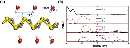
Apart from the structural stability of α-CS in implicit water at room temperature (figure 2(d)), we have also explored the properties of water adsorbed on α-CS. The double-side adsorption of 6 water molecules on the 3 × 3 supercell of α-CS is employed (figure 10(a)). The optimum space between water molecules and α-CS is about 1.74 Å, and the structural integrity of α-CS is not destroyed. The H–O bond length (H–O–H bond angle) of adsorbed H2O increases 0.02 Å (~2°) in comparison with that of the isolated water molecule, showing a small structural change during the whole adsorption process. The water adsorption energy of 0.37 eV is slightly higher than that of monolayer MoS2 (0.23 eV) [62], suggesting the adsorption energy lying between the physisorbed and chemisorbed states. Here, we present further discussions on the PDOS of the H2O + α-CS system (figure 10(b)). Clearly, the H-s (O-p) and C-sp (S-p) orbitals are hybridized in the energy range from −2 to −1 eV. The Hirshfeld charge analysis shows that each water molecule obtains 0.1 e from α-CS. Therefore, monolayer α-CS could be favorable for water adsorption.
Figure 10. (a) The side view of water molecules adsorbed on α-CS. White and red balls represent H and O atoms, respectively. (b) The PDOS of water adsorbed on α-CS.
Download figure:
Standard image High-resolution image
4. Conclusions
In summary, we theoretically investigate the structural, electronic and optical properties of α-CS based on the density functional theory. After confirming the thermal and dynamical stabilities, it can remain stable in liquid water at room temperature. Notably, the α-CS possesses a suitable band gap responding to the visible and ultraviolet light. The band edge positions of monolayer and bilayer α-CS in pH neutral water satisfy the criteria for perfect photocatalysts. In addition, the large difference of hole and electron mobility can facilitate the migration and separation of carriers. Hence, α-CS could be a good candidate as a potential photocatalyst. Recently, 2D SnS nanoplates have been synthesized on the freshly cleaved mica substrate [63]. Here the graphite surface is predicted to be an available substrate for the α-CS growth. We hope our results can stimulate future theoretical and experimental works on 2D group IV–VI monolayers as metal-free photocatalysts.
Acknowledgments
This work is supported by the Jiangsu Specially Appointed Professor Plan, the National Natural Science Foundation of China (Grant No. 11704198), the Natural Science Foundation of Jiangsu Province (Grant Nos. BK20141421 and BK20150826), and the Scientific Research Foundation of Nanjing University of Posts and Telecommunications (Grant Nos. NY215035 and NY217038).
Supporting information
The structures of monolayer CS and bilayer α-CS (stacks.iop.org/JPhysCM/30/065701/mmedia).