
Abstract
Direct characterization of planar atomic or molecular scale devices and circuits on a supporting surface by multi-probe measurements requires unprecedented stability of single atom contacts and manipulation of scanning probes over large, nanometer scale area with atomic precision. In this work, we describe the full methodology behind atomically defined two-probe scanning tunneling microscopy (STM) experiments performed on a model system: dangling bond dimer wire supported on a hydrogenated germanium (0 0 1) surface. We show that 70 nm long atomic wire can be simultaneously approached by two independent STM scanners with exact probe to probe distance reaching down to 30 nm. This allows direct wire characterization by two-probe I–V characteristics at distances below 50 nm. Our technical results presented in this work open a new area for multi-probe research, which can be now performed with precision so far accessible only by single-probe scanning probe microscopy (SPM) experiments.
Export citation and abstract BibTeX RIS

Original content from this work may be used under the terms of the Creative Commons Attribution 3.0 licence. Any further distribution of this work must maintain attribution to the author(s) and the title of the work, journal citation and DOI.
1. Introduction
Understanding of electronic and transport properties of atomic and molecular nanostructures is an essential step towards their utilization in any potential future electronic device [1, 2]. Therefore, different local-probe techniques of measurements addressing this problem have been proposed and extensively developed during the last 25 years [3–28].
These ultra-high vacuum (UHV) techniques could be easily divided into two classes according to the experimental geometry used. The vertical one is based on the break junction geometry [29] and single-probe scanning probe microscopy (SPM) techniques [30, 31]. Particularly, due to the unprecedented precision in a scanning tunneling microscopy (STM)-based methods, formation of a well-defined junction between probe and a single atom [32] or a molecule can be easily realized [31]. Therefore this type of experiments have provided significant input to fundamental understanding of single atom [3, 12, 17, 22] and/or molecule conductance [5, 6, 9, 12, 13, 22, 26]. However, mainly due to the limited number of atomic scale probes available in a single tip vertical geometry, the practical realization of novel electronic atomic scale devices requires now well prepared surface support and planar geometry for at least two interconnects.
For determination of the planar surface electronic and transport properties at the nanoscale mainly multi-probe SPM experiments have been considered [33, 34]. To date and up to our best knowledge the multi-probe state-of-the-art measurements of surface electronic and transport properties have been performed with probe separation distances up to the range of tens of nm and with no atomic-scale precision of probe contact position. Nevertheless, with standard 2-probe [8, 15, 16, 23, 27] or 4-probe [4, 7, 11, 18, 20, 23–25] methods of measurements characterization of a wide range of fundamental surface electronic properties has been realized. This includes, but is not only limited to understanding of: surface conductance channels [4, 18, 20, 24, 25, 35], surface conductance anisotropy [7, 24] or surface electronic bang-gap [16]. These standard multi-probe methods have been also applied to determine conductance of self-assembled molecular structures [11] or transport properties of graphene nano-constrains [23, 27]. Moreover, by combination of multi-probe methods with a high-resolution STM experiment Qin et al have showed how the local atomic environment affects transport properties of atomic wires [15]. Alternative multi-probe based technique determining the local surface conductivity with lateral resolution reaching about 1 nm or less is based on a 3-probe experimental setup [28]. In the so-called scanning tunneling potentiometry (STP) two external probes serve as current suppliers and the third, central probe, operates in STM mode and measures the local potential with respect to some external ground or a tip. In this approach the local electrochemical potential can be determined, which is furthermore applied to calculate the local surface conductivity [10, 19, 21, 28]. Since the internal probe can operate almost with the same resolution as in the single probe SPM experiments, this technique can give information about conductance of nanoscale systems, like e.g. a single step edge on a surface [10, 19].
However, to directly characterize the atomic or molecular nanoscale systems on a surface, one has to considerably reduce the distance between the current supplier probes. Moreover, the planar transport measurements on atomic level requires unprecedented stability of atom contacts and manipulation of the scanning probes with real relative atomic precision. Solving the above challenges meets many technical obstacles, which have to be overcome [36]. In this work, we show that the planar multi-probe experimental methods can reach the atomic precision of the vertical geometry experiments, which are based on the STM junction. This is realized by describing our full experimental methodology of the two-probe STM experiment performed on a model atomic-scale system: dangling bond (DB) dimer wire supported on a hydrogenated (0 0 1) surface of germanium.
Dangling bond (DB) wires formed by STM tip induced hydrogen atom desorption from hydrogenated semiconductor (0 0 1) surfaces of silicon or germanium are candidates for atomic-scale interconnects [37–39] addressing atomic [40–45] or molecular [46, 47] quantum electronic devices. The transport properties of DB wires were subjected to numerous theoretical modeling studies [37–39, 48–51], however any direct experimental characterization of these properties have not been reported.
The article has the following structure. We start from a detailed description of experimental methods. Then we show two STM tip coarse approach to the Ge(0 0 1):H surface, which is followed by two-probe STM experiment performed on probe to probe distances below 2 µm. Application of our two strategies of STM-based desorption of hydrogen atoms from Ge(0 0 1):H surface results in formation of 70 nm long DB dimer wire. This structure acts then as a label proving that our STM approach methodology provides a surface-defined and atomically precise orientation between lateral positions of two STM tips. Finally we present our two-probe spectroscopic results obtained on the DB dimer atomic wire, which include vertical contact description strategies and I–V characteristics performed on two atomically defined probe to probe distances.
2. Methods
The experiments were carried out in the recently assembled UHV system equipped with the ScientaOmicron low-temperature 4-probe STM (LT-Nanoprobe) at the Jagiellonian University in Krakow. The 4-probe STM stage is located in a bath cryostat under a high resolution scanning electron microscope (SEM) Gemini Column (Carl Zeiss). The detailed description of the LT-Nanoprobe 4-probe STM machine performance can be found in the work by Jang et al [52]. In current work, the two-probe experiments were carried out at cryogenic temperature of around 4.5 K (liquid helium, LHe) with electrochemically etched tungsten tips used as probes. For the purpose of multi-probe experiments we optimized our tungsten wire etching procedure by application of short cut-off times (below 500 ns) resulting in preparation of mechanically stable tips with diameters below 50 nm.
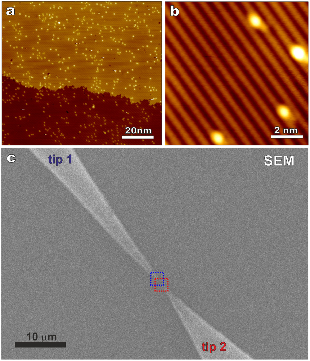
For this study the 4-probe STM chamber was attached to a preparation chamber equipped with a sample stage enabling direct current heating, a noble gas ion gun, home built hydrogen cracker and an infrared pyrometer. Both parts of the UHV system have base pressure below 1 × 10⁻¹⁰ mbar. To prepare a hydrogenated Ge(0 0 1):H surface, we followed the standard protocol described elsewhere [53]. We used 2 × 10 mm2 samples (germanium wafer, TBL Kelpin Crystals, 0.5 mm thickness, undoped) mounted on a direct heating holder. After introduction into UHV condition, the samples were first outgassed for 8 h at 500 K. Then, we annealed the samples by direct current heating at 800 K until the pressure in the preparation chamber did not exceed a low 10−10 mbar level. The main part of sample preparation protocol consisted of cycles of 1 keV Ar+ sputtering for 15 min with the sample kept at 1040 K. The preparation of hydrogenated Ge(0 0 1):H surfaces was performed by exposure of bare Ge(0 0 1) surface to atomic hydrogen formed by a precisely dosed H2 flux coming through the hot tungsten filament. During hydrogen passivation procedure the sample was kept at 485 K and the hydrogen partial pressure in the UHV chamber was maintained at 1 × 10⁻⁷ mbar. The above routine results in hydrogenated Ge(0 0 1):H surface with monohydride (2 × 1) reconstruction consisting of germanium dimer rows with each surface Ge atom possessing one H atom attached as confirmed by STM images (figure 1). Defects observed as protrusions on atomically flat terraces are mostly in the form of native bare Ge atoms possessing DBs. Particularly on the high resolution STM image in figure 1(b) four bright features correspond to one single bare Ge atom and three bare Ge dimers.

Figure 1. STM and SEM images of hydrogenated Ge(0 0 1):H surface after UHV preparation procedure performed in LT-Nanoprobe system. (a) STM image, 20 pA, −2 V. (b) STM image, 50 pA, −0.5 V. (c) SEM image (5 keV, 20 pA) of two tungsten tips approached to Ge(0 0 1):H surface. Both tips have a diameters below 50 nm, what also enables two-probe experiments on probe to probe distances below 50 nm. Note that Ge(0 0 1):H surface has no micrometer scale defects. Dotted squares show overlap of scan ranges for both STM scanners used in the experiment.
Download figure:
Standard image High-resolution image3. Results and discussion
3.1. Coarse approach and fine STM-based probe to probe positioning
Two-probe STM experiment starts with a coarse positioning of STM probes. The tips approach a Ge(0 0 1):H surface at about 2 µm of a lateral separation distance between them. This value is related to 2 × 2 µm2 fine piezo STM scanner range at LHe conditions. About 2 µm separation distance between probes is then enough for both scanning areas to overlap and it gives sufficient space for a two-probe experiment. This is presented in figure 1(c), where the corresponding STM scanning areas are marked by two dotted squares. During coarse positioning procedure the probes are navigated by the use of high resolution SEM Gemini column. Electron beam related carbon contaminations or vacancies created in the surface layer due to secondary electron induced desorption affect a germanium substrate atomic-scale quality. To reduce such destruction, we optimised the coarse positioning procedure and practically used the lowest available SEM current and relatively low energy (20 pA, 5 keV). After fine STM feedback loop based approaches of both tips, the SEM beam is switched off. Nevertheless, the SEM-based approach procedure affects the quality of Ge(0 0 1):H area underneath the tips. Due to this reason the tips are afterwards slightly retracted by a few hundreds of nanometres and the sample stage is moved laterally by a few microns to a region not exposed to high dose of SEM electrons.
In the second step of our two-probe STM experiment, the relative position of two given STM tip apexes has to be determined. This can be achieved by finding a relation between STM images of the Ge(0 0 1):H surface obtained with two different tips. The first solution is to use a natural morphology of surface terrace edges as the markers. This methodology was applied for previous two-probe experiments performed on Au(1 1 1) surface [52]. However, general morphology of terraces for a high quality, defect-free Ge(0 0 1):H surface is uniform on the scale of hundreds of nanometers. Finding a direct relation between two STM images of the same surface area is then not straightforward and it requires maintaining a high resolution of both STM tips measurements during large-scale imaging (hundreds of nanometers square areas). This technical step can last a few working hours and it significantly increases the time-scale of the whole experiment.
The second method for a direct determination of STM tip apex to apex relative position uses the artificially created markers. In case of the hydrogenated Ge(0 0 1):H, the markers can be easily formed by STM-based lithography. Indeed to construct such DB nano-patterns on Ge(0 0 1):H surface, there are two efficient protocols for atomically controlled STM tip induced H extraction on Ge(0 0 1):H surface at liquid helium temperature conditions. In both cases, the procedure starts from a perfectly hydrogenated Ge(0 0 1):H surface area. In the first protocol, the extraction is performed by pulsing the STM tip bias voltage with the STM feedback loop open [42, 53]. In this case, we approach the tip over the hydrogen dimer selected for extraction with the STM feedback loop parameters set on about I = 1 nA tunnelling current intensity and a V = −0.5 V bias voltage. The tip apex is positioned over the dimer according to the Ge(0 0 1):H filled-state STM image. Subsequently, the feedback loop is turned off and the desorption process starts with a voltage pulse set up to positive biases, higher than +1.5 V (the exact value depends on the exact STM tip apex and typically is not larger than +2 V). The procedure can be repeated step-by-step until the targeted DB dimer pattern is constructed. Note that here, unlike in the case of the Si(0 0 1):H surface [54], our STM voltage pulse protocol extracts a pair of H atoms per pulse instead of a single H. The above described protocol allows for the efficient construction of a predesigned DB dimer nanostructure with atomic precision [42, 53]. This precise H extraction method is, however, time-consuming and so it was limited to DB structures containing up to tens of DB dimers.
There is another method to improve the efficiency of DB structure formation. It uses the STM feedback loop to control the tunnelling current during the desorption process. In this case, the desorption is realized during continuous movement of STM tip along a defined path above the surface [55]. Starting again with perfectly hydrogenated surface, we place the STM tip above the centre of hydrogenated germanium dimer. Then, we change the STM feedback loop to conditions allowing very efficient H desorption. The exact STM parameters depend again on the particular STM tip apex. The tunnelling current typically is in the range of 2–3 nA and bias voltage is about +2.5 V. Then, we move the apex along surface dimer rows at a constant speed (~5 nm s−1). To reduce the possibility of drift induced errors in the resulting DB line, we do not extend again the pattern more than up to 10 nm. In most cases, the newly formed DB structure possess still some single H atoms, which can be then removed by the previously described protocol. Longer wire manufacturing requires a superposition of the several elementary steps of DB line formation.
Figure 2 presents the patterns of two and three DB wires on Ge(0 0 1):H, which were formed by the described closed feedback loop strategy with one of the two STM probes. The patterns were then characterized with the two different STM tips. Importantly, the same wires were imaged by the second STM tip, while the first STM tip was still simultaneously imaging the Ge(0 0 1):H surface in an atomically defined distance from the pattern. This was confirmed by (2 × 1) reconstruction of the Ge(0 0 1):H surface.
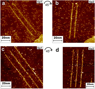
Figure 2. STM images (−2 V, 10 pA) of about 100 nm long DB wires formed on Ge(0 0 1):H surface in two separate experiments. Both patters were prepared with one STM tip by controlled desorption of H atoms ((a) and (c)) and then found and imaged with the second STM tip ((b) and (d)). Note that due to different real space orientation of STM scanners, images in (b) and (d) should be rotated by about 45 degrees with respect to images in a and c to directly see their correspondence.
Download figure:
Standard image High-resolution imageTo go a step forward and to confirm the above achievements in the two-probe experiment methodology, we have decided to form atomically 'perfect' pattern on Ge(0 0 1):H. The DB dimer wire presented in figure 3(a) is oriented along Ge(0 0 1):H reconstruction rows. It is formed by the closed feedback loop method followed by a few single and dimer atoms desorption with the open loop method. The length of the wire is about 70 nm. According to the dimensions of our tungsten tips observed by high resolution SEM (<50 nm each), it is an ideal candidate for atomic scale two-probe experiment. Please note that the preparation and detailed STM characterization of the wire were performed on eight small 15 × 15 nm2 STM scanning areas and the whole procedure took about five working hours. During this time and particularly during the STM-based hydrogen desorption experiments, the second STM tip was in the close vicinity of the used STM probe, only about few hundreds of nanometers apart. After the wire formation, the first probe was kept with its STM feedback loop closed at the one end of the structure, while the second STM tip was approached at the other end in the geometry presented schematically in figure 3(b). As already mentioned, both tungsten probes had stable apexes with diameters below 50 nm (figure 3(c)). The above described experiment proved also that the sharp apexes were maintained even after DB wire formation procedure. For the final test of the STM probe, to probe limits in the atomic-scale precise two-probe experiments, both tips were progressively approached along the wire in the STM scanning mode. This is shown on the insets in figure 3(d), where both simultaneously obtained STM images (−0.5 V, 50 pA) clearly show the atomic resolution on the wire. At the probe to probe distance of about 30 nm both tips interact directly with each other. This was observed as a sudden increase of STM constant current Z position, due to the STM feedback loops, which retracted both tips. Interestingly the tip apexes were preserved after such a controlled and soft tip to tip contact.
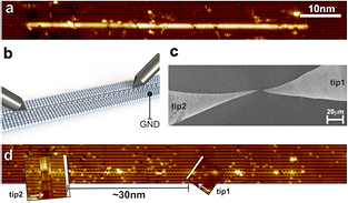
Figure 3. (a) STM image of a DB dimer wire on the Ge(0 0 1):H surface at 4.5 K (+1.0 V, 50 pA). The ~70 nm long wire consists of 156 bare Ge dimers (DB dimers) and has 14 atomic scale defects including 9 single Ge atoms (single DBs) and 5 unknown defects (adsorbates or vacancies). The structure is constructed by several line desorption procedures (STM feedback loop closed) followed by a few single hydrogen atoms desorption procedures (STM feedback loop open). (b) Schematic view of the two-probe experiment geometry. Both STM probes approach the same atomic-scale wire of bare Ge dimers along Ge(0 0 1):H reconstruction rows. (c) SEM image of two tungsten tips approached to Ge(0 0 1):H surface. Both tips have a diameters below 50 nm, what also enables two-probe experiments on probe to probe distances below 50 nm. (d) STM image of the same DB dimer wire as in (a) (−0.5 V, 50 pA). Insets: two STM images obtained simultaneously by two different tips in the geometry shown in (b) and (c). White arrows point the slow STM scan direction. White bars present on the insets are due to retraction of the tips after their contact on probe to probe distance of about 30 nm.
Download figure:
Standard image High-resolution image3.2. Contact determination
The results presented in figure 3 show that the relative lateral positions of two STM probes on Ge(0 0 1):H surface can be determined with unprecedented atomic precision. However, to perform multi-probe characterization of atomic-scale systems, one should also have the possibility to tune the electronic contacts between STM probes and the Ge(0 0 1):H surface with the same level of precision. The new ScientaOmicron LT-Nanoprobe 4-probe system used for this study has sub-Ångström stability in vertical probe positions without STM feedback loops and on the time scale of minutes [52]. This enables to precisely control contact resistances of each of the STM probes.
In general, analysis of atom to atom [32, 56] or atom to molecule [12, 31, 57] contacts is a complex problem and it has been studied by STM technique mainly on metal substrates. In case of metals, the absence of substrate band gap allows analysis of current (I) versus tip to sample distance (Z) for low biases of STM probe (V). As a result, the contact resistance/conductance can be determined. The use of a low bias voltage around the surface Fermi energy in those I(Z) experiments maintains the junction current on the relatively low values, allowing for preservation of the junction structure unaffected. These experiments particularly analyze in detail the passing between three different contact regimes: tunneling, electronic and mechanical contacts. In the case of surfaces with a band gap around the Fermi energy, such analysis is difficult to perform, because it is then required to use bias voltages larger than corresponding valence and conduction band edge of the corresponding surface. In general case, large bias voltages affect the interpretation of the measured contact conductance, since the corresponding I(V) plots deviate from the linear dependences due to the presence of some resonant states. Moreover, in the case of surfaces with a band-gap, tip-induced band bending (TIBB) effects are also present. Therefore, TIBB may strongly influence the different contact regimes.
Interestingly, the mentioned problems with semiconducting surfaces are not present in the case of Ge(0 0 1):H surface used in this study, where the valence band edge crosses the Fermi energy [58]. As a result, the surface band gap is located purely within the bulk empty states [53]. This Fermi level pining effect, which is specific for the Ge(0 0 1):H surface, facilitates a detailed analysis of STM tip to surface contact, which can be performed in a similar way as for metal substrates. The example of detailed analysis of contact between STM probe and hydrogenated Ge(0 0 1):H surface region is presented in figure 4(a). In contrast to the most typical I(Z) characterization of single atom contacts for one particularly chosen low bias voltage, we decided here to perform series of I(V) measurements on different tip to sample distances. This more sophisticated method of contact determination was applied here due to strongly non-linear I(V) dependences for Ge(0 0 1):H surface, which starts to deviate from a linear behavior for absolute values of voltages higher than 20 mV. Figure 4(a) shows a series of I(V) curves obtained for very low biases around Fermi energy over an hydrogenated dimer on Ge(0 0 1):H, which is located far from surface DBs. For distance of (Z0 − Z) = − 0.55 nm, we observe jumping increase in I–V slope, which is then followed by its saturation. This is also clearly seen in figure 4(b), which shows corresponding contact conductance presented in conductance quantum units as a function of tip to Ge:H hydrogenated dimer row relative distance. In this case, each conductance value is determined by linear regression fit to the data from figure 4(a). Please note that we obtained contact conductance saturation value on the level of 1 × 10⁻⁵ G0, what corresponds to about 1 GΩ junction resistance. Similar measurements were performed for contacts above DBs on Ge(0 0 1):H surface. In those cases the results were less repetitive, what is related to higher chemical activity of unsaturated Ge atoms and their possible dynamical behavior, i.e. Ge dimer switching between two equivalent geometries [55, 59]. These facts cause stronger dependence of the results on an exact tip apex structure and also the tip lateral position. However, in general case of DBs, we observe about two orders of magnitude decrease in contact resistances to values of about 10 MΩ (~1 × 10⁻³ G0). For a perfect DB dimer wire on Si(0 0 1):H or Ge(0 0 1):H we expect a one channel conductance [39] as for single metal atom chains [3, 57], which should give the values of G on the level of G0. In cases of both hydrogenated surfaces few orders of magnitude lower values of conductance for each of the tip to sample junction contacts may hinder determination of transport properties of DB wires around the Fermi level in a most straightforward two-probe experiment design, where both STM tips are in single atom contacts with DBs. One possible way to solve this problem is to change the two-probe DB wire characterization methodology. In this work, we have for example decided to keep one of STM probes in the tunneling junction regime with a high resistance in the order of tens of GΩ.

Figure 4. (a) and (b) Characterization of the contact between STM tip and the hydrogenated Ge(0 0 1):H surface. (a) I(V) curves around Fermi energy show linear dependence due to the Ge(0 0 1):H surface Fermi level pinning effect [58]. Starting from Z0(−0.5 V, 50 pA) the tip is progressively approached towards the hydrogenated Ge dimer, what decreases the junction resistance. For distances closer than −0.55 nm we observe saturation of the resistance at the value around R ~ 1.2 GΩ. Also for these small tip-sample distances switching behavior on our I–V dependences is clearly observed. (b) Conductance of the junction in G0 = 2e2/h units as a function of the tip to sample distance. The data are obtained from (a) by linear fitting procedures. We interpret the jumping decrease followed by saturation of the contact resistance in I–V(Z) dependences as a tunneling to contact regime crossover (dashed line). (c), (d) and (e) Two-probes characterization of DB dimer wire. (c) Presentation of the experiment design. Please see the text for details. (d) Two-probe current versus tip1 voltage curves obtained in two-probe experiments performed on two different distances (34.5 nm, green) and (48 nm, black). The presented spectra are representative from two sets of reproducible I–V dependences. The exact tip positions for the 34.5 nm experiment are marked by green and red circles on the upper panel. Inset: magnification of a dashed region. (e) Series of I–V dependences obtained for the two-probe experiment on DB dimer wire at distance of 34.5 nm. The green curve is presented in (d) as the representative one.
Download figure:
Standard image High-resolution image
3.3. Two-probe I–V spectroscopy on atomic wire
Formation of DBs by controlled hydrogen atom desorption introduces additional states in the electronic structure of hydrogenated semiconductor [41, 53, 54]. In the case of Ge(0 0 1):H surface dimer wire oriented along the reconstruction row corresponding π* states of DB dimers is characterized by a non- zero dispersive band within the band gap of Ge(0 0 1):H surface [53]. This band is located below the Ge conduction band edge and starts around +0.45 eV above the Ge:H Fermi level. Note that intuitively the dispersion of the bands must be larger in the direction parallel to a DB dimer wire than perpendicular. To probe the electronic transport through these states and along a DB dimer wire, we designed and performed the following two-probe STM experiment on the wire presented in figure 3. First, we have decided to keep one of the STM probes in the tunneling regime. It is our master (source) probe, which is marked as tip1 in figure 4(c). As the surface π* states of interest are located significantly above the Fermi level the tunneling regime allows us to tunnel with electrons having enough energy i.e. larger than 0.45 eV and also to control precisely current flowing through the system at the same time by adjusting the tip1—wire tunneling junction resistance. The second STM probe marked as tip2, is our slave (drain) probe. Tip2 is in a direct, single atom contact with the DB dimers forming the wire. The contact between this drain probe and DB dimer from the wire was established by approaching the tip2 towards the sample by Z-Z0 = −0.45 nm from Z0 distance determined by STM parameters −0.5 V and 50 pA. In this case, the resistance of the tip2—wire junction determined by the procedure discussed in the previous paragraph was about 25 MΩ. As shown in figure 4(c) in our two-probe experiment design, the sample is not connected to the ground. Obviously in this case and to avoid tip crash both STM feedback loops must be opened as well. To perform the two-probe characterization of the wire, we have grounded the slave STM probe (tip2), applied a bias voltage on the master probe (tip1) and measured the corresponding current intensity using the STM preamplifier of the tip1. Importantly, to keep the same notation as in the STM community, we still refer in this paragraph to bias voltages in reference to the sample, i.e. empty states are probed with a positive voltage. Please note that with a direct chemical contact between both STM probes and the DB dimers of the wire, the control over the current flowing through the system would not be possible. In this case, probing of transport through the electronic states located above +0.45 V with respect to the Fermi level would be extremely challenging due to resulting high current densities.
We have performed two-probe experiments for the tips located on the DB dimer wire in the positions marked in figure 4(c) by dots. First, the inter-tip distance was about 48 nm, which corresponds to exactly 120 DB dimers oriented along the Ge:H reconstruction row. In this case, on this DB dimer wire and between the 2 tips, there were 9 atomic-scale defects. The corresponding I(V1) dependence measured for this configuration is shown as a black curve in figure 4(d). As expected the current starts to increase at bias voltage threshold of about +0.45 eV (see the inset in figure 4(d)) and finally reaches about 100 pA for +1 V. Interestingly the monotonic I(V1) dependence drastically changes once we moved both probes closer to a distance of about 34.5 nm (green curve in figure 4(d)). In this second case, STM probes were separated by exactly 86 DB dimers forming an atomic wire with only 7 atomic-scale defects. Importantly, there is no difference between spectra for V1 voltages lower than +0.4 V (see the inset in figure 4(d)), what strongly supports the assumption that the local electronic structure of both tip to wire junctions is maintained in both experiments. In contrast, for energies above +0.4 eV, we have observed a general increase in the current flowing through the surface, which is also related to higher noise seen on the green spectra. These observations can be explained by both (1) smaller probe to probe distance and (2) the lower number of atomic defects on the wire between source and drain probes. Moreover, on the green I(V1) dependence, we have observed peaks for energies around +0.6 eV, +0.7 eV and +0.8 eV, which are reflected in three negative differential conductance regions present in the system for energies +0.65 eV, +0.75 eV and +0.9 eV. This non-trivial effect of non-monotonic current-voltage behavior is reproducible as presented in Figure 4(e). We propose the following interpretation of these data: in the peak regions, we observe the effective and resonant transport through the surface π* states along the whole system. In the negative differential conductance regions charge starts to be localized on some parts of the wire and effectively blocks the transport for these particular energies.
As here we were focused on the technical aspects of two-probe STM experiments, the detailed analysis of the presented two-probe I–V data, which needs further research including particularly theoretical modeling studies, is beyond this work.
4. Conclusions
The results described in this work show that we have established methodology for a fine relative positioning of two STM tips on a surface with unprecedented atomic precision and with a lateral probe to probe distance below 50 nm. Moreover, we performed two-probe spectroscopic experiments testing directly the electronic transport through model atomic-scale system: 70 nm long DB dimer wire fabricated on Ge(0 0 1):H surface by controlled hydrogen atom desorption. These results open the possibility of direct characterization of electronic transport properties on other atomic- and molecular-scale systems in a fully planar geometry by atomically precise two-probe STM experiments.
Acknowledgments
This work was supported by the FP7 FET-ICT 'planar atomic and molecular scale devices' (PAMS) project (funded by the European Commission under contract no. 610446). MK acknowledges financial support received from the Foundation for Polish Science (FNP). RZ acknowledges support received from KNOW (scholarship KNOW/59/SS/RZ/2016).