

Abstract
Surface acoustic waves, the microcosmic cousins of seismic waves, can be generated and precisely controlled on a microscopic scale by applying a periodic electrical signal to a piezoelectric substrate. Harnessing and exploring their interactions with two-dimensional van der Waals (vdW) systems opens new frontiers in materials science and engineering. As part of a special issue on these guided elastic waves for hybrid nano- and quantum technologies, our review highlights work focusing on acoustically-induced transport phenomena at low temperatures that arise from the interaction between the surface acoustic waves in a piezoelectric substrate and a vdW material on its surface. A main focus is on technological methods to control the carrier concentration in transport and strain-related effects that can act on the carrier motion as an effective magnetic field.
Export citation and abstract BibTeX RIS

Original content from this work may be used under the terms of the Creative Commons Attribution 4.0 license. Any further distribution of this work must maintain attribution to the author(s) and the title of the work, journal citation and DOI.
1. Introduction
Since the discovery of graphene, the family of van der Waals (vdW) materials has expanded remarkably and now covers the full spectrum of 'classical' solid state system properties, including superconducting, metallic, semiconducting, and insulating materials. Generally, vdW materials are characterized by strong covalent bonds between atoms within an atomic plane and much weaker interlayer vdW forces [1, 2]. This allows us to obtain truly two-dimensional (2D) single crystals with a thickness of only one atomic layer by breaking the interlayer bonds in the bulk materials and transferring isolated layers onto a substrate for further studies. The ability to pick up, stack and combine various 2D materials is key to build vdW heterostructures from base materials that possess either similar or very distinct electronic, optical, and magnetic properties. Specific 'magic' twist angles between stacked layers can even exhibit exotic physical characteristics that are normally alien to the materials [3, 4].
In this focused review, part of larger topical special issue on elastic waves, we will discuss transport studies of two exemplary vdW systems under the influence of mechanical strain waves called surface acoustic waves (SAW) that propagate through these materials. There exists many facets to the interaction between a SAW and a vdW material. Here, we will focus on acoustically-induced effects on the electrical transport that arise from the interaction between mobile carriers and the SAW, i.e. the acousto-electric interaction, and effects due to the deformation of the crystal lattice. We begin with a brief recapitulation and introduction of graphene, the first vdW material ever to be synthesized and studied, and MoS2 and their most relevant properties. We will then introduce the concept of acousto-electric transport, suitable gating technologies to control the carrier concentrations in a vdW material, and highlight some recent experiments. Finally, we will address the deformation of the crystal lattice that can result in artificial gauge fields and its impact on the transport in graphene and MoS2.
2. Graphene, MoS2, and the versatility of vdW materials
Research on two-dimensional electron systems (2DES) in AlGaAs/GaAs heterostructures using SAWs is well-established [5–15]. This III/V material platform offers both confinement for a 2D carrier system and a piezoelectric substrate for the SAW. However, all this work is limited to studying the electrical properties of a 2DES in a semiconducting (GaAs) material. Conversely, vdW materials can be exfoliated onto any piezoelectric substrate, enabling the study of a wide range of electrical properties by SAW. In the following, we will highlight in greater detail two vdW systems that possess semimetallic and semiconducting electrical properties and discuss their relevance for SAW studies.
The most prominent member of the vdW family is the semimetal graphene that can be synthesized by mechanically exfoliation from bulk graphite [16–18]. Monocrystalline graphene flakes synthesized in such an exfoliation process generally possess the highest achievable quality with mobilities exceeding  [19, 20]. However, the flake sizes and resulting stacks are limited to tens of micrometers. Graphene can also be synthesized on a larger scale by chemical vapor deposition (CVD) on catalytic substrates, such as copper or nickel [21–23]. Molecular beam epitaxial growth of graphene on SiC by sublimating Si from the SiC surface has also become established methods to synthesize larger graphene layers [24, 25]. However, a major drawback is the much lower carrier mobility due to disorder induced by grains and/or contamination.
Graphene is composed of a single layer of carbon atoms that undergo sp2-hybridization, involving one s-orbital and two p-orbitals. The hybridization gives rise to a hexagonal lattice structure with threefold rotation symmetry, as depicted in figure 1(a). The hexagonal lattice can be understood as the overlap of two distinct triangular sublattices A and B, with any two neighboring atoms belonging to different sublattices. The first Brillouin zone of the reciprocal lattice for graphene is presented in figure 1(a) as well. The reciprocal lattice also takes on a hexagonal shape, and owing to the presence of the two non-equivalent sublattices in real space, the corners of the hexagon correspond to two distinct points referred to as K- and K'-points in k-space [26–29].

Figure 1. (a) Monolayer graphene. Left: crystal lattice in real space with the two sublattices A in green and B in orange and lattice vectors  and
and  with a lattice constant of a = 1.42 Å: the nearest-neighbor vectors are indicated by
  , with i = 1, 2, 3. Along the x-direction, the edge is zigzag and along the y-direction the edge is of armchair type. Right: graphene lattice in momentum space with the low energy Dirac cones around K and K'. (b) Monolayer MoS2. Left/bottom: top view of the crystal lattice in real space and layer unit of a semiconductor 2H-MoS2 with each Mo atom located at the center of a trigonal prismatic cell and covalent bonds to six neighboring sulfur atoms. The small atoms represent S while the larger atom represent Mo. Right: electronic band structure of bilayer and monolayer MoS2, showing the transition from an indirect to a direct band gap. Band structure in figure (b) Reprinted (figure) with permission from [47], Copyright (2011) by the American Physical Society.
Download figure:
Standard image High-resolution imageGraphene is semimetallic due to the conduction and valence bands touching at the K and K' points in the Brillouin zone (zero-band gap), commonly referred to as Dirac points or charge neutrality points (CNP). Just like classical 2DESs confined to semiconductor heterostructures, for example, graphene's carrier concentration can be tuned via the application of a gate voltage. The missing band gap in graphene allows ambipolar control, i.e. the continuous transition of the Fermi level from the conduction band to the valence band. When the Fermi energy aligns with CNP, the energy where conduction and valence band meet, ideal graphene would become electrically neutral for  Kelvin. Real graphene can exhibit a small intrinsic band gap of approximately 42 µeV [30, 31] due weak spin–orbit interactions and which had been predicted to range between 1 µeV and 100 µeV [32–37]. The energy dispersion at the low energies around the CNP is linear, resembling the behavior of massless relativistic Dirac fermions. The presence of two sublattices in graphene introduces an additional degree of freedom called pseudospin, analogous to electronic spin. There exist additional important quantities called helicity and chirality related to the pseudospin operator's projection along the direction of motion. We will skip a detailed discussion at this point, suffice it to say that helicity and chirality are crucial for characterizing graphene's electronic properties and comprehending the behavior of its charge carriers [27, 30, 38].
Just like graphite, also bulk crystals of transition metal dichalcogenides (TMDCs) consist of monolayers held together by weak vdW forces. TMDCs of the type MX2 are composed of a transition metal element Mo, W, Nb or Ta denoted by M and two chalcogen atoms S, Se or Te, denoted by X2 [39, 40]. In contrast to the zero-gap semimetal graphene, TDMCs can have various band gap energies and cover material properties of semiconductors, metals and superconductors. In this review, we will focus on semiconducting 2H-MoS2, whose valley and spin degree of freedom makes it a potential candidate for applications in valleytronic and spintronic devices [41–43]
Monolayer MoS2, in its stable and natural 2H-phase, is a semiconductor, as depicted in figure 1(b), and consists of three atomic planes with the Mo plane (the transition metal element) sandwiched between S planes (the chalcogen) [44–48]. Semiconducting MoS2 crystallizes in a lattice with hexagonal symmetry ( ) and two layers per unit cell, hence the addendum '2H' [39]. Due to a quantum confinement effect on the electronic band structure, a transition from an indirect bulk band gap with 1.2 eV to a direct monolayer band gap of around 1.9 eV at K and K' has been observed [48]. In contrast to graphene, MoS2 has strong spin–orbit coupling originating from the d-orbitals of the heavy metal atoms and inversion symmetry breaking in odd layers. MoS2 promises a rich interaction between spin and valley physics such as a coexistence of valley-Hall and spin-Hall effects [46, 49–56]. vdW materials also have excellent mechanical strength [57–62]. The Young's modulus of graphene and MoS2 is
  and
and  , respectively. Monolayer graphene (MoS2) can withstand elastic stretch up to 25% (10%). These mechanical properties, the ability to pick up and transfer single layers and the extraordinary electrical properties are the motivation to study vdW systems through the interaction with time-dependent dynamic elastic sound waves, called SAW.
3. SAW and acousto-electric effects
SAW are periodic deformation waves that travel with the speed of sound along the surface of a piezoelectric medium. A common method to launch SAWs is based on the nanofabrication of interdigitated transducers (IDT), i.e. a signal converter that consists of a pair of interlocking metallic fingers [63, 64]. When a periodic electrical signal is applied, the inverse piezoelectric effect locally contracts and expands the piezoelectric substrate between the fingers, resulting in a directed acoustic phonon mode. The functional properties of an IDT, such as wave length or aperture, are dictated by the number, geometry and parallelism of the metallic fingers; interested readers may follow up on design rules in the manuscript by Mandal and Banerjee [64]. In the following, we will not delve into these details but highlight experiments that employed varying acoustic wave lengths. In the context of SAW, generally the Rayleigh mode is discussed that decays within one wave length away from the surface into the bulk. However, depending on the crystal direction, the material and its thickness, the IDT cannot only generate a pure Rayleigh surface mode, but also launch pseudo-surface waves that leak energy into the bulk or pure bulk modes.
The SAW propagation in a piezoelectric substrate is characterized by mechanical oscillations but also by a periodic electric field. This electric field acts on the mobile carriers in adjacent conductive materials, such as graphene, by affecting their dynamics and transporting them at acoustic velocities, thereby modulating the electronic properties. The coupling also efficiently transduces the kinetic energy of the SAW into the electronic system, causing an attenuation and energy loss of the SAW [14, 65, 66].
Hence, provided the surface adhesion is sufficiently strong and the vdW material conforms perfectly to the substrate deformation, two key contributions need to be considered when discussing the effects of a SAW: (1) the direct interaction of the piezoelectric field in the substrate with mobile carriers, and (2) a symmetry breaking of the crystal lattice and the ensuing effects on the band structure. In the following sections, we will discuss the direct interaction between the SAW and mobile carriers as well as gating technologies to control doping levels/carrier concentration. In section 4, we will address how strain-related effects modulate carrier dynamics through artificial gauge fields.
The propagation of a SAW through graphene films on a piezoelectric La3Ga5SiO14 substrate has been studied by high-resolution x-ray diffraction from a synchrotron radiation source to resolve the wave amplitude [67]. The topographs show that the presence of an graphene film insignificantly affects the SAW propagation. While there does not seem to be a sizable wave attenuation induced by the aforementioned coupling of the SAW's piezoelectric field with the mobile carriers in the graphene layers, kinetic energy is still transfered into the carrier system [5–15, 65, 68, 69]. The resulting experimental observations that arise from this interaction is dubbed 'acoustoelectric' (AE) effect [65]. A simple classical relaxation model can be used to derive the acoustically-induced current from the transfer of kinetic energy. In a closed electrical circuit, this AE current j is given by [14]:
where µ is the carrier mobility, Q is the phonon pressure, I the SAW intensity, and Γ the attenuation coefficient given by
The attenuation Γ is non-monotonic with the sheet conductivity  of a 2DES in a semiconductor heterostructure or a vdW layer, and will reach a maximum whenever
  matches with a characteristic conductivity,
  ,
,  for
for  . Here, ε and ε0 are the dielectric constant in the 2DES and vacuum, q the wave vector of acoustic waves and d the distance of the 2DES to the surface of the piezoelectric substrate that confines the SAW [70].
As we will discuss below, technologies exist to control the conductivity  through the carrier type and concentration (i.e. doping). In the semimetal graphene,
  can be widely tuned by applying a gate voltage. The tunability of the SAW properties and the doping level in graphene, along with the ensuing variable interaction, has also triggered considerable interest in theoretical research [71–74].
In the following sections, our discussion will primarily focus on measurements of the acoustic current j. However, we note that any current flow induces a (longitudinal) voltage drop along the current direction, which can alternatively be measured. When the system is additionally subjected to a perpendicular magnetic field, the motion of carriers is influenced by the Lorentz force perpendicular to the current direction, giving rise to more complex (magneto-)transport phenomena.
The first measurements of AE currents in graphene were experimentally reported by Miseikis et al [75]. The authors had wet-transferred CVD graphene on a bulk piezoelectric LiNbO3 substrate in a cutting direction of 128∘ Y-rotated between two IDTs, as shown in figure 2(c). Each IDT can either act as SAW emitter to launch a SAW or as a SAW receiver for the reconversion into an alternating radio frequency signal to analyze the phase and velocity changes and power losses.

Figure 2. (a) Top panel: relative SAW intensity versus frequency, measured by comparing the receiver and emitter IDT power. Bottom panel: dependence of the SAW-induced acoustoelectric current in the graphene layer with frequency for three absolute power levels at the emitter IDT. Reprinted from [78], with the permission of AIP Publishing. (b) Acoustoelectric current in a graphene nanoribbon as a function of SAW intensity at different frequencies . Reproduced from [76]. CC BY 4.0. (c) Configuration of SAW delay lines with graphene patterned between two IDTs to study the acoustoelectric effect in graphene. Reprinted from [75], with the permission of AIP Publishing.
Download figure:
Standard image High-resolution imageFigure 2((a), top) illustrates the dependence of the relative (SAW) amplitude as a function of the input frequency to the emitter IDT. The relative amplitude in units of decibels is a logarithmic scale to describe a ratio of the power level applied to the emitter IDT relative to the measured level at the receiver IDT. Figure 2((a), bottom) shows the directly measured acoustic current j in the graphene layer for three absolute power levels at the emitter IDTs, in (logarithmic) dBm. Figure 2(a) illustrates that frequencies covering the range of 12 MHz up to 480 MHz could be detected electrically in the graphene and also by a receiver IDT. Figure 2(b) show the linear dependence of j on the SAW intensity in a graphene nanoribbon (see equation (1)), here expressed in the linear scale units W/m, and estimated from the insertion loss of the applied power to the emitter IDT [76]. A similar emitter and receiver approach has been employed by Preciado et al [77] in a hybrid MoS2 on LiNbO3 device.
Considerable research efforts have been dedicated to studying the response of the AE current and the changes in the wave propagation in response to various stimuli, e.g. the SAW power, frequency, temperature or in combination with photo excitations in the vdW layer [72, 76–102].
When the charge carriers in a 2DES, such as in a vdW system or a classical semiconductor heterostructure, travel with a higher velocity than the acoustic wave, they can also transfer their kinetic energy to the wave instead of vice versa, contributing to an amplification of the SAW [103–107]. This has been observed in a graphene film on a surface of a Y-cut of lanthanum-gallium silicate Ga3TaGa3Si2O14 crystal, where carriers had been accelerated by applying a bias voltage to the graphene along the direction of the wave propagation [105]. This method also allows to attenuate the SAW by applying an inverse bias. Similar effects has been found in semiconductor materials on piezoelectric substrate [106, 107].
3.1. Dependence of AE transport on the charge density
Any conductive material in the path of a SAW, such as metallic films or a vdW layer, can affect the SAW propagation. The high conductivity of metals, which results in a strong SAW attenuation, is exploited in delay lines, for example [108]. The carrier concentration (and thus the conductivity) of many vdW materials can be controlled by gating and plays a critical role in the modulation of the SAW propagation and its interaction with mobile carriers. Hence, the variation of the charge carrier density is of significant importance for the exploration of AE transport phenomena. The field effect, typically employed to modulate carrier concentrations by a metallic gate electrode, must be separated from the SAW propagation, otherwise the SAW would experience a significant attenuation. This presents a technological challenge, as increasing the distance between a gate and a vdW material necessitates higher voltages for effective doping control. In GaAs-based devices, gating is accomplished either through a metallic top gate or a highly-doped GaAs layer grown beneath the 2DES. For vdW materials, on the other hand, new or adjusted gating solutions had to be developed. In the following, we will introduce these promising gating concepts.
There exist two primary techniques to induce changes in conductivity in a vdW material on top of a piezoelectric substrate: chemical doping and the application of a tunable gate voltage [80, 82–85, 88–90, 92, 93, 96, 109]. The investigation of chemical doping has revealed that the AE effect exhibits remarkable sensitivity in gas sensing and mass loading applications [84, 92, 96, 109]. Conversely, gating vdW materials is a more promising avenue for applications in transistors and quantum transport.
Achieving an effective and suitable gate configuration entails certain considerations. Firstly, it is advantageous to employ SAW with a high resonance frequency, as this allows for the use of a thin piezoelectric film as a dielectric layer between a vdW layer and the gate electrode. Conversely, obtaining a high-quality piezoelectric thin film has posed a significant technical challenge that researchers have been striving to overcome. In the following discussion, we will review various attempts made in this regard over the past few years.
Direct Back Gate: applying a gate voltage to an electrode on the back side of the substrate has been one of the most common methods for graphene on silicon dioxide substrate where a dielectric SiO2 with thickness d = 300 nm is on top of a low resistivity Si substrate that acts as a back gate electrode.
When attempting to observe AE currents in a vdW material on a piezoelectric substrate by electrostatic gating, it is crucial to exercise caution. Having a highly conductive metallic gate layer in close proximity to the piezoelectric substrate can lead to the attenuation of the SAW due to the aforementioned interaction with mobile carriers. For an efficient transfer of the SAW's kinetic energy into the vdW carrier system for electrical measurements, it is essential to position the gate layer at least one wavelength away from the substrate's surface. However, a large distance between gate and vdW layer, which converts to a small capacitance, renders gating difficult. Preciado et al have reported the use of an electrode on the back of a 500 µm LiNbO3 to tune the operation of a MoS2 field effect transistor [77]. The 'bulkiness' and large dielectric constant of the LiNbO3 piezoelectric of this sample make gating very ineffective. To achieve the same equalized electric field,  , from a back gate voltage of 10 V to graphene on a 300 nm SiO2, several hundred volts for the aforementioned LiNbO3 sample with 500 µm would be necessary.
Ionic Liquid Gate: in recent years, researchers have explored the application of ionic liquid gating to manipulate the electronic properties of vdW systems [110]. This technique involves depositing an ion gel onto a vdW material. The gel remains in a liquid state at room temperature and serves as a dielectric material with a high capacitance. When a gate voltage is applied, ions accumulate in successive layers near the material's surface, creating a nanocapacitor with a thickness of below 1 nm. The high capacitance results in significant electric fields and effective gating, as illustrated in figure 3(a).

Figure 3. Ionic liquid gating: (a) principle of ionic liquid gating, left: distribution of ions immediately after application of a gate voltage, right: equilibrium of ions distribution. The distance between ions and surface of the 2D material is about 1 nm. Reproduced from [110]. CC BY 4.0. (b) Sample schematic. The ion gel covers only the graphene in the center. The gate electrode is positioned out of the SAW propagating path. (c) DC resistance (top panel), SAW attenuation (second panel from top), phase shift of SAW (third panel) and AE current (bottom panel). (b) and (c) Reproduced from [83]. CC BY 4.0. All figures included under the Creative Commons CC BY licenses.
Download figure:
Standard image High-resolution imageThe charge accumulation or depletion of charge carriers in vdW systems depends on the polarity and magnitude of the applied voltage. Due to the immobilization of ions in the gel, SAW generated piezoelectric fields will not be affected and are capable of transporting charge carriers in the vdW materials [83, 89]. By applying a gate voltage to the ionic liquid, AE currents and voltages can be measured, with the polarization of the AE current changing when the CNP is crossed, as shown in figures 3(b) and (c).
While ionic liquid gating is a promising technique, there are challenges associated with it. It is difficult to be used at cryogenic temperatures for quantum applications because the gate voltage can only be varied in the liquid state of the ion gel. Additionally, special precautions must be taken to prevent the ion gel from coming into contact with the IDTs to avoid the generation of radio frequency induced charge carriers in graphene through the ionic liquid, which makes miniaturizing the device challenging.
Electrolyte-Gate: the application of a gate voltage to graphene submerged in an electrolyte solution has been explored, as depicted in figure 4. Ions within the solution migrate toward the material's surface, resulting in the generation of a substantial electric field. In this approach, the pH of the solution is determined by monitoring the alteration in acoustic-electric (AE) current in response to the electrolyte gate voltage [85, 92]. Similar to an ionic liquid gate, investigations at cryogenic temperatures are not feasible.

Figure 4. (a) Electrolytic gate setup. (b) AE current as a function of electrolyte gate voltage. (c) Application of AE current used in pH detection. Reprinted with permission from [92]. Copyright (2018) American Chemical Society.
Download figure:
Standard image High-resolution imageAlN: Liang and colleagues presented a novel device featuring a hybrid structure combining AlN SAW technology with a graphene field-effect transistor [88]. In this configuration, a piezoelectric AlN film is deposited onto a high-resistivity silicon substrate, and a molybdenum slab is patterned as a back gate on the same substrate. The AlN film serves a dual role as both the piezoelectric layer and the dielectric layer for the graphene field-effect transistor. Although the device demonstrated gate-tunable acoustic-electric current, it did not exhibit ambipolar behavior.
Flip Chip Gate: in a flip-chip configuration introduce by Lane et al, a graphene flake is exfoliated onto a SiO2/Si substrate for electrostatic gating. A separate piezoelectric LiNbO3 bulk substrate is then flipped upside-down and mechanically clamped onto a SiO2/Si substrate and separated by an air spacer of one SAW wavelength [90]. The small distance between piezoelectric substrate and graphene layer facilitates proximity coupling, i.e. it enables the AE effect, as originally described by Wixforth in 1989 [6]. It is important to note that the flip-chip scheme presents technological challenges due to the complexity and the difficulty in constructing such miniature devices.
Hybrid LNOI: recently, a novel hybrid device has been utilized to apply a back gate voltage to a graphene layer [98]. As illustrated in figure 5(a), this setup involves a CVD-grown graphene sheet placed on a 900 nm thick layer of LiNbO3, which in turn is situated on a 2 µm thick SiO2 insulating layer on top of a 500 µm thick p-doped silicon substrate. In this hybrid structure, the thickness of the dielectric layer has been reduced to approximately 2 µm, significantly lowering the required gate voltage compared to the conditions described in [77]. To prevent the SAW from being attenuated by the doped substrate, the SAW wavelength has been designed to be less than 2 µm, with the corresponding fundamental resonance occurring at around 2 GHz.

Figure 5. (a) Schematic of a piezoelectric hybrid LNOI. Upper panel: a back gate voltage is applied to the p-doped Si substrate. Lower panel: the wiring diagram for acoustic transport in graphene on top of the substrate. (b) Inset: acoustic current as a function of the frequency applied to the IDT, with a resonance/center frequency of approximately 1.88 GHz. Main panel: acoustic current as a function of power to the IDT with a fixed frequency of 1.88 GHz for various back gate voltages. The sign indicates the transition from electron to hole conductance. (c) acoustic current and Hall coefficients measured as a function of back gate voltage. All measurements were performed at 4.2 Kelvin. (a)–(c) Reprinted (figure) with permission from [98], Copyright (2022) by the American Physical Society. (d) Theoretical calculation of the longitudinal acoustic current based on the acoustogalvanic model from [111]. Reproduced from [111]. CC BY 4.0.
Download figure:
Standard image High-resolution imageFigures 5(b) and (c) demonstrate its versatility under cryogenic conditions and its accessible voltage range. By sweeping the back gate voltage,  , across the CNP around
  V, the AE current undergoes a sign change (figure 5(b)), indicating a transition of charge carriers transported by the SAW from holes (red) to electrons (blue).
The Hall coefficient is determined by measuring the Hall voltage when a magnetic field is applied and reflects the density of charge carriers. The gate dependence of the AE current replicates the characteristics of Hall coefficients around the CNP, as illustrated in figure 5(c), both of which provide insights into the charge density behavior of the graphene layer. The theoretical evaluation of the longitudinal acoustic current in figure 5(d) [111] qualitatively reproduces the experimental data. We note that in proximity to the CNP, electron–hole puddles are known to exist in disordered CVD graphene. Their formation contributes to competing AE signals originating from an approximately equal distribution of electrons and holes, which can broaden the CNP.
3.2. Graphene AE transport in an external magnetic field
For many decades, the influence of a magnetic field on AE effects had been studied in high-mobility 2DES GaAs heterostructures. In the presence of a magnetic field, the electronic energy levels and the density of states of a 2DES split into discrete Landau levels. This splitting is experimentally manifested by performing magneto-transport experiments that probe the oscillations in the longitudinal voltage and the (quantized) Hall effect in the transverse voltage [112] at cryogenic temperatures. Landau oscillations were directly observed by measuring the longitudinal AE current and voltage across a GaAs 2DES [5, 6, 12]. The interaction of SAWs within the quantum Hall regime in a high magnet fields revealed phase-shifts and an attenuation of the SAWs [5, 6]. Thus, the study of AE effects in the presence of a magnetic field is of paramount importance for the understanding of quantum effects and electron correlation phenomena.
Zhao et al reported the observation of Landau quantization through the oscillations of an acoustically-induced longitudinal voltage in CVD-graphene that had been transferred onto a piezoelectric GaAs substrate [95]. The authors found a SAW-induced phase shift within the quantum oscillations as shown in the upper panel of figure 6(a). The conductivity σxx
(green), which was measured in regular magneto-transport experiments, exhibits oscillations in B that indicate the Landau quantization of the density of states. Within each conductance minimum, a phase shift  of the SAW is observed that was determined by AE transport in the presence of B. This observation qualitatively agrees with SAW studies on GaAs 2DES [5, 6]. The center panel of figure 6(a) compares the
  to the acoustically-induced longitudinal voltage and the lower panel compares the conductivity σxx
with the acoustically-induced longitudinal voltage for the fundamental and the first two harmonics of the SAW in a smaller magnetic field range.
to the acoustically-induced longitudinal voltage and the lower panel compares the conductivity σxx
with the acoustically-induced longitudinal voltage for the fundamental and the first two harmonics of the SAW in a smaller magnetic field range.

Figure 6. Landau quantization probed by SAWs in (a) CVD-graphene on bulk GaAs at 4.2 Kelvin. Reprinted from [95], with the permission of AIP Publishing and (b) exfoliated graphene on LiNbO3 [99]. Left upper panel: the longitudinal conductivity σxx
(green) from regular magneto-transport exhibits Landau oscillations which are compared to the calculated SAW phase shift  (red). Left center panel: the longitudinal AE voltage (black) closely follows
  . Left lower panel: additional fine structure in the AE transport for various SAW frequencies. Upper right panel: SAW transmission and detected voltage as a function of the IDT frequency. Right center panel: quantum oscillations measured as the SAW phase shift by a detecting IDT for two exemplary gate voltages. Right bottom panel: Landau fan diagram constructed from various gate voltages. Reprinted (figure) with permission from [99], Copyright (2023) by the American Physical Society.
Download figure:
Standard image High-resolution imageThe additional fine structure in figure 6(a) can be attributed to commensurability [113] between the SAW wavelength and various defect sizes. Defects, including grain boundaries, wiggles and ripples, range in size from 1 µm to 10 µm and match the order of the acoustic wavelength. This can locally influence the conductivity and the SAW attenuation, where carriers may acquire geometrical phases that lead to quantum interference.
Fang et al have advanced the study of Landau quantization under the influence of SAW with exfoliated graphene transferred on bulk LiNbO3, which has higher piezoelectric coefficients. In their work, exfoliated graphene was encapsulated by hBN, and a graphite top gate was utilized to modulate the charge carrier concentration in the graphene sheet underneath. In this configuration, the phase shift of the SAWs qualitatively resembled the quantum oscillations observed in ordinary magneto-transport experiments. Figure 6(b) shows a Landau fan diagram of the SAW phase-shift, demonstrating a large spectrum of quantum oscillations. However, direct AE transport measurements, such as the observation of an AE current and voltage, were rendered impractical due to the screening effect of the graphite top gate on any in-situ electric fields induced by SAW in the graphene.
4. Artificial vector potentials in vdW systems
Graphene is not a perfectly flat 2D system. It is known to exhibit a natural rippling and corrugation [114–116] and certain steps in the sample fabrication can add folds and bends to a graphene flake. This local lattice deformation and the departure from flatness acts on the motion of the 2D Dirac electrons similar to an (inhomogeneous) effective magnetic field [117–137].
The energy of Dirac electrons in graphene is described in terms of a hopping probability between neighboring carbon atoms. In strained graphene, the distance between the atoms differs from that of a relaxed lattice, which directly affects this electron-hopping amplitude. This gives rise to an effective vector gauge potential, A, and a correction to the low energy Dirac Hamiltonian [27, 123, 124, 129, 132]. When graphene is rendered with a 2D strain field uij [132], the low energy Hamiltonian can be expressed as:

with  as the Pauli matrices. To preserve the time-reversal symmetry, the vector A has opposite signs at K and
  , i.e.
  , due to the presence of two sublattices in graphene.
  is the Grüneisen parameter representing phonon mode softening and hardening under tensile and compressive strain [138–140], t as the hopping parameter between the nearest neighbor atoms and a as the lattice constant of graphene crystal. Non-uniform strain is essential to generate an effective pseudo magnetic field, which is proportional to the derivative of A.
Apart from the natural deformation of graphene, due to its outstanding mechanical stability [57–60], large external stretch can be exploited to tune the hopping amplitude and generate artificial gauge fields A [131, 136, 141, 142]. First evidence of pseudo magnetic fields exceeding 300 Tesla have been found in scanning tunneling microscopy (STM) studies of graphene nanobubbles [119]. Around the bubble's apex, where the local deformation is strongest, the STM data revealed the presence of strong pseudo Landau level quantization. Enormous uniform pseudo magnetic fields have also been reported on a strongly deformed graphene flake in specially designed actuators that can induce a certain strain gradient [143–146]. Strain induced pseudo magnetic fields have also been present in artificial Dirac materials to form a graphene-like crystal structure [147].
Figure 7 visualizes the effects of uniaxial strain on graphene and the resulting pseudo magnetic fields. For an uniaxial stretch of 15 as shown in figure 7(a), the authors estimated a resulting pseudomagnetic field
  of up to 300 Tesla [143]. The calculated (local) density of states DOS in figure 7(b) illustrates that sufficient strain and the resulting pseudo magnetic fields can give rise to an energy quantization reminiscent of the Landau quantization in a large real magnetic field.

Figure 7. (a) For a graphene ribbon under uniaxial stretch (top), a uniform pseudomagnetic field  of several hundred of Teslas is estimated (bottom). (b) The calculated local density of states of both unstrained graphene and graphene under a constant strain gradient exhibit significant energetic splitting. Reprinted (figure) with permission from [143], Copyright (2015) by the American Physical Society.
Download figure:
Standard image High-resolution image5. SAW-induced gauge field effects in graphene
As previously discussed, a sufficiently large and well-defined static lattice deformation can lead to large effective pseudo magnetic fields and a quantization of the density of states. The time-dependent periodic deformation of a graphene sheet, induced by the propagation of a SAW has recently been identified to generate pseudo gauge fields in a more accessible way. In such a time-dependent periodic deformation, both pseudo magnetic and pseudo electric fields act on the carrier motion and give rise to novel acoustically-induced transport phenomena.
Two independent studies disclosed the existence of a SAW-induced pseudo gauge potential that contributes to a synthetic Hall response in the absence of an external magnetic field. Theoretically predicted by Bhalla et al and designated as acoustogalvanic (AG) effect as an acoustic analog of the photo galvanic effect [111], the phenomenon is connected to a Rayleigh mode. The simultaneous experimental demonstration and explanation by Zhao et al is based on an acoustic shear mode and will be outlined in the following [98].
The time-dependent deformation by a SAW will distort the graphene lattice and introduce a time-dependent pseudo gauge field [148] that will act on the motion of the Dirac fermions, resembling the effects induced by an ordinary electromagnetic field. Here, a Bleustein–Gulyaev (BG) mode, i.e. a shear mode of the SAW, will be considered, where the mechanical displacement of the carbon atoms is perpendicular to the SAW's propagation direction. We take equation (3) as the starting point and add the term  , which represents the piezoelectric potential from the substrate that is experienced by the nearby electrons in the graphene sheet. The vector potential
  will then be solved as follows:
where Δ is the hopping integral, εij
represents the components of the strain tensor and θ is the angle between the SAW propagation and graphene lattice coordinate. The threefold symmetry of the hexagonal graphene lattice contributes to 3θ. The corresponding pseudoelectric field,  , and pseudomagnetic field,
  , experienced by electrons are then given by
The parameter  is the angular frequency and u0 the wave amplitude. When static uniform strain is applied, the resulting local pseudo magnetic fields at the K- and
  -valley are of opposite sign and would cancel out. However, in the case of a time-dependent oscillating deformation that also induces a pseudo electric field, some of the vector components of
  and
and  survive. Their second order products provide non-vanishing contributions and can give rise to a transverse (synthetic Hall) potential.
A Lorenz-like transverse force, given by  , (
, ( means time averaging), will deflect the electrons and results in a build-up of charges. In a steady state condition, the force will be balanced by a transverse electric (Hall) field,

where  is the electron velocity under the influence of a pseudoelectric field
  . A SAW-induced synthetic Hall voltage will be formed that is given by
The value d represents the width of the graphene flake/Hall bar.
The classical Hall voltage of a 2DES in a real magnetic field solely depends on the carrier concentration. The formal expression for the SAW-induced transverse voltage in equation (7) is indeed reminiscent of the classical Hall effect. However, the resulting equation (8) depends on the carrier mobility and sample width. Hence, the SAW-induced transverse voltage must not be confused with a classical Hall effect originating from a pseudo magnetic and pseudo electric field that simply replace 'ordinary' fields. Rather, UH is the result of a transverse drag effect that is induced by the time-dependent pseudo gauge field.
The term  enforces a strong anisotropy for the observation of UH
. For unfavorable angles between the SAW and graphene's crystallographic direction, UH
will be completely suppressed. Using a diagrammatic approach, Bhalla et al has given a comprehensive explanation of the acoustic response to the sound-induced pseudogauge field in the absence of an external magnetic field [111]. Even though their discussion is based on Rayleigh modes, from the analysis of the interplay between transverse and longitudinal gauge field components, the author obtained a similar
enforces a strong anisotropy for the observation of UH
. For unfavorable angles between the SAW and graphene's crystallographic direction, UH
will be completely suppressed. Using a diagrammatic approach, Bhalla et al has given a comprehensive explanation of the acoustic response to the sound-induced pseudogauge field in the absence of an external magnetic field [111]. Even though their discussion is based on Rayleigh modes, from the analysis of the interplay between transverse and longitudinal gauge field components, the author obtained a similar  -dependence for their transverse AG effect. The calculated angular θ-dependence of longitudinal and transverse acoustic currents in their model is depicted in figure 8(b). While the longitudinal acoustic current is isotropic, the transverse acoustic current is highly anisotropic with respect to θ.

Figure 8. (a) Artistic illustration of a SAW propagation through a layer of graphene, showing the piezoelectric potential in the substrate and the wave through the graphene lattice. x0 and y0 indicate the graphene's crystallographic directions and x is the direction of propagation of the SAW [98]. (b) Calculated angle-dependence of longitudinal acoustic current (left) and transverse acoustic current (right) [111]. The transverse current exhibits a 6θ dependence. (c) Measured acoustically-induced transverse voltage as a function of the SAW intensity and back gate voltage at 4.2 Kelvin [98]. Both (b) and (c) are under the condition that no external magnetic field is applied. (d) Measured transverse (Hall) voltage for a superposition of an ordinary constant DC current and a SAW-induced current in an external magnetic field B at 4.2 Kelvin [98]. The variation of B and SAW power P allows to either compensate or amplify the transverse (Hall) voltage. Details in the main text. (a), (c) and (d) Reprinted (figure) with permission from [98], Copyright (2022) by the American Physical Society. (b) Reproduced from [111]. CC BY 4.0.
Download figure:
Standard image High-resolution imageFigure 8(c) shows measurements of a SAW-induced transverse voltage in monolayer graphene. To discriminate the aforementioned theory from actual experimental data, we will now refer to measured transverse voltages as Vxy . The data were collected on a graphene Hall bar of 30 µm width and 400 µm length. The graphene sheet was synthesized by CVD and directly wet-transfered to a substrate with a prepattered set of IDTs. The substrate is the specially tailored hybrid piezoelectric LNOI (LiNbO3 film on p-doped Si/SiO2) as discussed in section 3.1. It allows gating without damping the SAW by a nearby metallic gate electrode.
The measured acoustically-induced voltage Vxy
is of the order of ∼100 µV and thus consistent with the theoretically expected values when substituting the sample parameters into equation (8). Vxy
shows a dependence on the charge carrier concentration and type as well as the power of the radio frequency signal that is applied to the IDT. This power P parameterizes the SAW amplitude given by u0, and consequently, the amount of strain that is exterted on the graphene sheet. Figure 8(d) illustrates that a sufficiently large and fine-tuned SAW power can generate a 'synthetic Hall' voltage that completely compensates the real Hall voltage which appears in a large perpendicular magnetic field. The left panel of figure 8(d) compares  without SAW (blue curve) and with a fine-tuned SAW power (black curve). The right panel shows
  for six exemplary fixed magnetic fields. It illustrates that tuning the strength of the SAW allows to control the resulting Vxy
at a given magnetic field.
for six exemplary fixed magnetic fields. It illustrates that tuning the strength of the SAW allows to control the resulting Vxy
at a given magnetic field.
6. Recent frontiers: AE transport phenomena in TMDC
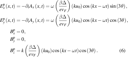
The generation and control of pseudo electromagnetic fields through the application of SAWs is also a viable approach to study other material platforms such as monolayer TMDCs or 3D Weyl semimetals [149], which possess symmetry properties similar to graphene. Rostami et al theoretically studied the effect of mechanical strain on the electronic structure of TMDCs, particularly emphasizing the low-energy aspects [150]. Unlike the typical Dirac-like Hamiltonian that is used to describe graphene, the contribution of the d-orbitals from the metal atom (M) and the p-orbitals from the chalcogen atom (X) (see section 2) lead to second-order effects from both momentum and strain. These terms not only introduce a single pseudo gauge field but multiple pseudo vector potentials, a characteristic that is absent in graphene. It is important to note that even when a real magnetic field is applied, these pseudo vector fields persist and cannot be nullified.
Kalameitsev et al predicted a novel valley AE effect in MoS2, a drag electric or spin current that arises due to a propagating SAW. Here, we will not delve into the complex details of this unconventional AE effect since higher order interactions are at play and so we restrict the introduction to a qualitative description. In a nutshell: the appearance of this valley AE effect is linked to trigonal valley warping, i.e. the warping of the electron dispersion in the valleys, and the Berry phase, which Bloch electrons can acquire when traveling in a crystal. When a TMDC monolayer is exposed to a static in-plane electric field and when a current flows in the direction transverse to this electric field, the Berry curvature can lead to a valley Hall effect [55, 151]. For an ac electric field, the (first-order) stationary valley Hall current is absent since the time-averaged force acting on electrons vanishes. However, when the force is due to the time-dependent piezoelectric field of a SAW, the currents can couple to the piezoelectric field of an acoustic wave via the third-order conductivity tensor. Figures 9(b) through (d) illustrate the complex angle-dependencies of the drag current from the three distinct components, i.e. warping, AE valley Hall and also diffusive contributions.

Figure 9. (a) Schematic setup of MoS2 under the influence of SAW and the orientation between SAW wave vector and Brillouin zone of MoS2 (b) Angle dependence of diffusive, warping and acoustoelectric valley Hall current. Reprinted (figure) with permission from [152], Copyright (2019) by the American Physical Society.
Download figure:
Standard image High-resolution image
Recently, Sonowal et al proposed that the strain-induced effective magnetic field generated by GHz SAW could induce spin flip transitions within spin-split subbands near the subband crossing point in the conduction bands in monolayer MoS2 [49]. This concept of a valley spin-acoustic resonance is yet to be demonstrated experimentally, however it illustrates the rich physics associated with transport studies based on SAW and their interactions with certain vdW materials.
7. Concluding remarks
The mechanical properties of vdW materials which are characterized by weak interlayer forces but strong in-plane bonds enable the fabrication of novel hybrid devices that can be studied under mechanical deformation. Here, we have given an overview of recent experimental and theoretical transport studies of graphene and TMDCs via SAW, i.e. an elastic deformation wave that can be excited at the surface of a piezoelectric substrate. The interaction between a SAW in a piezoelectric substrate with a vdW system on its surface can reveal rich physics. The transfer of kinetic energy into the vdW carrier system can result in detectable acoustic currents and voltages, whereas the breaking of the crystal symmetry and a resulting pseudo gauge field can lead to novel AE phenomena. In cryogenic transport, the ability to control the carrier concentration is an essential key parameter to study the quantum realm. However, electrostatic gating in combination with the propagation of a SAW requires special care. We have discussed technological gating concepts and outlined promising solutions that are compatible with cryogenic experiments. vdW systems are a fascinating and flourishing playground for SAW transport experiments and recent theoretical proposals for TMDCs give a very exciting outlook on future developments.
Acknowledgments
We like to thank the Center for Ultrafast Imaging (CUI) and Advanced Imaging of Matter (AIM) for their support via the Deutsche Forschungsgemeinschaft (DFG) Grants EXC1074 and EXC2056. We also thank the Bundesministerium für Bildung und Forschung (BMBF) for support via the Forschungslabor Mikroelektronik (ForLab).
Data availability statement
The data cannot be made publicly available upon publication because they are owned by a third party and the terms of use prevent public distribution. The data that support the findings of this study are available upon reasonable request from the authors.