
Abstract
Today, surface acoustic waves (SAWs) and bulk acoustic waves are already two of the very few phononic technologies of industrial relevance and can been found in a myriad of devices employing these nanoscale earthquakes on a chip. Acoustic radio frequency filters, for instance, are integral parts of wireless devices. SAWs in particular find applications in life sciences and microfluidics for sensing and mixing of tiny amounts of liquids. In addition to this continuously growing number of applications, SAWs are ideally suited to probe and control elementary excitations in condensed matter at the limit of single quantum excitations. Even collective excitations, classical or quantum are nowadays coherently interfaced by SAWs.
This wide, highly diverse, interdisciplinary and continuously expanding spectrum literally unites advanced sensing and manipulation applications. Remarkably, SAW technology is inherently multiscale and spans from single atomic or nanoscopic units up even to the millimeter scale.
The aim of this Roadmap is to present a snapshot of the present state of surface acoustic wave science and technology in 2019 and provide an opinion on the challenges and opportunities that the future holds from a group of renown experts, covering the interdisciplinary key areas, ranging from fundamental quantum effects to practical applications of acoustic devices in life science.
Export citation and abstract BibTeX RIS

Original content from this work may be used under the terms of the Creative Commons Attribution 3.0 licence. Any further distribution of this work must maintain attribution to the author(s) and the title of the work, journal citation and DOI.
Introduction
Phonons represent—in addition to photons or electrons—a fundamental excitation in solid state materials. Over the past decades, innovation for radically new devices has mostly been driven by controlling electrons (electronics) and photons (photonics) or magnetic (magnonics) and spin excitations (spintronics). Recently, phonons shifted back into the focus of both fundamental and applied research, as controlling these similarly to electrons and photons would, for instance, harness sonic energy in novel phononic devices [1].
Many current 'acoustic' devices employ acoustic phonons, which have striking analogies to their electromagnetic counterparts, photons. Both sound in a rigid material and light in a transparent medium share a linear dispersion and are only weakly attenuated. However, for sound waves, the propagation velocity amounts to a few thousand meters per second, which is roughly 100 000 times slower than the speed of light. Microacoustics deliberately takes advantage of these very dissimilar propagation velocities: electromagnetic microwave devices in the technologically highly relevant radio frequency (RF) domain, spanning the range from several 10s of megahertz to several gigahertz, are bulky since the corresponding wavelength of light ranges between centimeters and metres. Using sound, these dimensions can be elegantly shrunk by a factor of 100 000 to fit on a small chip for signal processing in mobile communications. Thus, several dozen acoustic RF filters are integral parts of nearly every current (LTE) or future (5G) wireless device [2]. Surface acoustic waves (SAWs) and bulk acoustic waves (BAWs) also increasingly find numerous applications in the life sciences and microfluidics (acoustofluidics) for sensing or mixing and processing tiny amounts of liquids, leading to the so called 'lab-on-a-chip' (LOC) or micro total analysis systems (µTAS) [3]. Such thumbnail-sized microfluidic devices begin to emerge and revolutionize diagnostic quests in medicine. Remarkably, all of the above devices are inexpensive—sometimes they may even be considered as consumables—because they are mass-produced by state-of-the-art cleanroom technologies. In addition to the continuously growing number of already very practical applications, SAWs and BAWs are ideally suited for fundamental research and to probe and control elementary excitations in condensed matter, even in the limit of single quanta.
This Roadmap and its 15 contributions conclude the 'Special Issue on Surface Acoustic Waves in Semiconductor Nanosystems', which was initiated by the successfully completed Marie Sklodowska-Curie Innovative Training Network SAWtrain with ten beneficiaries in seven European countries.
The special issue comprises topical reviews and research articles from leading experts from the entire field on novel sensors [4, 5] waveguide modulators [6], single quantum dot (QD) structures [7–10] 2D materials [11–16] piezoelectric materials and hybrid devices [17–24], and even macroscopic quantum systems [25, 26].
In the present Roadmap, we pick up several of these and other topics and present a snapshot of the present state of surface acoustic wave science and technology in 2019 and provide an opinion on the challenges and opportunities that the future holds. The topics addressed in this Roadmap are illustrated in figure 1. These span from the exploitation of phonons in emerging hybrid quantum technologies, the manipulation and spectroscopy of collective excitations, signal processing to advanced sensing and actuation schemes in life science.

Figure 1. Areas of SAW research covered in this Roadmap. Reproduced icons: Superconducting circuits: Image credit: Phillip Krantz, Krantz NanoArt. Quantum Acoustics: Image credit: Bernadette Brunner. Spin qubits: © Laurent Revellin-Falcoz/CNRS Phototheque. Single QDs: Reproduced from [27]. © Laurent Revellin-Falcoz / CNRS Phototheque IOP Publishing Ltd and Deutsche Physikalische Gesellschaft. CC BY 3.0. Indirect excitons: Reprinted figure with permission from [100], Copyright 2014 by the American Physical Society. 2D materials: Reproduced from [28]. CC BY 4.0. Sensing: Reprinted with permission from [146]. Copyright 2017 American Chemical Society. Acoustofluidics: Adapted figure with permission from [158], Copyright 2017 by the American Physical Society. Cell manipulation: © C Hohmann, NIM. All other icons: see the respective contributions of this Roadmap.
Download figure:
Standard image High-resolution image1. Quantum acoustics with superconducting circuits
Per Delsing1 and Andrew N Cleland2
1 Microtechnology and Nanoscience, Chalmers University of Technology, 412 96 Göteborg, Sweden
2 Institute for Molecular Engineering, University of Chicago, Chicago, IL 60637, United States of America
Status
Quantum acoustics (QA) is a relatively new research discipline which studies the interaction between matter and sound, in a similar way that quantum optics (QO) studies the interaction between matter and light. This interaction is studied using acoustic waves and individual quantum systems. The waves can be either surface or bulk waves and the quantum system can for instance be superconducting circuits or semiconductor quantum dots (see section 2). Here, we will concentrate on superconducting circuits coupled to surface acoustic waves (SAWs) either in a SAW cavity similar to circuit quantum electrodynamics (QED) [29] or to open space similar to waveguide-QED [30].
Several experiments from the optics domain have been repeated in the acoustic domain. In 2014, it was shown [31] that a superconducting qubit could be coupled to SAWs by forming the capacitance of a transmon qubit [32] into an interdigitated transducer (IDT) (see figure 2). Acoustic reflection was shown to be nonlinear; and an excited qubit was shown to relax by emitting SAWs. The next development was the construction of SAW cavities with high Q-values (~105) [33], shorted IDTs were used as efficient acoustic mirrors. It was later shown that superconducting qubits could be placed inside these resonators (see figure 3) and strong interaction was observed [34, 35]. Nonclassical phonon states, such as single phonon Fock-states and superpositions, have been generated and the Wigner function of these states was measured [36].
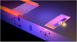
Figure 2. (Right) An artificial atom in the form of a transmon qubit placed on a piezoelectric substrate. (Left) An IDT which can both send and receive acoustic signals to/from the qubit. Image credit: Philip Krantz, Krantz NanoArt.
Download figure:
Standard image High-resolution image
Figure 3. (a) An xmon-style qubit (cross shaped structure on left) is connected through an electronically controlled coupler (center) to an acoustic cavity formed by an interdigitated transducer facing IDT mirrors on either side (right). The qubit structure is fabricated on a separate sapphire substrate from the IDT structure on a LiNbO3 substrate, which is viewed looking through the transparent sapphire substrate. The two are assembled using a flip-chip technique. Similar to a device shown in [35].
Download figure:
Standard image High-resolution imageThere are also very interesting differences between QA and QO. The propagation speed of sound in solids, v, is approximately five orders of magnitude slower than for light in vacuum. This results in short wavelengths for SAWs so that new regimes can be explored that cannot be studied in QO. In one approach, the dipolar approximation breaks down and the superconducting circuit acts as a 'giant' artificial atom. The slow propagation also allows for manipulation of acoustic signals on-chip. This may in the future be used for routing and capture of propagating phonons. Moreover, interesting new functionalities are possible in quantum information due to the intrinsic time delay caused by the slow propagation.
Current and future challenges
Single phonon sources and receivers.
It would be straightforward to make a single phonon source by exciting a qubit and then just waiting for it to emit a single phonon into an acoustic waveguide. There are however two challenges. To prove that this is really a single phonon source is not trivial, one way being to measure its second correlation function; this requires detecting the phonon in some way, possibly by conversion to a photon. Further, one needs to deal with the problem that standard IDTs emit the phonon with equal probability in both directions, using unidirectional IDTs instead.
Giant atoms.
The size of atoms, d, is always small compared to the wavelength of light, λ. This is true for all versions of QO, including cavity- and circuit-QED. In QA, however, the artificial atom made up of a superconducting circuit is normally substantially larger than the wavelength of the acoustic field, i.e. d > λ. This allows us to attach an acoustic antenna on the artificial atom, so that the emission from the atom can be frequency dependent and directional [37]. It has also been shown theoretically that nested pairs of such giant atoms in an acoustic waveguide can be coupled to each other while they are still protected from relaxation into the waveguide [38].
However, artificial atoms can also be giant in another sense, namely if the time it takes the SAW to pass the atom is larger than the relaxation time τ of the atom, d > v τ. This turns out to be a stronger condition than d > λ, so that if the atom is giant in the second sense, it is automatically giant in the first sense. In this case, there is a possibility that a phonon emitted from the atom can be reabsorbed by the atom [39]. This leads to non-exponential relaxation, which was recently demonstrated [40].
Strong coupling to open space.
The acoustic coupling between a superconducting qubit and an open acoustic transmission line can be made quite strong just by increasing the number of finger pairs. Choosing a strong piezoelectric material such as lithium niobate also increases the coupling. This makes it relatively easy to enter the deep ultra-strong coupling regime for acoustically coupled qubits. However, complications can occur if the anharmonicity of the transmon qubit is made much smaller than the coupling, so careful engineering or alternative qubit designs are needed (see below).
Coupling to other quantum systems.
The ability to quantum control phonons in SAW devices poses an interesting possibility, namely the potential for coupling to other quantum systems, such as two-level systems (TLS) or optically-active defect states, such as the nitrogen-vacancy (NV) center in diamond [41] or the divacancy defect in silicon carbide. Some TLS may have strong interactions with phonons through the deformation potential, while perhaps having weaker coupling to electromagnetic fields. SAWs provide the interesting potential to probe such systems and possibly provide an avenue for quantum control [42].
Coupling to nanomechanical devices.
Nanomechanical devices have been extensively developed over the past two decades, in part because of their utility as sensors and in part because they hold potential for quantum memories and for mode conversion, such as between mechanical motion and optical signals. SAWs provide an interesting opportunity for interacting with the mechanical degrees of freedom in these systems, and, with the advent of single-phonon control, the ability to operate and measure such systems in the quantum limit.
Advances in science and technology to meet challenges
Understanding and minimizing losses.
In any kind of quantum information application, losses are unwanted. For a SAW delay line or a SAW coupled qubit, there are several different kinds of losses, including: (i) conversion loss in the IDT; (ii) beam diffraction; (iii) beam steering; and (iv) propagation loss. All of these mechanisms are dependent on a number of parameters, including frequency, temperature, substrate material, sample layout, etc. In order to minimize losses, a systematic study of these loss mechanisms is needed.
Ultrastrong coupling.
With a transmon qubit, it is relatively simple to get very strong coupling to an acoustic transmission line. From the point of view of making a clean study of the ultra-strong and deep ultra-strong regimes, one would like to have an anharmonicity that is larger than the coupling. This is not possible in the transmon qubit, since its anharmonicity is maximum 10% of the qubit frequency [32]. Therefore, it would be interesting to investigate if a capacitively-shunted flux qubit, which can have much higher anharmonicity, can be used.
Unidirectional IDTs.
As mentioned above, a normal IDT structure emits phonons with equal probability in both directions. For certain applications, like a single phonon source, it would be highly advantageous to make qubits and IDTs which are unidirectional. It has been shown that unidirectional IDTs with high conversion efficiency can be made [43], but they have not yet been applied in qubits.
Concluding remarks
SAWs have played an important role in conventional electronics, both for signal manipulation and, for example, as sensors. We believe their role in quantum physics could be equally important, both for fundamental science and for applications in quantum sensing. There are currently several groups with active efforts in this area, with new techniques being developed for coupling and control of SAWs.
Acknowledgments
P D was supported by the Knut and Alice Wallenberg Foundation, by the Swedish research council and by the EU-network SAWTrain. A N C was supported by US Department of Energy through LDRD and FWP funds and by the US National Science Foundation.
2. Quantum acoustics with surface acoustic waves in semiconductors
Martin J A Schuetz1, Johannes Knörzer2, Géza Giedke3,4 and J Ignacio Cirac2
1 Physics Department, Harvard University, Cambridge, MA 02318, United States of America
2 Max-Planck-Institut für Quantenoptik, Hans-Kopfermann-Strasse 1, 85748 Garching, Germany
3 Donostia International Physics Center, Paseo Manuel de Lardizabal 4, E-20018 San Sebastián, Spain
4 Ikerbasque Foundation for Science, Maria Diaz de Haro 3, E-48013 Bilbao, Spain
Status
Surface acoustic waves (SAWs) play an important role in many branches of science and technology. Today, SAW devices are routinely integrated into compact electronic circuits and sensors. This success is due to some exceptional features: (i) SAWs are confined close to the surface, (ii) they can be coherently excited and detected with microwave electronics and (iii) stored in compact high-quality resonators or guided in acoustic waveguides over millimeter distances, and (iv) their properties can be engineered by choice of material and heterostructure [44]. Thanks to these features and further technological progress, SAWs have recently tapped into the emerging field of quantum acoustics (QA), with breakthrough experiments demonstrating the coherent quantum nature of SAWs in the few-phonon regime ([45] and section 1), initiating research on SAW-based quantum devices and technologies. To identify and analyze the challenges and prospects of the field, the analogy with quantum optics (QO) provides useful guidance. Quantum optical concepts and systems suggest novel counterparts in the solid state, with sound (phonons) replacing light (photons) and artificial atoms and quasiparticles taking over the role of natural atoms. As shown in figure 4, this correspondence principle reveals fruitful connections and notable differences between the field of SAW-based QA and some of the most prominent quantum optical systems. As in QO, we can distinguish two main uses of the acoustic field in QA: one, to provide an effective classical field to modify the motional or internal state of a quantum system, while the other is as a quantum system in its own right, using its full state space. In semiconductor implementations, uses of the first type have been demonstrated: single natural and artificial atomic systems have been coherently driven by SAWs with evidence of phonon-dressed atomic states [46] and phonon-assisted dark states (see section 4) being reported, as well as the modulation of energy levels of quantum dots [7]. Moreover, SAWs have been used to provide moving potential wells for semiconductor quasiparticles as a route towards quantum channels for single electrons (see section 3) and the study of many-body quantum ground states of an exciton-polariton condensate in SAW-induced lattices [47].
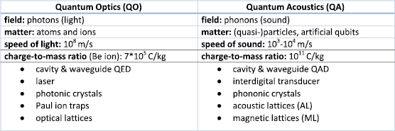
Figure 4. Summary of our correspondence principle between QO and the emergent field of QA. With this dictionary, we can establish insightful connections between these two fields of research, ranging from cavity QED all the way to optical lattices, but also anticipate novel phenomena because we gain access to very different parameter regimes, as exemplified here for the relevant speed of light (sound) and the charge-to-mass ratio. Further details are given in the text.
Download figure:
Standard image High-resolution imageCurrent and future challenges
Experimentally demonstrating hallmarks, such as the Purcell effect, vacuum Rabi oscillations, and superradiance for semiconductor qubits in high-quality acoustic resonators would be the next steps towards cavity quantum acoustodynamics (QAD), as would be the generation of non-classical states of the acoustic modes. Some of these steps have already been realized for superconducting qubits (see section 1). SAWs have been proposed to address a number of challenges faced by implementations of quantum information processing (QIP) in close analogy to QO and here we highlight two representative examples (see figure 5). First, a key ingredient for realizing large-scale quantum networks is the interconnection of independent nodes. Hence, one cornerstone of QIP architectures is a quantum data bus to distribute quantum information. In QA devices, phonons were proposed to serve this purpose on-chip, either by coherently shuttling spin qubits [48] or using resonator or waveguide modes to transport phononic quantum states ([49] and section 5). In particular, SAW modes in piezoactive materials can serve as versatile quantum transducers, even interfacing with vastly different quantum systems in hybrid setups, including superconducting qubits, QDs, color centers and trapped ions [50]. Demonstrating the transfer of quantum information between different qubits using SAWs remains an outstanding challenge. Ultimately, this may pave the way for large-scale on-chip phononic quantum networks ([49] and section 5). To this end, further improvements regarding qubit and SAW coherence, coupling strength and SAW network fabrication are needed. Apart from these technological challenges, interesting theoretical questions arise from the peculiarities of phonon-based architectures in comparison with photon-based technologies. Specifically, the slow speed of sound entails non-Markovian effects in phononic quantum networks, which has intricate implications and will have to be worked out in more detail. Second, a key goal of QIP is to implement large-scale quantum simulators. Promising candidates from QO research are cold atoms confined to optical lattices and trapped ions (see figure 4). In the solid-state setting, SAW-based lattices have been proposed as a scalable platform for quantum simulation, e.g. of long-range Hubbard models [51, 52]. Confining electrons in tunable effective periodic potentials, this would enable analogue quantum simulators reaching parameter regimes very different from their QO counterparts. Their experimental realization, however, poses several demanding requirements, as detailed below.
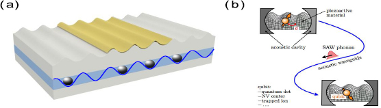
Figure 5. Two representative examples for how QA and SAW research promise new insights in quantum information science: (a) large-scale quantum simulation and (b) large-scale quantum networks. (a) Reprinted figure with permission from [53], Copyright 2018 by the American Physical Society.
Download figure:
Standard image High-resolution imageAdvances in science and technology to meet challenges
The main challenges outlined above require both theoretical and technological advances. First, a thorough development of the quantum theory of sound-matter interactions is needed that can be guided by QO, but must especially take into account the SAW-specific peculiarities such as the low speed of sound, the anisotropic medium in which SAWs propagate and the comparatively large size and intricate structure of artificial atoms, and specifics of quasi-particle dispersion. These can give rise to entirely new phenomena, as has been pinpointed, e.g. in the case of giant atoms, where the dipole approximation breaks down and largely unexplored non-Markovian parameter regimes can be entered (see section 1 and references therein). On the other hand, as SAW-based quantum simulators may provide access to yet unexplored energy scales of long-range Hubbard models, QA extends the scope of testbeds for quantum technologies and QIP, but it also requires the development of advanced methods of quantum many-body theory to guide and interpret these results. The technological challenges concern the fabrication of a compact device comprising all necessary components and its operation in the quantum regime. In the case of large-scale quantum networks, these components include high-quality SAW resonators, low-loss phononic waveguides, and long-lived qubits with excellent coherence properties and good coupling to the phonon modes. Relevant SAW modes have to be singled out and protected from their mechanical environment, as can be achieved by embedding the network in a phononic crystal lattice ([49] and section 5). Ultimately, all these individual building blocks will have to be put together in a single experiment. Regarding SAW-based quantum simulators, the necessary technical requirements for a faithful implementation have been put together in a concise list [52]. As it turns out, all stringent conditions on low temperatures, high SAW frequencies and suitable high-mobility semiconducting materials can be met in state-of-the art experiments, although there is still ample room to explore in order to identify the most promising combination of materials, heterostructures, and quasi-particles. These need to be supplemented with suitable read-out procedures to access the result of the quantum simulation.
Concluding remarks
To conclude, we have discussed and analyzed an emerging research field situated at the intersection between classical (relatively mature) SAW-based devices and quantum science. Using the powerful framework of QO and quantum information science, we have identified several promising research directions which are likely to lead to further rapid progress, both theoretically and experimentally, with both the potential to resolve some of the shortcomings inherent to quantum optical platforms (such as the short-ranged nature of interactions between ultracold atoms in optical lattices or the scalability issues faced by current trapped-ion setups or the large structure size of circuit-QED devices), as well as the ultimate outlook to access yet unexplored parameter regimes. Potential future applications of this still young research field include phonon-based quantum networks, quantum simulation of many-body dynamics, or phonon quantum state engineering, yielding (for example) squeezed states of sound, as required for improved quantum-enhanced sensing and sound-based material analysis.
Acknowledgments
We would like to thank our collaborators with whom we have worked together closely on SAW-related problems: Hans Huebl, Eric Kessler, Mikhail Lukin, Lieven Vandersypen and Mathias Weiler. M J A S would like to thank the Humboldt foundation for financial support.
3. Single electron control by SAWs
Christopher Bäuerle1, Tristan Meunier1 and Christopher J B Ford2
1 Univ. Grenoble Alpes, CNRS, Institut Néel, Grenoble, France
2 Cavendish Laboratory, University of Cambridge, Cambridge, United Kingdom
Status
The control of single electrons is of importance for many applications such as metrology or quantum information processing (QIP) [54]. Originally, the field was motivated by the development of single-electron pumps in the quest for a fundamental standard of electrical current linking the ampere to the elementary charge and the frequency [55]. To have a high-accuracy single-electron pump is of importance as it allows for the precise determination of the value of the elementary charge. This is one of the seven reference constants in the new SI units which will be redefined in 2019 [56]. Single-electron pumps based on surface acoustic waves (SAWs) look promising as the pump can be operated at frequencies of several GHz and hence provide a much larger current compared to other approaches. A quantized acoustoelectric current can be generated when transporting electrons with a SAW through a narrow channel defined by electrostatic gates in a 2D semiconductor heterostructure. The precision of the current plateaus, however, has never exceeded about one part in 104 (100 ppm) due to the relatively shallow confinement potential [55]. In parallel to the development of controlled single-electron transport by SAWs, much research has been devoted to the coherent control and manipulation of a single electron confined in a gate-defined quantum dot, in order to exploit this for QIP [57]. Combining these two approaches has made it possible to transport individual electrons (rather than a stream of single electrons) controllably. A single electron can be transported on-demand by a SAW between distant QDs (see figure 6) with very high fidelity [58, 59]. More recent experiments have also achieved transfer of the spin information of an electron [60] using the same technique and have generated streams of single photons by pumping single electrons into a region of holes [61].

Figure 6. Artist's view of single-electron transport between two distant QDs assisted by a sound wave. The two QDs, defined by the electrostatic gates coloured in violet, are interconnected by a long quantum bus (grey). A single electron, initially trapped in the left QD, is propelled by a sound wave towards the second, distant QD. © Laurent Revellin-Falcoz/CNRS Phototheque.
Download figure:
Standard image High-resolution imageCurrent and future challenges
In quantum technologies, the elementary building block is a TLS—the qubit. Most approaches focus on localised qubits, but some utilise flying qubits, where the qubit is manipulated in flight. Currently, the only technology that uses propagating quantum states is quantum optics (QO), where the quantum information can be coded into photon polarisation. Similar experiments should be possible with single moving electrons in a solid-state device where the Coulomb coupling between electrons provides a means of manipulation. Photons are non-interacting quantum particles and therefore have a longer coherence time than electrons. However, owing to the absence of interactions, it is very hard to construct a two-qubit gate that operates at the single-photon level. An important challenge for electron QO is coherent control of the single electron in flight. This control would allow quantum operations to be performed on the quantum state of the flying electron and hence a solid-state flying-qubit architecture could be implemented.
The question of scalability is a central issue in engineering a spin-based quantum computer [62]. This is likely to require the coherent transfer of a single electron between two distant static qubits, for entangling qubits, error correction, or transfer to and from a quantum memory. Here, SAW-driven QDs have been identified as an interesting platform to control the displacement of the electron spin, with high but precise speed, and low requirements in terms of gate control.
Another application of single-charge and/or spin transfer is the conversion from an electron qubit to a photon qubit, or at least, the read-out of the spin by measurement of the polarisation of the generated photon. These have not yet been achieved, but progress is being made in the generation of single photons by single electrons, a large and essential step in the right direction [61]. Coupled with single-photon detection, perhaps also by SAWs, one can envisage a hybrid solid-state–optical system in which qubits move back and forth between photons and static solid-state dots, allowing the transmission of quantum information over large distances as photons, for quantum cryptography, and the manipulation and entanglement of qubits for use as a quantum repeater to extend the transmission range in cryptography. Here, photon qubits must be captured and stored, and then entangled pairs of photons generated and sent in opposite directions. Deterministic, low-loss and high-fidelity conversion and coupling of qubits are required.
Advances in science and technology to meet challenges
Coherent control of single flying SAW electrons can be realised by bringing two SAW quantum rails into close contact and making them interact by tunnel-coupling [63]. The resulting coherent oscillations of the electron between the two rails would prove the presence of coherent transport. One could also attempt to control the quantum state of the electron on the flight dynamically by ultrafast gate operations. This would allow the observation of such coherent oscillations in the time domain.
To realise coherent single-electron transport is, however, quite challenging. The quantum state of the propagating electron during propagation has to be preserved and should not be perturbed by the environment. Several issues have to be addressed, such as the interactions with the random background of nuclear spins, the fluctuating electrostatic background potential induced by dopants in the semiconductor heterostructures, and the smoothness of the electrostatic gate potential to ensure adiabatic transport. Undoped systems will reduce scattering significantly, but suitable gate designs to make static dots need to be developed.
To build up a scalable flying-qubit architecture also requires the ability to synchronise several single-electron sources. Currently, the limitation lies in the length of the SAW train, which is composed of over a hundred SAW minima. To synchronise two SAW sources, it is hence necessary to know exactly in which minimum the electron is loaded. Using ultrafast gate triggering, it is indeed possible to load a single electron into a predetermined SAW minimum with very high efficiency, but it could be advantageous to engineer SAW transducers that allow generation of a single SAW minimum without sacrificing amplitude. This would allow the suppression of the additional minima, which do not contribute to the single-electron transport, but which represent an additional background perturbation. As far as spin is concerned, minimising the perturbation of the SAW excitation before and after the transfer is key to probing efficient and coherent spin transfer of individual electrons.
Challenges facing the conversion between spin and photon qubits include the efficient emission of single photons (which requires better p -n junction design and the combination of a SAW and a Bragg stack in a pillar projecting higher than the surface on which the SAW propagates). Also, the directions in which spins of the electron and hole with which it recombines are initialised must be orthogonal to avoid decoherence of the emitted photon, requiring particular wafer facets and layers.
Concluding remarks
Although there remain considerable challenges ahead, SAWs have the potential to provide the first electronic flying qubit as well as novel flying-qubit architectures [64]. They are also particularly relevant to plans to use single electron buses for retrieving and distributing quantum information stored in QDs that are embedded in a complex network.
There remain open questions on the operation of these devices as well as their applicability to other materials, such as nuclear-spin-free materials, like 28Si, which looks very promising for spin-based quantum computation, though a piezoelectric layer would need to be added to provide the SAW potential. Further applications and functionalities of these devices are expected in fundamental science, as well as in applied research, including their use as novel phononic lattices [52].
Acknowledgments
We acknowledge funding from European Union's Horizon 2020 research and innovation programme under the Marie Skłodowska-Curie Grant Agreement No. 642688 (SAWtrain), from the French National Agency (ANR) in the framework of its ANR-DFG SingleEIX Project No. ANR-15-CE24-0035 and from the UK EPSRC (Grant No. EP/J003417/1).
4. Coherent coupling between SAWs and defect centers in solids
Hailin Wang
University of Oregon, OR, United States of America
Status
Defect centers in solids can feature exceptional spin properties, including long spin decoherence times and highly efficient optical state-preparation and readout. These spin systems provide a promising experimental platform for quantum computing. High-fidelity quantum control of individual spin qubits has been achieved in a number of solid-state spin systems. An important next step is the control of interactions and the generation of entanglement between individual spin qubits. Coherent interactions between individual defect centers mediated by magnetic dipolar coupling or by long-range optical interactions have been actively pursued. An alternative approach is to exploit spin-mechanical coupling, coupling spins to mechanical vibrations, such as SAWs [50, 41], and to develop a phononic network of defect centers [49, 65]. Mechanical waves cannot propagate in a vacuum. The speed of sound is many orders of magnitude slower than the speed of light. It is thus much easier to confine, guide, and control mechanical waves on a chip than for optical waves.
Coherent interactions between SAWs and defect centers have been demonstrated for single negatively-charged nitrogen vacancy (NV) centers in diamond and for an ensemble of neutral divacancy (VV) centers in silicon carbide. The coherent spin-SAW coupling of a single NV takes advantage of the strong strain coupling of the orbital degrees of freedom of the NV excited states and occurs through the sideband optical transitions, as shown in figure 7(a) [66]. Rabi oscillations of a single NV center have been achieved via the SAW-driven sideband transitions [66]. The coupling between the ground spin states and the SAW can take place via a resonant Raman process, which incorporates a sideband optical transition in a Λ-type three-level system as illustrated in figure 7(b) [67]. These Raman processes allow the use of the strong excited-state strain coupling without populating the excited states, thus avoiding rapid decay of the excited states [67].
Figure 7. (a) Optical sideband transitions of a NV center driven by a SAW at 900 MHz. The red and blue sidebands correspond to the absorption and emission of a phonon, respectively. (b) Schematic of a NV center driven by two optical fields and a SAW via a resonant Raman process that incorporates a sideband optical transition in a Λ-type three level system.
Download figure:
Standard image High-resolution imageFor the coherent spin-SAW coupling of ensemble VV centers in silicon carbide, a SAW resonator that focuses and confines acoustic waves in a Gaussian geometry has been developed [42]. The strong confinement provided by the SAW resonator enables the realization of Rabi oscillations and Autler–Townes splitting, driven directly by the SAWs via the ground-state strain coupling [42].
Current and future challenges
There are two basic challenges for the use of mechanical processes in quantum operations. Coupling of a mechanical system to the surrounding environment leads to mechanical decoherence. Ultrahigh mechanical quality factors are thus needed for the isolation of the mechanical system from the environment. Mechanical systems are inevitably subject to thermal mechanical noises. Although various cooling processes including cryogenic cooling can be used, it is highly desirable if mechanically-mediated quantum operations can be robust against a small number of thermal phonons. In addition, a spin-mechanical system operating in the quantum regime requires the single-phonon spin-mechanical coupling rate to exceed the mechanical as well as spin decoherence rates.
There are also a number of important issues that are unique to phononic quantum networks. The single-phonon coupling rate between a spin qubit and a mechanical mode, which determines the rate of gate operations, scales with  , with m being the mass of the relevant mechanical system. Furthermore, the nearest neighbor coupling of a large number of mechanical resonators leads to spectrally dense mechanical normal modes, which can induce crosstalk between these modes and limits the number of mechanical resonators that can be used in a network. These scaling issues have been well known in well-established phononic quantum systems, such as ion trap quantum computers [68]. Furthermore, high-fidelity quantum-state transfer in a network usually requires a cascaded or unidirectional network. While cascaded optical quantum networks can be realized with chiral optical interactions, as demonstrated with atoms and QDs, chiral acoustic processes and thus cascaded phononic networks are difficult to implement in a solid-state system.
Advances in science and technology to meet challenges
Recent studies in cavity optomechanics have shown that phononic bandgaps can provide a nearly perfect isolation for a mechanical mode from its surrounding mechanical environment [69]. Further advances in phononic engineering can incorporate phononic crystal shields in phononic quantum networks of defect centers. Extensive research efforts on new defect centers, including new materials systems, may lead to the design and realization of defect centers that feature spin properties and spin-mechanical coupling processes that are superior to defect centers, such diamond NV centers, used in current experimental studies. Mechanically mediated quantum operations that disentangle the mechanical subsystem from the rest of the system can in principle be robust against thermal phonons [70]. Further theoretical and experimental explorations of these or related quantum operations in a spin-mechanical system can lead to phononic networks that can operate at elevated temperatures.
The scaling issues discussed above are inherent to any large mechanical system. A conceptually simple solution is to break a large phononic network into small and closed mechanical subsystems. The use of closed mechanical subsystems can not only overcome the scaling problems, but also avoid the technical difficulty of implementing chiral phononic processes [49]. This type of mechanical subsystem can be formed in a network architecture that features alternating phononic waveguides and uses two waveguide modes for communications between neighboring quantum nodes, as illustrated schematically in figure 8(a). A quantum network of spins can be formed when the closed mechanical subsystems are coupled together via the spins, as shown in figure 8(b). This phononic network can also be embedded in a phononic crystal lattice (see figure 8(c)). The successful realization of these complex spin-mechanical systems will depend crucially on the advance in nanofabrication as well as defect center implantation technologies for materials such as diamond or SiC.
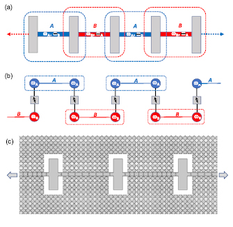
Figure 8. (a) Schematic of a quantum network with alternating waveguides, for which propagation near ωA and ωB is allowed and that near ωB and ωA is forbidden for waveguides A and B, respectively. (b) A phononic network of spins using closed mechanical subsystems. As illustrated by the dashed line boxes, any two neighboring nodes and the waveguide between them can form a closed subsystem. (c) Mechanical design of a phononic network featuring alternating phononic crystal waveguides and a surrounding phononic crystal square lattice.
Download figure:
Standard image High-resolution imageConcluding remarks
With the recent experimental realization of coherent coupling between SAWs and defect centers in solids, one of the next milestones is the use of mechanical vibrations such as SAWs to mediate and control coherent interactions between individual defect centers and corresponding spin qubits. Scaling up these processes in a phononic quantum network can potentially enable a new experimental platform for quantum computing. Advances in phononic engineering, nanofabrication, thermally-robust quantum operations, as well as material sciences of defect centers will be needed in order to overcome the fundamental and technical challenges.
Acknowledgments
This work is supported by AFOSR and by NSF under Grant Nos. 1606227, 1641084, and 1719396.
5. Optomechanics with single quantum dots and elastic waves
Hubert J Krenner1,2, Emeline D S Nysten1, Matthias Weiß1
1 Universität Augsburg, 86159 Augsburg, Germany
2 Nanosystems Initiative Munich (NIM), Munich, Germany
Status
The coupling between elastic waves and single quantum dots (QDs) has a longstanding tradition. In the early days of QD research, their coupling to phonons was considered mainly detrimental. For instance, the predicted phonon bottleneck [71] and phonon induced dephasing [72] were assumed to prevent the realization of QD lasers or limit the fidelity of quantum operations, respectively. As the field developed, many presumed challenges related to the QDs susceptibility to phonons have been found to exist only in very rare settings as it is the case for the phonon bottleneck. Remarkably, concepts have been developed and implemented which deliberately employ the coupling of phonons and for instance excitons in phonon-assisted quantum gates. Dynamic acoustic fields—in the form of a piezoelectric surface acoustic wave (SAW)—were put forward [73] as a high precision tool to regulate the injection of electrons and holes into the dot and thus generate a precisely triggered train of single photons even before the first demonstration of single photon emission by a single QD. Progress in the following years includes the experimental implementation of this acousto-electric scheme [74] and the development of advanced schemes incorporating concepts of solid-state cavity quantum electrodynamics. In parallel, the dynamic modulation of the QD narrow emission lines and the underlying coupling mechanisms were investigated. The observed spectral modulation faithfully reproduces the temporal profile of the phononic waveform [75, 76]. In the case when the frequency of a SAW phonon exceeds the optical linewidth, the system is in the resolved sideband regime [77]. In this key experiment, the QD exciton mediates a parametric coupling between the incoming and the scattered photons with their energies differing by the phonon energy. Figure 9 shows emission spectra of a single QD modulated by a SAW with increasing amplitude.
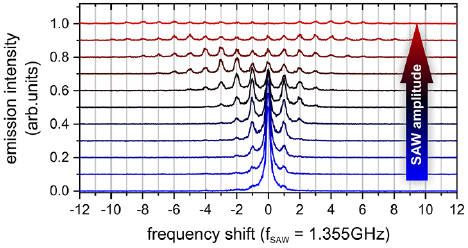
Figure 9. Emission spectra of a single QD dressed with resolved SAW-sidebands. The SAW amplitude increases from bottom to top, resulting in an increase of the number of sidebands.
Download figure:
Standard image High-resolution imageMoreover, the SAW's coherent phonon field was found to modulate the narrow linewidth optical modes of photonic crystal cavities [78] and embedded QDs. This way, the single photon emission can be triggered precisely at the time the emitter is tuned into resonance with the optical mode by the Purcell enhancement. At all other times, the emission is strongly Purcell suppressed [79]. The sound-controlled light–matter interaction in a QD-nanocavity systems can be directly extended to implement entangling quantum gates employing Landau–Zener transition for experimentally demonstrated system parameters [80].
Current and future challenges
Parametric excitation.
The optical two-level system (TLS) of the QD enables parametric mixing of three waves. Already in the first experimental report on SAW-sideband modulation of a QD [77], parametric excitation of the QD exciton was achieved: by optically pumping one of the phononic sidebands interconversion between the optical and mechanical domains was achieved. This scheme enables for instance laser cooling of mechanical motion and for interfacing single semiconductor quantum emitters with propagating or even localized phonon fields. Parametric excitation is needed for future classes of hybrid devices whose operation is governed by classical and ultimately quantum mechanical effects.
Phononic environments.
In general, the coupling of optically active semiconductor quantum emitters to elastic waves is comparably weak. Therefore, a grand challenge lies in the enhancement of the underlying coupling between the elastic field and the quantum emitter, such that the optomechanical coupling exceeds the decoherence rate of the exciton. The governing deformation potential and the strength of the piezoelectric effect are material parameters and thus fixed. Therefore, a strong localization of the elastic field is imperative to enhance the optomechanical coupling. To control these interactions the tailoring of the phononic environment is essential. The coupling between sound and matter can be either enhanced or suppressed in the case of a low or high phononic density of states.
Optical and electrostatic QDs.
The SAW-mediated transport of spins and charges allows for acoustic transfer of quantum information. Such schemes have been conceived and implemented for electrostatic QDs, which have been controlled and interconnected by SAWs [54]. The QDs in focus here are addressed by resonant lasers, enabling spin qubit control [81]. To combine the individual strengths of both QD systems—the long-range SAW-transfer of single charges and spins of electrostatic QDs and the high-fidelity optical programming and manipulation of a chip-based stationary qubit and their mapping onto and entanglement with single photons—would mark another hallmark achievement in the field.
Advances in science and technology to meet challenges
Optomechanical crystals.
These metamaterials supporting both photonic and phononic bandstructures are a native candidate system because they can be combined with QDs. In a recent experiment for instance, the optical and mechanical mode of an optomechanical cavity were coherently controlled by sound [82] (see section 8). Most remarkably, the mean occupation of less than a single coherent GHz phonon can be detected on the incoherent background of more than 2000 thermal phonons at room temperature (RT). When made in the (In)GaAs material system, QDs can be embedded inside the membrane during crystal growth. This tripartite system is illustrated in figure 10. It allows us to confine photons and phonons to smallest volumes and single QDs coupled to these excitations. In addition, waveguide structures (background) route photons and phonons in the plane of the membrane and form an on-chip interconnect. Thus, the fabrication of such devices represents a key enabling technological advancement towards the control of light, sound and matter on a chip.

Figure 10. Optomechanical crystals are a versatile platform to route or confine light and sound of the nanoscale. Embedded QDs can be deliberately coupled to interface the three fundamental excitations in condensed matter, electrons, photons and phonons.
Download figure:
Standard image High-resolution imageHybrid semiconductor-SAW hybrids.
Engineers have been continuously developing SAW and other microacoustic devices over the past few decades, almost exclusively for RF signal processing and communication purposes. Hybrid SAW-semiconductor devices can combine advanced SAW devices fabricated on strong piezoelectrics, such as LiNbO3 and epitaxial semiconductor QDs, harnessing the paradigms of engineering for fundamental studies on QDs [83]. The deliberate hybridization of an epitaxial QD in a membrane and a LiNbO3 SAW-resonator would mark key technological advancements. In such a device, an enhanced optomechanical coupling [8] and a high quality factor phononic mode could be interfaced. In a next, more advanced step, the semiconductor epilayer could be patterned to create a phononic circuitry.
Nanowires.
In contrast to planar architectures considered, heterostructure nanowires are promising inherently 1D platform. Tuning the geometric dimensions of the heterostructure, phononic confinement can be achieved to enhance the coupling between sound and matter. In addition, the NW provides a 1D transport channel to transport charges and spins. Combining the recently demonstrated SAW-regulated tunnel extraction of carriers out [84] and injection into a quantum emitter [85] would mark the achievement of a key scientific and technological challenge.
Concluding remarks
The great strength of acoustic and elastic waves and acoustic phonons in general is that they couple to almost any system either classical or quantum mechanical. Thus, the concepts and challenges discussed above can be applied to other types of quantum systems. Most notably, significant progress has been made on coupling defect centers in diamond and silicon carbide (see section 4) to propagating and localized SAWs [70]. The perspective of optically active QDs integrated in phononic and optomechanical devices uniquely interfaces RF phonons with a highly coherent TLS which can be addressed with near infrared light. They can be even designed for telecom wavelengths, which could ultimately lead to high-fidelity transduction of quantum information from a single GHz phonon to a single optical photon.
Acknowledgments
We thank Achim Wixforth for continuous support and inspiring discussions. This work has received funding by the Deutsche Forschungsgemeinschaft (DFG) via the Emmy Noether Program (KR3790/2-1) and Sonderforschungsbereich SFB 631, and the Cluster of Excellence 'Nanosystems Initiative Munich' (NIM) and from the European Union's Horizon 2020 research and innovation programme under the Marie Sklodowska-Curie Grant Agreement No. 642688 (SAWtrain).
6. Quantum liquids in acoustic potentials
Edgar Cerda-Méndez1 and Paulo V Santos2
1 Universidad Autónoma de San Luis Potosí, San Luis Potosí, Mexico
2 Paul-Drude-Institut für Festkörperelektronik, Berlin, Germany
Status
In a quantum liquid (QL) or superfluid state, an ensemble of integer-spin quasiparticles (bosons) occupy a single quantum state and can flow without dissipation or sustain quantized vortices and persistent currents. At the heart of this state of matter is Bose–Einstein condensation (BEC), a quantum phase transition first predicted by Satyendra Nath Bose and Albert Einstein in 1924–1925. Pure BEC occurs in an ideal non-interacting, bosonic gas at very low temperatures. In contrast, in a QL the interactions are a fundamental feature.
The prospect of a QL in a semiconductor chip is appealing since it allows us to exploit the entanglement of the composing quasiparticles. BEC of excitons (neutral bound states of an electron and a hole) in condensed-matter was first predicted in 1962 [86]. The chase for exciton BEC and QLs became very intense in the last couple of decades, in part due to the availability of fabrication methods for high-quality semiconductor heterostructures, where energy-band engineering enables the quantum confinement of excitons. More recently, composite photon-exciton bosonic quasiparticles (polaritons) have also been intensively studied [87]. Polaritons exist naturally in bulk semiconductors, but in microcavities (MCs), sophisticated heterostructures capable of confining light (see figure 11(a)), it is possible to enhance their population to reach BEC. Polaritons have a micrometers-long de Broglie wavelength  due to their low mass (typically 10−4 to 10−5 the electron mass) and can thus form BECs and QLs even at RT. In GaAs structures, these phases appear only up to a few kelvin, due to the small exciton binding energy.

Figure 11. Polariton microcavity (MC) modulated by SAWs. (a) Scheme of a MC heterostructure. The sequence of gray and blue blocks represent the distributed Bragg reflectors composed of piles of layers with thicknesses of  (
( is the refraction index,
  , and
, and  the light wavelength). The central yellow layer is the
  thick cavity spacer (
 is the cavity refraction index). The QWs are placed at the maximum of intensity of the confined electromagnetic field (red surface) at the center of the spacer. The inset shows calculated depth profiles of the
  and
and  strains of the evanescent SAW field for a SAW with
  . The shaded rectangular area marks the position of the QWs. (b) The interference of two orthogonal SAWs propagating on the MC surface creates a square potential lattice for a polariton condensate excited by a laser beam. The top and lower insets show time-integrated photoluminescence images of a polariton condensate modulated by a SAW of wavelength
  in reciprocal and real space, respectively. Condensation at the corners of the first Brillouin zone (
 ) of the square lattice indicates the formation of a self-localized wave packet called gap-soliton. (b) Reproduced from [25]. © IOP Publishing Ltd and Deutsche Physikalische Gesellschaft. CC BY 3.0.
Download figure:
Standard image High-resolution imageHarnessing the full potential of these QLs in devices is still a big challenge. To achieve this goal, one requires ways to manipulate QLs, such as micro-patterning of the MC or the application of electric, magnetic and/or SAW acoustic potentials. In contrast to static modulation techniques, the amplitude of the potential produced by a SAW can be changed by controlling the amount of power applied to generate them. The spatial modulation of polariton QLs by square lattice potentials created by SAWs has been successfully demonstrated. Interesting phenomena, such as fragmentation of a polariton condensate and gap-soliton formation, have been observed (figure 11(b)) [25].
Current and future challenges
The best studied polariton structures are epitaxially-grown (Al,Ga)As-based MCs [87]. A MC consists of a spacer containing quantum wells (QWs) inserted in-between two distributed Bragg reflectors (DBRs, see figure 11(a)). A non-piezoelectric SAW propagating on the MC surface interacts with polaritons mainly by modulating the exciton levels in the QWs and the MC optical resonance energy with its evanescent hydrostatic strain field. The optimal depth for polariton modulation is roughly  , (
, ( is the SAW wavelength). For example, a typical top DBR is 2 µm thick in an (Al,Ga)As-based MC, so
  8 µm (inset in figure 11(a)) [25]. The value of
  is, thus, coupled to the top DBR thickness.
Reducing  opens interesting perspectives. Polariton-blockade due to polariton–polariton interactions has been predicted for confinement dimensions below
  [88]. The fabrication of arrays of sub-µm micropillars in GaAs MCs by micro-patterning techniques such as reactive ion etching is, however, challenging, due to the thickness of the multilayer MCs (five or more microns). The modulation of MCs by SAWs with
  could allow us to create perfect, amplitude-tunable lattices (see figure 11(b)) with a single polariton per lattice site, where the inter-site tunnelling rate could be controlled. These acoustic lattices are thus solid-state analogues of optical lattices for cold atoms. Additionally, the adiabatic fragmentation on a polariton BEC into single, entangled polaritons (superfluid—Mott insulator transition) by increasing the lattice potential would enable the massive generation of entangled photons [89]. Thus, finding a way of using high frequency SAWs to modulate MC polaritons would be a significant advance. Note that a reduction of
  in the structure of figure 11 also requires a reduction in the thickness of the top DBR, which compromises the MC optical quality. A different approach must thus be used.
Envisaging applications, RT polariton QLs and BECs have been demonstrated in MCs with a polymer, where the exciton binding energy exceeds the thermal energy [87]. Polaritons have also been observed at RT in two-dimensional (2D) materials, such as transition-metal dichalcogenides (TMDCs). TMDCs have interesting spin properties at the M-point valleys of their band structure, which are inherited and enhanced by polaritons [90]. SAW modulation and collective quantum effects in these materials however remain to be studied.
Advances in science and technology to meet challenges
To achieve the ambitious goal of a polariton chip, several challenges must be tackled. For example, in order to be able to modulate polaritons with small  SAWs, novel MC architectures must be designed. One option is to use guided waves propagating along the MC spacer, which would allow the direct acoustic modulation of the QWs with high amplitudes and frequencies. Another option is the open cavity system, where the upper DBR is replaced by an external mirror controlled by piezoelectric positioners [90]. The effects of SAWs in these systems remains to be studied. Finally, an interesting different approach for high frequency modulation (tens of GHz) is laser-generated bulk acoustic waves that travel in the MC [91].
The polariton blockade mechanism also needs to be better understood. There is a considerable spread in the measured values for the polariton–polariton interaction energy (ΔEpp) in polariton ensembles—for single polaritons ΔEpp has only been experimentally accessed very recently [92]. For the polariton blockade, the interaction energy must exceed the natural linewidth of the polariton levels. Here, either very high-quality MCs with long polariton lifetimes must be used or, as recently shown, the interactions must be enhanced, e.g. by using dipolar polaritons [93, 94].
The fabrication of large-size, high-quality TMDC 2D monolayers is readily available, opening the possibility for experiments involving SAW modulation and collective effects. Additionally, the use of van der Waals heterostructures (stacks of different TMDC monolayers) could allow the electrical manipulation of polaritons or dipolaritons in TMDC-based MCs.
Finally, it is unlikely that a potential polariton chip relies on a single modulation technology for manipulation. A mix of complementary static and dynamic techniques would be necessary. The latter requires a strong effort in the engineering of hybrid structures combining SAWs and micropatterning, potentially in combination with in situ electric and/or magnetic fields. Brilliant but isolated efforts have demonstrated the efficient SAW modulation of a QD inserted in a MC in the form of a pillar [95]. The combination of, for example, a condensate in complex 2D potentials with the acoustic modulation by SAWs, opens interesting possibilities for the implementation of enhanced modulation schemes.
Concluding remarks
The modulation of polariton and exciton QLs is an exciting and challenging research field with great applicative potential, many interesting challenges and open questions. SAWs have a special place among the different techniques used, since they allow for a dynamic degree of freedom. Harnessing the full potential of QLs in semiconductor chips to implement advanced devices such as quantum simulators and single photon generators, requires an interdisciplinary effort combining material science, optics, quantum physics and engineering.
Acknowledgments
E C M acknowledges CONACYT and PRODEP project PROMEP/103.5/16/10419 for funding. P V S acknowledges DFG for funding.
7. Interfacing indirect excitons with SAWs
Paulo V Santos
Paul-Drude-Institut für Festkörperelektronik, Leibniz-Institut im Forschungsverbund Berlin e.V., Berlin, Germany
Status
Excitons, electron–hole pairs coupled by the Coulomb interaction, are the main quasi-particles mediating the interaction between light and electronic excitations in semiconductors—exciton-based information storage and manipulation therefore provide a straightforward approach for the processing of optical information in solid-state structures. Two approaches towards this goal based on surface acoustic waves (SAWs) have recently emerged. The first comprises the acoustic modulation of microcavity polaritons—quasi-particles resulting from the strong coupling between excitons and photons in a microcavity. The second, which will be discussed here, relies on indirect (or dipolar) excitons (IXs) in a double quantum well (DQW) separated by a thin tunnelling barrier (see figure 12(a)). An electric field Ez applied across the DQW drives electrons and holes to different wells, while maintaining Coulomb correlations between them. The field-induced spatial separation controls the IX lifetime, which can reach the ms range, thus opening the way for the realization of exciton-based memories and excitonic circuits [96]. The charge separation also imparts an electric dipole moment to IXs, which increases IX–IX interactions [97] and can thus be exploited for IX–IX control gates [98].
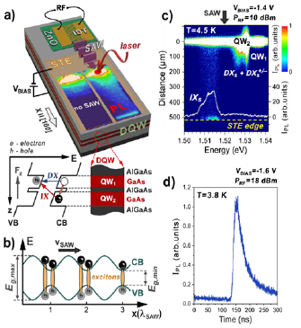
Figure 12. (a) Acoustic transport of indirect excitons (IXs) in a GaAs/(Al,Ga)As double quantum well (DQW) by a surface acoustic wave (SAW) launched by a transducer (IDT) on a piezoelectric ZnO island. The IXs form under a bias voltage VBIAS applied between the semi-transparent top electrode (STE) and the doped substrate. The superimposed PL images compare the emission in the absence and presence of a SAW. Inset: DQW band diagram along the z direction displaying the direct (DX) and indirect (IX) exciton transitions. (b) IX transport by the moving strain modulation of the conduction (CB) and valence band (VB) in a DQW. (c) Spectral PL image and (d) time-resolved PL trace recorded on the transport channel at positions 500 µm and 350 µm away from the exciting laser spot, respectively. Reprinted figure with permission from [101, 102], Copyright 2014 by the American Physical Society.
Download figure:
Standard image High-resolution imageThe transport of charge neutral IXs can be driven by a lateral gradient of Ez. The latter provides an in-plane force that was exploited in functionalities such as IX conveyors [99], and transistors [96]. These field gradients are, however, always accompanied by an in-plane electric field component, which destabilizes excitons. The strain field of a non-piezoelectric SAW (i.e. purely elastic modes devoid of a piezoelectric field) provides, in contrast, a powerful tool for IX control while preserving their stability. Their strain field can induce a type-I periodic modulation of the conduction (CB) and valence band (VB) edges via the deformation potential interaction [100], which captures IXs at the sites of minimum band gap and transports them with the acoustic velocity, vSAW (see figure 12(b)). This strain-induced modulation increases IX stability and contrasts with the type-II modulation by a piezoelectric SAW employed for the transport of uncorrelated electron–hole pairs.
Current and future challenges
A main challenge for the acoustic IX transport is the weak strain-induced amplitude of the band-gap modulation, which in (Al,Ga) structures is typically of a few meV. Efficient long-range IX transport can nevertheless be observed in structures with high IX mobility, as illustrated in figure 12(c). Here, the transport is probed by optically exciting IXs using a focused laser beam and mapping their spatial distribution along the SAW transport path using spatially resolved photoluminescence (PL). The two PL maps superimposed on the device structure of figure 12(a) compare the excitonic PL in the absence (left) and presence (right map) of a SAW. In the former, the PL is restricted to the neighbourhood of the excitation spot. Under a SAW, in contrast, one observes PL at the edge of the semi-transparent electrode (STE) located approximately 500 µm away from the laser spot. The remote PL is attributed to the recombination of IXs transported by the SAW to the edges of the STE [100, 100]. This assignment is confirmed by the spectral dependence of the PL along the SAW channel displayed in figure 12(c). While the spectral signatures of neutral (DX) and charged direct exciton (DX±) around 1.53 eV remain close to the excitation spot, the energy of the weak PL trace along the SAW path and the strong emission at the STE edge correspond to the one for the IXs. The transport dynamics (see figure 12(d)) reveals that most of the IXs remain confined in the SAW potential and move with velocity vSAW. Some of the IXs, however, are delayed due to trapping along the path, which reduces the transport efficiency [102].
Acoustic transistors consisting of gates on the SAW path can store IXs and control their flow [101]. Furthermore, the direction of the IX flow can be bent by 90° by interfering orthogonal SAW beams. The bending relies on the moving square potential lattice created by the interference of the beams, which moves along an oblique direction and transfers IXs between the beams. Lazic et al [101] demonstrates an acoustic IX multiplexer based on this lateral transfer, which enables the coupling of several IX sites and forms the basis for scalable IX circuits.
Advances in science and technology to meet challenges
Prospects for the acoustic IX manipulation includes the storage and transport of single IXs using high-frequency SAWs. It has recently been demonstrated that single IXs can be isolated using µm-sized electrostatic traps [103]—similar potentials can be created by driving IXs along a narrow channel using SAWs with sub-µm wavelengths, as illustrated in figure 13. The discrimination of single IX states relies on the repulsive IX–IX dipolar interactions, which, in a way analogous to Coulomb repulsion, makes the energy of the confined IXs dependent on population (see the inset of figure 13). The quantum state of the transported IXs can be initialized via the absorption of a polarized photon and manipulated along the transport channel by gates or via dipolar interactions with an IX pool close to the channel [98]. Finally, IX can be captured by a two-level trap after transport, leading to the emission of single photons [104]. If combined with the multiplexer concept, the scheme of figure 13 thus forms the basis for a scalable solid-state quantum processor with a built-in interface for long-range information exchange via photons.
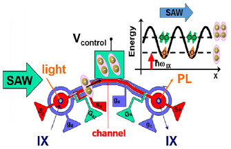
Figure 13. Acoustic transport of single IXs along narrow channels. The IX flow can be controlled by gates along the channel (triangular areas) or by the interaction with an IX reservoir. The inset shows the interaction-induced IX energy levels in the potential of a short-wavelength SAW.
Download figure:
Standard image High-resolution imageAnother important feature of IXs is the combination of a composite boson character with dipolar inter-particle interactions. The latter gives rise to a rich phase diagram for dense IX ensembles including an exciton liquid and a Bose–Einstein-like condensate. The modulation by short wavelength SAWs can be an interesting tool to probe the spatial coherence of these phases.
The application of SAWs for the investigation of both dilute and dense IX phases faces several challenges in fabrication technology, acoustics (e.g. generation of strong SAW beams with sub-µm wavelengths), as well as in material science (IX mobility control, reduction of potential fluctuations) and physics (coherence effects and interaction mechanisms) of excitons. Finally, the small binding energy in GaAs is a major limitation for all IX-based applications. The previously described concepts for acoustically based functionalities can, however, be extended to other material systems with higher binding energies, such as GaN, ZnO heterostructures and IX in 2D-materials [105], where excitons are stable up to much higher temperatures.
Concluding remarks
SAWs enable the creation of a tunable strain field with µm-sized dimensions in semiconductor nanostructures. We have shown here that this field is a powerful tool for the modulation of the energy levels, confinement and transport of IX excitons. Research prospects for the combination of SAWs and IXs include the investigation of dense IX phases as well as the realization of scalable quantum opto-electronic circuits based on the control of single IX entities.
Acknowledgments
We acknowledge financial support from the German Forschungsgemeinschaft, DFG, and the German-Israeli Foundation.
8. Cavity optomechanics with surface acoustic waves
Kartik Srinivasan1,4, Marcelo Wu1,2 and Krishna Coimbatore Balram3
1 National Institute of Standards and Technology, Gaithersburg, MD 20899-6203, United States of America
2 University of Maryland, College Park, MD 20742, United States of America
3 Department of Electrical and Electronic Engineering, University of Bristol, Bristol BS8 1UB, United Kingdom
4 Joint Quantum Institute, NIST/University of Maryland, College Park, MD 20742, United States of America
Status
The growth of the field of cavity optomechanics [106] has been partly brought about by advances in micro and nano-electromechanical systems (MEMS/NEMS) and nanophotonics. These systems, in which optics and mechanics interact via radiation pressure, photothermal, and electrostrictive forces, have been developed across many material platforms and geometries. As the field pushes towards higher mechanical mode frequencies in an effort to achieve stronger interactions and sideband resolution (single-sideband operation), surface acoustic wave (SAW) devices provide a natural platform for exciting high frequency motion and exploring optomechanics with travelling acoustic waves (the regime of stimulated Brillouin scattering) [107].
The rationale for integrating SAW transducers (and more generally, piezoelectric devices) with cavity optomechanics is also driven by other trends. One is the desire to interface RF electromagnetic fields with optics. This has relevance to classical applications, such as microwave photonics, as well as quantum information science, where efficient and low-noise frequency conversion between the microwave and optical domains could remotely connect, via optical links, superconducting quantum circuits. A proof-of-principle demonstration combined capacitive electromechanical transduction with dispersive optomechanical transduction [108], where the latter used a free-space Fabry–Perot cavity modulated by a thin membrane vibrating at MHz frequencies. Realizing a fully chip-integrated transducer will likely require a mechanical frequency in the hundreds of MHz or GHz range, to be sideband-resolved and enable broader conversion bandwidths. At GHz frequencies, capacitive transduction is inefficient, whereas piezoelectric approaches are more naturally suited, as evidenced by the many existing technologies in the GHz domain (e.g. SAW and film bulk acoustic resonator (FBAR) filters).
The integration of such approaches with nanocavity optomechanics has recently been explored. Bochmann et al [109] used integrated electrodes to drive an AlN optomechanical resonator at 4.2 GHz, while Fong et al [110] drove an AlN microdisk resonator at 780 MHz. Balram et al [86] directly integrated SAW technology by using an interdigitated transducer (IDT) to generate 2.4 GHz propagating acoustic waves that resonantly excited a GaAs optomechanical crystal cavity (figure 14). The integration of SAW devices in free-space optical resonators, which can have much narrower linewidths than integrated resonators, has also been considered [111], and SAW-based acousto-optic modulators [112] (see also section 5) have been pushed to >10 GHz operating frequency [113].
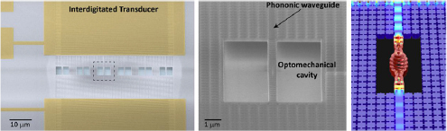
Figure 14. Integration of a SAW transducer with a cavity optomechanical system, as in [86]. An IDT (left) generates a 2.4 GHz SAW that is coupled through a phononic waveguide and resonantly excites an optomechanical cavity (center), whose mechanical breathing mode (right) strongly interacts with a localized optical mode at 1550 nm.
Download figure:
Standard image High-resolution imageCurrent and future challenges
Piezoelectric cavity optomechanical systems [109–113] have illustrated the coherent interplay of the RF, acoustic, and optical fields, and new contexts in which this can be valuable, such as non-reciprocal optical systems, continue to be explored [114]. In general, microwave-to-optical transduction efficiencies have been low (<0.1%) [115], and their improvement is an important challenge, particularly for quantum applications.
A schematic illustrating the microwave-to-optical conversion process is shown in figure 15(a). An RF drive resonantly excites an acoustic excitation, which is then upconverted to the optical domain by a pump whose frequency is detuned from the optical cavity by the mechanical (acoustic) frequency. The optical cavity enhances the coupling between optical and acoustic modes, and its linewidth must be narrow enough so that only the higher frequency anti-Stokes sideband is effectively created. Optical and mechanical quality factors, piezoelectric and optomechanical coupling rates, and coupling of the input RF signal and output optical signal determine the overall efficiency.
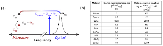
Figure 15. (a) Schematic for microwave-to-optical conversion. ωRF, ωm, ωpump, ωcav are the frequencies of the RF drive/mechanical system/optical pump/optical cavity. (b) Table showing the bulk electromechanical and optomechanical coupling coefficients of some commonly used materials: the electromechanical coupling coefficient ( ) is defined in terms of the piezoelectric coefficient (
 ), the dielectric constant (
 ), and the elastic coefficient (
 ). The optomechanical figure of merit (
 ) is defined (
 ) in terms of the refractive index (
 ), the photoelastic coefficient (
 ), density (
 ) and the speed of sound (
 ). The displayed values are based on the maximum piezoelectric/photoelastic coefficient for the materials.
Download figure:
Standard image High-resolution imageAchieving superlative performance across the optical, mechanical, and electrical domains requires appropriate isolation of the individual sub-systems. High optical quality factor resonators cannot be achieved if the optical field overlaps with the electrodes used in the piezoelectric device. Recent demonstrations of piezo-optomechanical systems [82, 109] have avoided electrode-optical field overlap, and the relative ease with which this is accomplished is a strength of the piezoelectric approach. On the other hand, the extent to which piezoelectric substrates can achieve the ultra-high mechanical quality factors observed in materials like silicon [106] at low temperatures is not yet known.
The choice of material starts with a consideration of its piezoelectric and photoelastic properties, and although the effective coupling strengths can be enhanced by geometry (via strong confinement and high quality factor), the material properties set basic tradeoffs (figure 15(b)). For example, AlN and LiNbO3 have significantly larger piezoelectric coefficients than GaAs. However, GaAs-based devices have exhibited >10 × larger optomechanical coupling rates, due to their larger refractive and photoelastic coefficients [86]. In general, the optomechanical and electromechanical coupling rates should be equal for optimizing conversion efficiency (achieving impedance matching between the RF and optical domains).
Advances in science and technology to meet challenges
As noted above, efficiently mapping the RF input to an acoustic wave that is well-coupled to the optical mode is a major challenge. This can sub-divided into two tasks: converting the RF drive to an acoustic excitation, and coupling that acoustic excitation into a suitable optomechanical cavity. For example, optimizing the approach of [86] might combine more efficient IDTs with acoustic waveguide tapers (or use focusing IDTs), or may require a different type of piezoelectric actuator (e.g. a resonator-based geometry) altogether. Moving from GaAs to a stronger piezoelectric material is another solution. Hybrid platforms that could combine a very efficient piezoelectric material (LiNbO3) with a high-performance optomechanical material (Si) might be the ultimate solution (figure 15(b)), though fabrication and design complexity need to be considered. Alternatively, continued development of materials that show both a strong piezoelectric and photoelastic response, such as BaTiO3, within a thin-film platform suitable for chip-integrated nanophotonics and nanomechanics is another approach [116].
Continued development of nanofabrication processes that limit sources of dissipation (both optical and acoustic) and excess heating, which leads to a non-zero thermal population of the mechanical resonator, ultimately serving as a source of added noise, are also needed. In general, the combination of these different physical domains (RF, acoustic, and optical) in the context of quantum applications is a new field, with many basic experiments (e.g. ultra-low temperature performance of different piezoelectric transducer geometries) still to be performed.
No less important than fabrication and measurement developments is the design of the overall transducer system, which requires both fundamental knowledge and detailed simulation capabilities that address the multiple physical processes involved. Current approaches largely focus on being able to break up the problem into sub-systems that can treated individually, enabling separate optimization steps. Given the recent progress in the RF MEMS community in developing piezoelectric resonators [117], and in the nanophotonics community in achieving record optical performance in piezoelectric platforms [118], the appeal of this approach is quite evident. However, as indicated above, the multiple tradeoffs and considerations involved when integrating the two types of devices suggests that this approach may not yield the best solution, and a more integrated design approach may provide benefits.
Concluding remarks
The integration of SAW devices (and more generally, piezoelectric actuation) with cavity optomechanics enables the coherent interaction of RF electrical waves, acoustic waves, and optical waves in a common platform. This short overview has focused on quantum-limited microwave-to-optical transduction, but the general potential of this platform lies in the possibility of combining desirable characteristics of each of these domains in a way that can be tailored for different applications. However, numerous challenges abound in being able to appropriately combine these sub-systems together while retaining the level of performance available to each in isolation. Continued development of nanophotonics and NEMS, combined with strong interest in the applications of these devices from the quantum information science community, suggests that interest in this topic will continue to increase.
Acknowledgments
We acknowledge the UMD-CNST cooperative research agreement, Award No. 70NANB10H193, the UMD-NIST PREP program, and the ARO/LPS CQTS program.
9. SAWs and 2D materials
Geoff R Nash
Natural Sciences, The University of Exeter, Exeter, United Kingdom
Status
Since the first isolation in 2004 of free standing graphene, an atomically-thin layer of carbon atoms arranged in a honeycomb lattice, there has been rapidly growing interest in not only graphene research, but also in a wide range of other 2D materials [119]. Their large relative surface areas mean that these materials naturally lend themselves to integration with surface acoustic wave (SAW) devices. Not only can the waves and materials couple mechanically, but the electric fields generated by a SAW on a piezoelectric substrate can interact with any charge carriers present. The interactions between SAWs and 2D materials provide both an exciting test-bed to study new phenomena, but could also ultimately form the basis of new electronic and photonic devices.
To date, most research has been focused on the integration of SAWs and graphene, and a comprehensive review of this area can be found in [12]. Theoretical studies predict a range of rich physical phenomena arising from SAW-graphene interactions, such as plasmonic coupling, and graphene's potential as an extraordinarily responsive sensing material is also being exploited for the development of a wide range of SAW sensors. In addition, there has been much recent focus on acoustic charge transport, where the piezoelectric fields associated with a propagating SAW can be used to trap and transport charge, at the speed of sound, over macroscopic distances. Uniquely to graphene, the acoustoelectric current in the same device can be reversed, and switched off, using an applied gate voltage [28]. The use of a lithium niobate thin film, on top of a conducting substrate, allows the same effect also to be observed in more conventional transistor architecture [14], as shown in figure 16. More recently, the piezoelectric coupling of SAWs with charge carriers in other 2D materials has also been explored and SAWs have been used to modulate carriers within molybdenum disulphide [11, 120, 121], as illustrated in figure 17, and black phosphorous [122, 123]. These materials, which have inherent bandgaps, are particularly attractive for optoelectronics and their integration with SAWs has the potential to improve device performance and provide new device functionality.
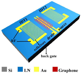
Figure 16. Schematic illustration of the acoustic graphene transistor. Reproduced from [14]. © IOP Publishing Ltd. All rights reserved.
Download figure:
Standard image High-resolution image
Figure 17. Schematic illustration of (a) a MoS2 flake with SAW field under pump pulse excitation, (b) photo-excited. Reproduced from [12]. © IOP Publishing Ltd. All rights reserved.
Download figure:
Standard image High-resolution imageCurrent and future challenges
Materials challenges.
Many of the challenges associated with the integration of 2D-materials and SAW devices are common to the development and exploitation of 2D-materials more generally. For example, many SAW studies have been based on mechanically exfoliated flakes, which tend to be high quality (low numbers of defects) and therefore, for example, have high electron mobility. However, such flakes tend to be only a few tens of micrometers in size, whereas applications require scalable device architectures that are cost effective. Some materials, such as graphene and hexagonal boron nitride (h-BN), can be grown by techniques, such as chemical vapour deposition, and obtained in large areas (on the scale of cm2) commercially. These large areas sheets can then be transferred onto SAW substrates, using relatively well-established processes. In contrast to flakes, however, 2D materials grown this way are polycrystalline, with many of their properties defined by defects associated with the grain boundaries. In addition, the transfer process itself affects the quality of the graphene, introducing wrinkles and tears, and also leads to the device processing being somewhat irreproducible. Direct epitaxial growth of some 2D materials onto SAW substrates, such as quartz and lithium niobite, is possible [120], but receives much less attention compared to growth of these materials on more conventional substrates. A key challenge is therefore how to reproducibly obtain large area, high quality 2D materials on SAW substrate materials, such as quartz and lithium niobate.
Device architectures.
To fully exploit the properties of 2D materials, for example, the ability to modulate the conductivity of graphene using an applied gate voltage will also require the further development of thin film architectures [14] so that conducting substrates can be used as a back gate. The large surface area of 2D materials also often means that the environment can dramatically affect their properties. The significant effect of water on the conductivity of graphene can, for example, be exploited in a SAW humidity sensor, but can also reduce the consistency and reliability of other graphene-based SAW devices. Encapsulation of the active layer will therefore be often required to isolate the 2D materials from the environment.
Advances in science and technology to meet challenges
Materials and architecture.
Advances in materials growth will lead to both improvements in the quality and reproducibility of 2D materials in SAW devices, but will also open up new avenues of research. For example, encapsulation of graphene in hexagonal boron nitride is known to reduce the effect of the environment on the graphene, leading to longer electronic mean-free-paths that are of the same order of SAW wavelengths (a few micrometers). Such large mean-free-paths will allow ballistic effects to be exploited in future SAW devices, and also phenomena that have only been predicted theoretically, for example, SAW mediated optical coupling to plasmons in graphene, to be experimentally demonstrated. The electrically insulating top surface provided by the h-BN also provides a means of incorporating other structures, such as metallic metamaterials to increase the efficiency of optical coupling, into such devices. Heterostructures based on the layering of different 2D materials are also a promising route for the development of photodetectors and light-emitting diodes, and direct growth of these structures will allow further integration of such heterostructures with SAWs [122]. On the other hand, very little work has been carried out investigating how the use of the relatively unusual substrates common in SAW devices might affect the properties of the 2D materials. For example, lithium niobate is highly pyroelectric and changes in device temperature could induce doping in the 2D materials; further study of such effects will be important for the realisation of practical devices.
Future challenges.
Finally, most research to date has focused on the piezoelectric coupling of SAWs with charge carriers in 2D materials. However, the distortions caused by the mechanical coupling of the SAW will also affect the properties of the material. This could be particularly important if 2D materials are combined with emerging phononic structures (for example, see [124]), where SAW displacements can be highly localised, to create novel devices, such as cavity-based sensors, using the 2D material as the sensing element. The potential role of 2D materials in SAW microfluidics, exploiting 2D materials for sensing, filtration or fluid control, is also just beginning to be explored.
Concluding remarks
Work in this area so far has been focused on a relatively small fraction of the huge variety of known 2D materials, which includes the graphene family (e.g. h-BN and silicene), transition metal dichalcogenides, such as molybdenum disulphide, metal carbides, and metal halides. SAWs can be used to probe the properties of these materials, and to provide a test-bed for the exploration of new phenomena. Over the last couple of decades, there has also been considerable interest in the use of SAWs for sensing, quantum information, and in microfluidics. Exciting future research common to all these areas is likely to be the incorporation of 2D materials into resonant elements, whether optical, mechanical, or fluidic (or combinations thereof), and the use of SAWs to probe and control such resonant systems. Such integration could, for example, lead to highly sensitive sensors (section 12), or new devices for quantum technology (see sections 2–8)
Acknowledgments
The author acknowledges the support of his SAW work at Exeter by the Royal Society (No. RG100570), the UK Engineering and Physical Sciences Research Council (Grant Nos. EP/J018651/1 and EP/L015331/1), and the Leverhulme Trust (Research Project Grant No. RPG-2017-60)
10. SAW-driven straintronics
Laura Thevenard, Catherine Gourdon, Pauline Rovillain, Max Marangolo, and Jean-Yves Duquesne
Sorbonne Université, CNRS, Institut des Nanosciences de Paris, 4 place Jussieu 75252 Paris, France
Status
The interaction of acoustic waves and magnetic excitations (spin waves) through magnetoelasticity was proposed in the late 50s, when Kittel showed that their resonant coupling under conditions of equal frequency and wave-vector leads to mixed magnon-phonon modes. The acoustic excitation of GHz ferromagnetic resonance (FMR) modes, or on the contrary, the generation of GHz phonons by spinwaves excited using radio-frequency (RF) magnetic fields was studied in the following decades. The research then mainly focused on nickel and yttrium iron garnets (YIG)—moderately magnetostrictive, but well understood ferro-/ferri-magnets. This coupling was then implemented in the field of electronic device engineering, for instance to turn surface acoustic wave (SAW) delay-lines into magnetically tunable RF components or field sensors [125]. The strong field-induced variations of acoustic wave velocity are indeed particularly well suited to the detection of low amplitude, low frequency magnetic fields, which can be challenging using other magnetometry techniques.
The past ten years have seen a clear revival of the topic with a much stronger focus on potential applications in the field of magnetic data storage, spintronics or magnonics. Information is then encoded by the magnetic state of micro- or nano-structures, the spin-polarization of electrons, or the amplitude/phase of spinwaves. With their low attenuation, their typical frequencies of the order of magnetic precession frequencies, and power-flow confined to the surface, SAWs rapidly emerged as a relevant tool. The effective RF field they induce tickles the magnetization into ferromagnetic resonance. This can in turn lead to the generation of pure electron spin currents in the presence of a heavy-metal top layer [126] (figure 18(a)), or to the full reversal of static magnetization, provided a non-linear coupling regime is reached [127] (figure 18(b)). SAW-driven 'straintronics' [128] have thus joined the likes of spintronics (using current), valleytronics (using valley-dependent properties), caloritronics (using temperature gradients) or multiferroic-based systems (using electrical fields) for non-inductive control of magnetization. Contrary to local electric-field-driven switching however, SAW-driven switching offers the possibility of high efficiency, and remote control of magnetic bits using waveguiding and focusing, or reconfigurable addressing using interference patterns, without the need for local metallic contacts.
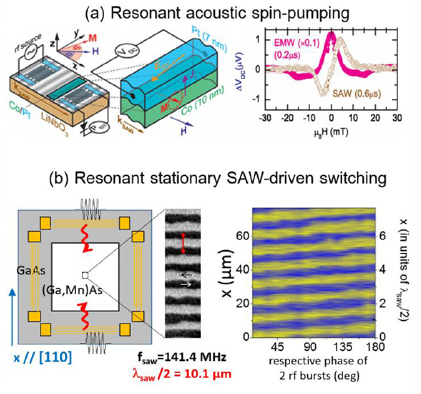
Figure 18. Acoustic-driven magnetization dynamics at resonance. The RF field created by the SAW through magnetoelasticity triggers the magnetization into precessing. (a) Adapted figure with permission from [126], Copyright (2012) by the American Physical Society. When these oscillations are of small amplitude, they generate a transverse spin current detected by the VDC voltage on a Pt strip through the inverse spin Hall effect. (b) Adapted from [127]. © IOP Publishing Ltd. All rights reserved. Two counter-propagating SAWs are sent on a magnetic thin film of (Ga,Mn)As. At the magneto-acoustic resonance, the SAW drives the precessional reversal of magnetization, as evidenced by the magneto-optical contrast. In a stationary geometry, magnetic domains λsaw/2-wide can be created, and positioned precisely by tuning the relative phase of the exciting bursts.
Download figure:
Standard image High-resolution imageCurrent and future challenges
The interaction between SAWs and magnetization is now fairly well understood, but much remains to be done to harness it to actual magnetic architectures. SAWs could, for instance, be the missing ingredient in magnonics, for now limited by the fact that the attenuation distance of spin waves is of the order of a few micrometers for most ferromagnetic materials, limiting prototypes to extremely low damping materials like YIG. Remotely excited SAWs could act as a relay for spinwaves through resonant coupling, and locally modify their amplitude or phase. The optimization of mixed phononic-magnonic crystals, up to now mainly studied numerically [129], could be key for spinwave-based computational circuits.
Concerning the manipulation of static magnetization, localized switching has now been demonstrated using stationary and focused SAWs [127, 130]. Novel architectures which would most benefit from magnetoacoustic coupling now need to be elaborated upon, since current schemes will not be competitive for dense storage devices. The smallest accessible switching size is indeed 'large', i.e. of the order of the SAW wavelength, a few hundreds of nanometers at best. SAW-switching could for instance provide an interesting alternative for remote addressing of moderately dense magnetic bit arrays, provided the transducer design is adapted, using wave-front shaping for example.
The resonant, non-linear behaviour of magnetization dynamics submitted to large amplitude SAWs could also be exploited beyond switching, for instance in magnetic solid-state neuromorphic systems. These require tunable non-linear oscillators which can act as artificial neurons, as recently demonstrated using current-driven spin transfer torque nano-oscillators [131]. SAWs could enable interneuronal synchronization via magnetoacoustic coupling, or even drive the magnetization dynamics, offering the added possibility of a surgical addressing of a given 'neuron' within an assembly.
While most of the above considerations focus on magnetic applications, magnetoacoustics are also highly relevant to the field of phononics. Breaking time-reversal symmetry with magnetism, for instance, leads to non-reciprocal acoustic propagation, with the tantalizing prospect of making phononic diodes. This was studied in the 80s, but could be revisited in thin magnetic films making use of Dzyaloshinski–Moriya interaction [132], or astute patterning to engineer the relevant strain components (figure 19). In graphene-like phononic crystals, magnetism could moreover lead to field-tunable topological protection of SAW propagation: an ultrasonic structure made immune to defects [133]. Elegant demonstrations of this have been shown at low frequencies and large dimensions (Hz/cm) using moving elements, but experiments are still lacking in the realm of the nm/GHz.

Figure 19. Magnetism-induced non-reciprocal SAW propagation. (a) Reprinted figure with permission from [136], Copyright (2017) by the Ameircan Physical Society. The interference of shear and longitudinal magnetoelastic coupling leads to small but finite non-reciprocal SAW velocity variations in Ni/LiNbO3. (b) Reprinted figure with permission from [132], Copyright (2018) by the American Physical Society. A much bigger non-reciprocity may be expected in the presence of Dzyaloshinskii-Moriya interaction (DMI). The magnon-phonon anticrossing then takes place at different SAW wave-vectors, leading to a different acoustic absorption for +ksaw and −ksaw.
Download figure:
Standard image High-resolution imageAdvances in science and technology to meet challenges
SAW-driven magnetization switching has up to now been demonstrated using resonant interaction, at low temperature [127], or fairly inefficient non-resonant coupling in room-temperature ferromagnets [130]. This results from the difficulty of matching SAW frequencies (typically a few GHz) and magnetic ones (often over 10 GHz) at reasonable magnetic fields. Materials presenting both high magnetostriction and low precession frequencies must now be sought after to enable low (or zero) field resonant switching at RT. Moreover, while the industrial sector has optimized very magnetostrictive materials such as Terfenol-D in the bulk form, there is a real need for the synthesis of high quality crystalline magnetostrictive materials in thin-film or multi-layer form. Last but not least, these highly magnetostrictive materials should be grown on efficient piezo-electric films for generation of high SAW amplitude, which demands efforts in synthesis optimization and characterization of these hybrid multiferroic heterostructures.
On the device side of things, magnetoacoustics has so far only exploited a small portion of the elaborate SAW transducer designs optimized by electronic engineers. These can now be implemented in the search of broader bandwidths, more efficient electro-mechanical transduction, but mostly, higher SAW frequencies. This will decrease minimum addressable dimensions and boost the coupling efficiency to magnetization or magnetic defects, making SAWs well suited for sensing NV centers (see section 7) or inducing magnetocaloric effects, as has been shown on MnAs [134].
Finally, the race towards higher frequencies and smaller feature size will entail the need for experimental tools other than optics to study magnetoelastic interaction, be it from the point of view of strain or magnetization dynamics. X-ray diffraction techniques, such as PEEM or XMCD, are viable solutions [135], but they remain cumbersome to implement. Eventually, local electrical probing of the magnetic state by magneto-resistive effects and near-field techniques compatible with SAW excitation should prove to be more adapted to lab-ready approaches.
Concluding remarks
SAWs have proven to be a very useful tool to probe elementary excitations (see sections 1–6 and 8), and magnons are no exception. Far from the academic world, SAWs are commonly used in microelectronic devices, sensors and filters, and are as such a mature technology allowing low power, high efficiency and broad tunability operation. The time is now ripe to harvest the benefits of the fundamental studies of magnetoacoustic interactions of the past decades, and implement these effects into magnetic field-tunable phononic devices, or strain-controlled magnetic structures.
11. SAW devices in future communication systems
Gerhard Fischerauer1 and Werner Ruile2
1 Universität Bayreuth, Bayreuth, Germany
2 RF360 Europe GmbH, Munich, Germany
Status
For about 40 years, surface acoustic wave (SAW) devices have been key components of wireless data transmission systems. They were first applied in high volumes as intermediate-frequency (IF) filters in TV receivers. In comparison with filters based on lumped inductors and capacitors, they were much smaller and required no manual tuning. The same advantages led to their pervasive use in the digital mobile phone systems introduced in the 1990s. One may state that wireless digital communication systems would not have evolved in the way they did without SAW IF filters, RF filters, duplexers, and multiplexers for base stations and mobile phones. Despite the efforts to standardize global communication, several incompatible systems with different frequency bands and different modulation schemes coexist today. The availability of miniaturized frequency-selective components was a prerequisite for the development of multi-band, multi-standard mobile phones as required by the markets. As it turned out, microacoustic devices are the only technology capable of providing this frequency selectivity at low enough cost and with sufficiently small shape factors. As a result, manufacturers today ship billions of units per year.
The technological development has not come to an end yet because the demand for wireless data transmission continues to grow. To accommodate the data traffic associated with human communication, audio and video file distribution, machine-to-machine or vehicle-to-infrastructure communication, and others, regulatory bodies are allocating ever more frequency bands to digital communication systems. Moving from the current fourth generation of digital communication systems (4G, also called LTE (long-term evolution)) to the upcoming fifth generation (5G) will require even more RF filters and multiplexers with even more highly developed characteristics. As in the past (see figure 20 for an example), the challenges will be met by improvements in the filter designs, the material systems, the fabrication methods, and the packaging and integration technologies.
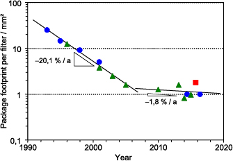
Figure 20. Package footprint of state-of-the-art SAW RF filters (circles [137, 139]), duplexers (triangles [138]), and 1-to-4 multiplexers or quadplexers (square [140]). All areas have been normalized to the number of filter functions in the package. Companies have succeeded in continuously shrinking the footprint between 1990 and 2010. The progress has slowed down since then. It looks as if substantial further size reductions will require technological innovations.
Download figure:
Standard image High-resolution imageCurrent and future challenges
33 frequency bands with center frequencies from 750 MHz to 3.5 GHz have been reserved for 4G networks using frequency division duplexing (different transmit, Tx, and receive, Rx, frequencies). As only a subset of the bands is available in any given region, a world phone must support several bands and standards. This requires two bandpass filters for each link, combined into a duplexer: a Tx filter on the power amplifier output side and an Rx filter on the low-noise amplifier input side (figure 21(a)). A simple dual-band phone requires two duplexers and a switch (figure 21(b)), whereas a modern multi-band phone contains dozens of filters and switches. This explains the pressure on component suppliers to miniaturize their filters and to combine them into modules together with matching-network elements, amplifiers or switches. A modern technique called carrier aggregation (CA), i.e. the simultaneous transmission of data in several frequency bands and over the same antenna to increase the data rate, leads to even more RF filters in the frontend [141]. They must now be combined into 1-to-n multiplexers in packages as small as possible (figure 21(c)). It no longer suffices to design an excellent filter. Instead, it must be an excellent filter in the presence of other filters and the electrical loading, parasitics, and packaging effects this entails.
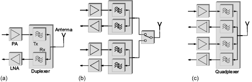
Figure 21. Architecture of a mobile phone frontend. (a) Single-band phone. (b) Dual-band phone. (c) Dual-band phone with CA.
Download figure:
Standard image High-resolution imageSome frequency bands are so close to each other that the filter passband skirts must be very steep to ensure a sufficient stopband attenuation in the adjacent band. They must be even steeper to make up for sample-to-sample variations of the filter center frequency due to fabrication tolerances and for the frequency-shifting effects of influence quantities, such as temperature. In the future as in the past, the required steep passband skirts will only be achievable with filters composed of interconnected high-Q one-port resonators, but the fabrication tolerances and the temperature sensitivity of the devices will have to be reduced.
Further challenges are the reduction of the filter passband ripple (required by higher-order modulation schemes), the reduction of the passband attenuation (to bring losses down to avoid self-heating, to reduce power consumption, to improve signal to noise ratio, etc), the reduction of non-linearities (required because CA causes many mixing products to fall into usable frequency bands), an improved power durability for Tx filters (which would enable further miniaturization), and the production of filters for frequencies above 3 GHz.
Advances in science and technology to meet challenges
Several of the mentioned challenges are linked to the quality factors of the resonators making up a SAW RF filter. Higher Q means smaller insertion attenuation and steeper passband skirts. The Q-factor is determined by the resonator design and the materials used (substrate, metallizations, additional layers). The piezoelectric substrate is also a main contributor to the temperature characteristics of a filter. The two-decade-long dominance of single-crystal LiTaO3 as a substrate material appears to have expired. Its losses, temperature behavior and electroacoustic coupling coefficient k2 all appear insufficient in view of current filter requirements. Instead, filters are built on LiNbO3 with its large k2 and an additional SiO2 overlay with the opposite temperature behavior provides the temperature compensation (temperature-compensated SAW, TCSAW) [142]. New systems with a thin piezoelectric layer over a dielectric substrate such as silicon covered with SiO2 have been developed. Such layered systems have been shown to reduce losses, or increase Q in combination with a very promising temperature stability, paving the way to filter solutions of unprecedented overall performance [143, 144]. More results in this direction are to be expected.
A paradigm shift may lie ahead in the fabrication. In layered structures, the outstanding reproducibility provided by lithography may have to be supplemented by wafer-based processes, such as ion-beam etching, for frequency-trimming purposes, as is already common for bulk-acoustic wave (BAW) filters. Currently, BAW filters are superior to SAW filters at higher frequencies (above, say 2 GHz) in terms of resonator Q. Advanced devices, such as TCSAW and piezo-layer based filters, may tip the scales in favor of SAW filters again. It remains to be seen, however, if SAW filters can really conquer the frequency range above 3 GHz.
Filter suppliers already have the ability to quantitatively describe wave propagation in layered structures, loss reduction by local mass loading, electromagnetic coupling resulting from miniaturization, temperature effects, power durability, and nonlinearities. Further progress in modelling and simulation skills will result in more sophisticated designs, which will be realized by advanced substrates and fabrication processes. This coevolution of modelling, materials and processes will lead to more complex SAW structures with outstanding performance.
Concluding remarks
For four decades, microacoustic devices have played a key role in the development of wireless systems. On the one hand, they have benefited from the phenomenal success of mobile phones and of smartphones. On the other hand, telephone and infrastructure suppliers have benefited from the capabilities of microacoustic devices in that they could utilize the available frequency spectrum in the most efficient way. The current and future complexity of multi-standard phones will most certainly increase the pressure to develop more complex microacoustic systems in addition to the pure BAW and pure SAW filters that have come to dominate the field until now. Whatever the new filters look like, they will have to contribute to an increase in the effective data rate and to a functional densification of digital communication systems.
12. Emerging SAW sensors and functionalized surfaces: a perfect pair of balances
Alexander Reiner1, Ben Paschke1, Dmytro Denysenko1,2, Dirk Volkmer1,2 and Achim Wixforth1,2,3,4
1 Institute of Physics, University of Augsburg, 86159 Augsburg, Germany
2 Augsburg Center for Innovative Technologies (ACIT)
3 Center for NanoScience (CeNS) and Nanosystems Initiative Munich (NIM), Germany
4 Nanosystems Initiative Munich (NIM), Munich, Germany
This paper is dedicated to our dear colleague Dr Dmytro Denysenko, who sadly passed away.
Status
Sensing is one of the most important tasks for the communication between two or more entities. In our technical world, sensing very often means that a system or a machine probes its own state or the conditions of the environment which then is transmitted to another, very often a decision-making system, let it be for the sake of a reaction of a human. Sensors thus play an important role in the function of complex systems and are extremely widespread everywhere. So far, sensors are mostly restricted to measure one or more properties of an environment or a device, but also more recently the status of vital functions of living beings. Wireless transduction of the sensor output together with the endless opportunities for 'artificial intelligence' will open a wide field of applications for sensors of all kind, one specific challenge being autonomous transportation.
Historically, sensors were first used to measure quantities being important in daily life like temperature, pressure and weight. Then, sensors were developed to extend the sensing capabilities of humans. These included light sensitive devices in spectral ranges where we cannot see, very sophisticated hearing devices, tactile sensors and sensors mimicking our taste and smell perception and others. Especially the latter, olfactory sensors have a very important role in the detection of chemicals like poisons, pollutants, chemical and biological warfare agents and explosives, but lately also for breath analysis for health-related issues. Also, sensors are becoming more and more important in automobiles and the communication between the driver and the car as well as for autonomous driving machines, and finally in so-called smart homes and digital industrialization [145]. In any case, a sensor typically consists of an active sensing device and a 'transducer', picking up a sensor response like a change in conductivity, volume, color, etc, and transducing it into a (machine) readable quantity like a voltage or similar. In many cases, SAW sensors [146] play an important role in the field of the above list of sensing devices, as they combine an outstanding sensitivity and the potential for wireless interrogation.
Current and future challenges
A typical SAW sensor layout for the detection of specific gases is shown in figure 22. Here, we depict the combination of a SAW device with three interdigital transducers (IDTs) [147] and a gas sensitive thin film layer. The center IDT generates a bidirectional SAW propagating along the depicted directions. One of the sound paths on the delay lines is covered by a thin film which is very selective in absorbing a special gas. The selectivity in this case is a result of a tunable pore size and chemistry of a highly porous material like a metal organic framework (MOF) [149]. The phase difference between the SAWs is proportional to the mass loading difference of the delay lines [148]. Sophisticated high frequency signal processing techniques can be applied to extremely sensitively measure such phase differences, hence resulting in an extremely sensitive mass detection chip.
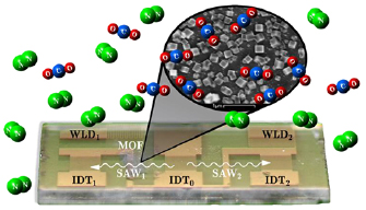
Figure 22. Simple gas sensing SAW sensor consisting of a gas sensitive MOF layer with adjusted pore sizes and a highly sensitive SAW double delay line to convert the mass loading of the chip into a measurable phase difference between the test and the reference SAW. This example is sketched to be able to differentiate between CO2 and N2 molecules in a mixture. Reprinted with permission from [147]. Copyright 2017 American Chemical Society.
Download figure:
Standard image High-resolution imageApart from the development and availability of future 'smart' coating materials, the performance of SAW devices for sensing also crucially depends on many other variables, like the choice of the piezoelectric substrate, attenuating issues in liquids, temperature, frequency, and design fabrication for optimum response. These are important parameters for making SAW a competitive sensor transducer. The advances in modern materials science, both in the physical as well as in chemical and biochemical communities, however, leave a lot of room for confidence for future scientist generations.
Advances in science and technology to meet challenges
All sensors have in common that they are only as good as they are selective and sensitive. It is not very helpful if a gas sensor, say, is more sensitive to temperature changes in the environment than to the presence of the suspicious gas. Also, if one looks, for instance, for NOx detection, the sensor should be very specific and not become easily disturbed or even blinded by the presence of other gases. This is a key challenge which can only be tackled by the design of very specific transducer materials, such as MOFs. The second challenge is the sensitivity. For a SAW device, for example, the sensitivity increases strongly with increasing frequency. Hence, it is very desirable to operate the sensor at frequencies which are as high as possible, which have to be, of course, compatible with the thin film transducing layer on top. Here, highly porous nano systems like zeolithes [150] or, more favorably, the above-mentioned MOF seem to be very promising candidates because of their unprecedented degree of tunability. Not only can the pore size be adjusted over a wide range, they can also be functionalized to become chemically sensitive to adsorbates. Recently, there have even been reports on the electrical switchability of MOFs, thus enabling some kind of built in adaptivity and 'smartness' [151].
Concluding remarks
Our ever-expanding technology-driven world will more and more rely on the interaction between humans and machines. Be it smart homes, smart cars or even the monitoring of our vital parameters and functions. Remote, wireless or even battery-less operation will be of paramount importance. SAW sensors will be the interface between us and the many artificial systems surrounding us in the future. Equipped with and connected to artificial intelligence, machine learning and the internet of things, smart sensors will broaden our own horizon of experience and hopefully lead to a safer environment.
Acknowledgments
This article is based on our longstanding work and experience with SAW devices and sensors in general. It has been funded by numerous agencies like the German Research Foundation DFG and the German Federal Initiative of Excellence. We also gratefully acknowledge endless discussions with many of our colleagues and friends whom we were privileged to work with over the last two decades.
13. Challenges, ideas, and the future of acoustofluidics in closed systems
Henrik Bruus1 and Martin Wiklund2
1 Department of Physics, Technical University of Denmark, Kongens Lyngby, Denmark
2 Department of Applied Physics, Royal Institute of Technology, Stockholm, Sweden
Status
Acoustofluidic technology [152] for handling of particles and fluids on the sub-mm-scale by ultrasound in closed lab-on-a-chip systems has been used for many different purposes, primarily targeting life science-related applications and microfluidics. Recent examples presented at the Acoustofluidics 2018 conference [153], include separation, sorting, washing, mixing, patterning, enrichment, aggregation and 3D culturing of cells. Typical objects being manipulated are biological cells, bacteria, micro/nano-beads, droplets, bubbles, vesicles, or the fluid medium itself. Actuation is mainly performed with bulk-acoustic-wave (BAW) or surface-acoustic-wave (SAW) technology. During the last one to two decades, the field has gradually moved from proof-of-concept demonstrations of unit operations to application-driven device designs and platform developments for specific used-defined needs. Comparing SAW and BAW technology, this transformation of the research field is still young for SAW, partly explained by its greater complexity in terms of the intricate acoustic SAW-fluid interaction and the use of a much wider frequency range. More fundamental work focusing on understanding SAW technology has yet to be done. BAW-based acoustofluidic technology, on the other hand, has recently been commercialized by companies targeting the life science industry, such as AcouSort (Lund, Sweden), FloDesign Sonics (Wilbraham, MA, USA), and Thermo Fisher Scientific (Waltham, MA, USA), the latter company supplying the acoustic focusing cytometer, Attune. Thus, we may expect upcoming SAW-based acoustofluidic applications and products being launched in the future, in addition to early commercialization attempts such as the ArrayBooster and PCR-in-drops platforms by Advalytix (Brunnthal, Germany).
The theory for acoustofluidics is maturing (Bruus [153]), now covering resonances (Baasch [153]), acoustic radiation force on suspended particles (Zhang [153]), acoustic streaming (Bach [153], Qiu [153]), and elastodynamics of the walls (Reichert [153]). Further development of the theory is necessary to fully comprehend the fundamental mechanisms behind acoustofluidics, and to obtain sufficient predictive power to develop design tools for making improved devices. Examples of current improvements in theory include whole-system 3D-modeling (Skov [153]), acoustic tweezers (Thomas [153]), and inhomogeneous fluids (Bruus [153]). However, there is still an unmet demand for improved theoretical understanding of particle-particle interactions at the high particle concentrations often found in biological solutions.
Current and future challenges
For the main application area, acoustofluidics for life sciences, a challenge is to further improve robustness, automation and throughput of devices and methods. Still, manual calibration procedures are often used based on visual inspection through a microscope; see figure 23(a). Integration of acoustic handling systems with detection and readout systems needs to be addressed as well as improving the electrical-acoustical matching, optimizing the energy consumption of the devices and investigating and developing new materials for efficient substrate-fluid coupling and delivery/control of acoustic energy to intended places.
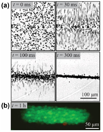
Figure 23. (a) Pictures of 5 µm polyamide beads suspended in water during the first 300 ms of acoustofluidic manipulation in a 2.5 MHz standing wave with 1 MPa pressure amplitude. (b) Picture of calcein-AM-labelled viable A549 lung cancer cells trapped in the pressure node during 1 h of continuous ultrasonic exposure at 1 MPa, 2.5 MHz and 37 °C, the same conditions as in (a). The experiments are adapted from [154].
Download figure:
Standard image High-resolution imageIt is well known that acoustic exposure of ultrasound frequencies to cells and other biological samples may cause various effects [155]. Biological effects of interest, such as viability, proliferation, stress and function of cells, are therefore important to measure. Here, generalized conclusions based on previous studies are risky since ultrasound may cause a variety of physical effects. Different biological samples may also respond differently to a specific set of physical parameters. For example, cells respond differently to standing waves and propagating waves even when frequency, amplitude and energy are the same [155]. Recent studies targeting the cellular state in acoustofluidics have primarily focused on demonstrating the absence of any detrimental effect of significance. However, a future challenge is also to investigate whether acoustic handling may cause beneficial effects on cells or other biological samples. Here, an emerging application field is to use acoustofluidics for tissue modelling and engineering [156]. For this purpose, a recent example of a beneficial effect is the improved quality of cartilage tissue constructs gained by acoustofluidic biomechanical stimulation [156]. For SAW-based acoustofluidic technology, it is also important to extend viability studies to a broader frequency range (in particular to the range 10–1000 MHz), to a broader pressure amplitude range (beyond 1 MPa decoupled from any temperature-related effects [154], see figure 23(b)), and to cells being exposed to more complex acoustic fields that are realizable in SAW devices.
Finally, it is also of interest to apply acoustofluidic technology to other fields than within life sciences. Here, possible areas are, for example, acoustofluidic-based liquid electrolyte recirculation in batteries (Friend [153]), separation of minerals and fossil pollen in geology research, and air-borne filters for nanoparticles and aerosols.
Advances in science and technology to meet challenges
The manipulation of nanoparticles (bacteria, exosomes and viruses) is an important challenge. Progress is reported using electrodes with an angle to the flow direction in SAW devices [157], as well as using the suppression of BAW-induced streaming in inhomogeneous media (Bruus [153]). Furthermore, the first single-cell acoustic tweezing has been obtained by introducing a new transducer design: spiral-formed electrodes on a SAW substrate [158]. Another radically new technique concerns handling of miscible concentration profiles of molecules or nanoparticles as recently proposed in a theoretical study [159], illustrated in figure 24. However, regardless of the specific acoustofluidics setup, good numerical modeling of streaming is needed to meet the scientific and technological challenges involving nanoparticles. A step towards meeting this challenge is the recent theory of pressure acoustics with viscous boundary layers [160], which, compared to a full direct numerical model, reduces the computer memory requirement by a factor of 100 or more using an analytical treatment of the viscous boundary layers. This allows for 3D modeling of streaming in microscale acoustofluidics.
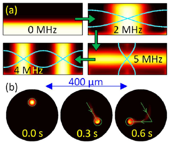
Figure 24. (a) Numerical simulation of rapid (~1 s) acoustic handling of miscible, slowly diffusing concentration profiles of iodixanol shown as color plots from 10 (black) to 30 (white) weight percent. (a) Side view of the sequence of standing BAWs, 0 → 2 → 5 → 4 MHz, each held for 1 s, inside a microchannel with a rectangular vertical cross section. (b) Top view of acoustic tweezing and translation of a local high-concentration region using a SAW-induced acoustic vortex with topological charge 1. Adapted figure with permission from [159], Copyright 2017 by the American Physical Society.
Download figure:
Standard image High-resolution imageCurrently, a limiting factor for fully exploiting the application potential of acoustofluidics is the cost of the glass or silicon components, used because of their high acoustic contrast relative to water. In addition, processing of microstructures within these materials is also costly, time consuming, and sometimes complicated. These limitations are especially severe for applications intended for point-of-care clinical use, where the acoustic separation unit must be a single-use consumable. In a recent theoretical study with experimental support [161], the principle of whole-system ultrasound resonances was introduced to identify and characterize well-suited resonances in all-polymer devices. This principle, combined with off-stoichiometry thiol-ene polymer having tunable acoustic parameters, may point to a way to overcome the challenge of designing and fabricating good, polymer-based acoustofluidic devices.
Concluding remarks
SAW-based acoustofluidics is undergoing a promising scientific and technological development. Given the robust and controllable actuation of the SAW technology in combination with its ability to support complex acoustic fields at a wide frequency range, it is likely that within specific areas it will surpass the less complex BAW technology already used in the first commercial products. Furthermore, SAW-devices for acoustofluidics may be significantly improved in the future by taking whole-system resonances in three dimensions into account in the design process (see [161]). Here, the whole system includes, e.g. the fluid sample, droplet, channel or chamber as well as any supporting solid structure. As a result, we may see handheld or wearable battery-driven devices, and we may find new interesting application areas of acoustofluidics based on SAW technology. To achieve this, efforts within both theory development, numerical modelling, as well as in experimental development need to be accomplished.
14. Acoustofluidics in microfluidics
Julien Reboud1, Jonathan M Cooper1 and YongQing Fu2
1 School of Engineering, University of Glasgow, G12 8LT, Glasgow, United Kingdom
2 Faculty of Engineering of Environment, Northumbria University, NE1 8ST, Newcastle upon Tyne, United Kingdom
Status
The use of surface acoustic waves (SAWs) has become key in the toolbox of different methods available to manipulate fluids, opening up a range of microfluidic applications in medical diagnostics, drug delivery, cell sorting, tissue engineering and life science research. Despite the novelty of many of the methods being proposed, it is perhaps surprising that the first practical demonstration of interaction of SAWs with fluids was made nearly 30 years ago by Shiokawa et al [162], and involved demonstrating the liquid actuation functions of pumping and nebulisation by a Rayleigh wave, on a piezoelectric lithium niobate (LiNbO3) wafer (figure 25(a)). White et al [163], working in the USA, also showed that piezoelectric ZnO thin films on a silicon nitride membrane (or plate) could also be used to create a liquid pump, this time showing the application of Lamb waves to actuate the fluid.
Figure 25. Schematic cross-sectional representation of the different fluidic actuations emerging from interactions between a SAW and a volume of liquid in a droplet (a), leading to deformations on the surface (and ultimately movement, jetting or nebulisation), as well as streaming and recirculatory flows, or within a microchannel (b).
Download figure:
Standard image High-resolution imageMore recently, work by Wixforth's group [164] showed that Rayleigh SAWs can play a particularly powerful role when manipulating very small (nl–µl) microfluidic volumes of liquid—as the majority of the energy associated with the SAW is confined at the piezoelectric surface, and can be efficiently dissipated into the liquid. The smaller the volume, the greater the proportion of its volume that 'feels' this dissipated energy, and thus the more efficient the actuation process (whether this be movement or heating). One further advantage of using SAWs in such systems results from mechanical forces, which cause convective streaming within the liquid, and also, depending upon the nature of the induced flow, may enhance mass transfer for the rapid mixing of reagents [165, 166]. This latter phenomenon saw the first commercial applications of SAWs in life-science instrumentation.
Extensive studies have now also demonstrated that SAW-based acoustofluidics provides the unique ability to manipulate liquids (and particles/cells within them) without contact (offering a contamination-free solution) and in a biocompatible and programmable way [166] (see also section 13). Such capabilities place SAW as a technique of choice to overcome many challenges in fluid handling within microfluidic systems and deliver its long-standing promises. Further advances, which may lead to new applications in wearable diagnostics and ubiquitous sensors and actuators, include decreasing the cost of materials used (e.g. by using thin piezoelectric films on low cost polymer sheets and foils) [167], or increasing functionality (by creating bendable/flexible functions and new flow profiles).
Current and future challenges
For many applications, LiNbO3 has been the piezoelectric material of choice, because it is very consistent in its behaviour and response (e.g. its piezoelectric coefficient is large and predictable for different crystal orientations, despite being relatively expensive, difficult to process and fragile). This has allowed the creation of very complex field structures [168], translating approaches from optical wave shaping (also termed wavefront engineering) into acoustofluidics. To realise new opportunities of SAW-based acoustofluidics, there is a need for new strategies to further integrate the piezoelectric actuator with other sensing and microfluidic functions to enable new low-cost and low power solutions—opening up new challenges in fluid mechanics and acoustics.
Over the last few decades, the liquid has often been processed as a 'wall-less' droplet placed directly onto the piezoelectric surface to maximise the energy transfer (figure 25(a)). The fluid may also be contained within an elastomeric microchannel with a defined geometry (figure 25(b)), with the possibility of allowing the reuse of the actuator [169]. However, the manufacturing and assembly of such devices are complex, limiting their practical applications. As an alternative, SAW manipulations can be produced on a thin disposable chip placed on the surface of the piezoelectric SAW substrate, which can act as a disposable biochip [170]. Such chips have come to be known as superstrates as they sit in contact with the piezoelectric substrate. Their design can be further modified through the introduction of arrays of microstructured features in order to create phononic crystals [171], producing new complex acoustic fields, which can also be used to control liquid flows and interfaces [172]. However, the physics of the complex interactions between the liquids, the newly shaped acoustic field and the different interfaces of the system can be challenging to model, predict and control.
Another integration strategy is to deposit piezoelectric films, such as ZnO and AlN, onto a variety of substrates including silicon, metals, glass and plastics. This will provide new opportunities for integration whilst bringing about a dramatic decrease in material costs, and opening the way for implementing integrated, disposable, or bendable/flexible lab-on-a-chip (LOC) devices [167]. However, there remain issues including their performance and reliability as well as the development of low-cost manufacturing methods.
Advances in science and technology to meet challenges
Acoustic waves generally manifest on timescales of microseconds and produce surface deformations on the piezoelectric wafer that may be below a few tens of nanometers. In contrast, the deformations on fluid surfaces generally respond on the order of milliseconds with displacements that may be a few microns in size. The subsequent flows within the bulk of the liquids provide functionalities in seconds and with distances on the order of the millimetre and beyond. All commonly-used approaches to simulate these phenomena, from finite-element, finite-volume to finite-difference time-domain methods, have imposed constraining boundary conditions to reach practical computational capabilities, that limit precise predictions. To advance the boundaries of our understanding of acoustofluidics beyond currently well-established wave and flow profiles, new analytical and modelling approaches will be required to bridge these spatio-temporal scales. As an example, new approaches that combine analysis in the frequency domain and time-domain [173] may reveal new behaviours, especially where complex rheological and surface properties are available.
In the field of advanced materials, the recent demonstration of deposition of thin piezoelectric films onto a great variety of solid surfaces has opened up new avenues of development to enable us to implement acoustofluidics functionalities into deformable components (figure 26) [167]. These, in turn, could realise wearable lab-on-chips, able to process liquid samples close to or inside the human body. To date, this capability has been hindered by the high energy loss encountered in these flexible, 'soft' systems, limiting the physical reach of the waves to only a few wavelengths. New opportunities in thin plates (below the wavelength) and new modes of propagation and their combinations [174] may provide a promising avenue to overcome this limitation. In particular, controlling different (crystal) structure orientations by controlling deposition parameters [167], or integrating acoustic metamaterials with anomalous material properties, will provide the capability to generate complex wave patterns on a single substrate. This could enable the integration of actuation (e.g. for both medical diagnostics and therapy) and molecular sensing on a single, deformable and disposable substrate (see section 12 for details on SAW sensing capabilities). In this context, novel materials, such as piezoelectric doped graphene may play a future role in such new LOC systems (see also section 9).
Figure 26. Flexible ZnO/PET SAW device in bending (2 micron thick ZnO film deposited onto 120 micron PET foil which also hosts metal IDTs).
Download figure:
Standard image High-resolution imageConcluding remarks
The field of SAW-based acoustofluidics has begun to reach maturity after an initial exponential growth that has spanned the last three decades. The topic is now generating new practical applications in medical diagnostics and drug delivery applications whilst providing biologists with new tools for life-science research based upon cell manipulations and sorting. A new impetus in the fundamental understanding of the physical processes across spatio-temporal ranges that span many orders of magnitude is still required to enable the techniques to be fully realised, enabling translation of capabilities demonstrated in laboratory settings, into real-world settings. This process is likely to require the bridging of different communities and disciplines, a challenge which is not unique to this field, but nevertheless needs to build upon existing knowledge with a shared vocabulary and cross-disciplinary collegiality.
Acknowledgments
J R and Y Q F are grateful for EPSRC support (EP/P018882/1, EP/P018998/1 and EP/N032861/1). J C acknowledges funding from EPSRC (EP/K027611/1) and ERC (Biophononics, 340117). The authors are indebted to discussions with the members from the UK Acoustofluidics Special Interest Group (https://fluids.ac.uk/sig/Acoustofluidics).
15. Cell manipulation employing surface acoustic waves
Manuel S Brugger1, Florian Rehfeldt2 and Christoph Westerhausen1,3,4,5,6
1 Institute of Physics, University of Augsburg, 86159 Augsburg, Germany
2 University of Göttingen, 3rd Institute of Physics—Biophysics, 37077 Göttingen, Germany
3 Center for NanoScience (CeNS), Ludwig-Maximilians-Universität Munich, 80799 Munich, Germany
4 Center for Interdisciplinary Health Research (ZIG), University of Augsburg, 86135 Augsburg, Germany
5 Augsburg Center for Innovative Technologies (ACIT), Augsburg 86159, Germany
6 Nanosystems Initiative Munich (NIM), Munich, Germany
Status
The application of SAWs to the life sciences arose in the early 2000s and is still a rapidly emerging field. Due to the various powerful possibilities demonstrated based on stirring, mixing and pumping very small amounts of fluids acoustically (see sections 13 and 14), and the effect of acoustophoresis, the potential for more complex applications in cell manipulation has become obvious. While the idea of the manipulation of cells with ultrasonic standing waves is much older [175], the transfer from bulk acoustic waves (BAW) with wavelengths on the size of cells has revealed the actual power of the approach. The different fields, as illustrated in figure 27, can be categorized as (i) manipulation of the medium, mainly based on acoustic streaming, (ii) mechanically moving or trapping cells by acoustophoresis and (iii) employing both the mechanical and electrical properties of SAW to stimulate cells. While for the first two fields mainly Rayleigh waves are applied, most commonly generated on LiNbO3 substrates or ZnO films on transparent substrates, the latter field employs shear waves or mixed modes as well. Acoustic streaming so far has been employed to quantify cell adhesion in low volumes, thereby applying a wide range of shear forces simultaneously to single cells or whole cell ensembles [176]. Here, the cell-substrate interface probed is either on the chip itself or positioned opposite to it. Acoustophoresis applications employ pulsed travelling SAWs with high amplitudes for sorting applications in microchannels [177], standing wave fields for alignment and trapping, as well as phase detuning and chirped IDTs to precisely control cell–cell distances [178]. Exemplarily chosen studies elucidate compound transport, co-culture or multi-cell analysis to name just a few areas [179–181]. Moreover, there are some first reports on employing SAWs for cell stimulation, in terms of increased wound healing by migration and proliferation or drug uptake [182, 184]. While for some studies there are clear indications that the accompanying electrical fields are important, others use coupling fluids to influence cells in more-or-less conventional well-plates. Here, the effect might most likely be caused by enhanced effective diffusion constants. All fields are still of the highest interest, aiming on the one hand towards translation into diagnostics, pharmacy and tissue engineering, but also on the other hand towards basic research towards stem cell differentiation.
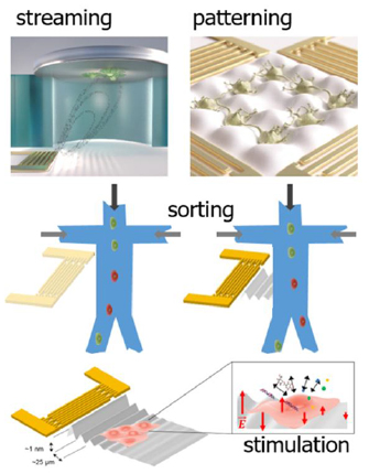
Figure 27. Illustration of categorized fields of applications employing SAWs for cell manipulation: streaming, patterning (© C Hohmann, NIM), sorting and stimulation.
Download figure:
Standard image High-resolution imageCurrent and future challenges
The current and future challenges are of a technological and strategical/translational/transfer-to-market nature. On the one hand, this technology combines RF-technology with microfluidics, cell biology and solid-state physics and is therefore highly interdisciplinary. Here, addressing all the requirements to ensure a controlled environment remains challenging. On the other hand, as with other lab-on-a-chip techniques, the transfer from chip in a lab to real lab-on-a-chip applications is still one of the main challenges; that is, the integration of the peripheral instrumentation, such as pumps, valves and gas-mixers to ensure cell-culture conditions from external, high-end and high functionality instrumentation to a chip, or at least to compact benchtop devices. Such solutions could bring real advantages from physics/engineering labs to life science laboratories or pharmaceutical and clinical applications. As discussed earlier, for such a commercialization and wide usage of the developed SAW-based technologies more than incremental improvements are necessary [183]. To achieve this, high importance clinical/biological tasks without existing simple, easy-to-handle and affordable solutions have to be identified, developed and engineered from the clinical side employing the broad base of possible applications developed so far, instead of arbitrary multiplexing of developed tasks from the engineering side.
Regarding the more technological challenges, longevity and reproducibility of the setups are issues. Here, the combination of reusable setup parts and disposables might help to overcome problems like contamination by debris from cells and tissue. Another challenge is the integration of 3D and mechanically tunable visco-elastic environments going beyond simple coatings [184]. Regarding the relatively new and small field of cell stimulation, the biological response (proliferation, cell stress, calcium release, membrane permeability, organization of the cytoskeleton,...) and interaction mechanisms with the electrical and mechanical fields of SAW have to be studied and understood. A highly interesting field here is elucidating the possible impact of SAW for stem cell differentiation in analogy to mechanically guided differentiation of these cells by Young's modulus E of the substrate [185].
Advances in science and technology to meet challenges
The strategical/translational challenges, especially the inversion of the approach starting from the biological task, require even more interdisciplinary communication to make those communities meet who identify the actual need of solutions and those who have the expertise in acoustic manipulation of micron sized soft matter.
However, on the technological side, to increase the degree of precision and deliberate control of cells hybrid setups may become more important. The use of wave guides, resonator and phononic crystals can help to gain precision, reduce losses and increase the effective amplitudes for even lower input signals. Moreover, towards better 3D control combinations of BAW and SAW could be advantageous and more simple to implement, compared to devices limited to the use of SAW. Towards more in vivo-like environments, hybrids of SAW-chips for cell trapping and stimulation with covalently bound, thin (sub-wavelength) elastic polyacrylamide (PA) gels are promising candidates. By fabrication of very soft gels (e.g. bulk Young's modulus E = 1 kPa) of different thicknesses, the effective Young's modulus Eeff, the cell experiences can be adjusted, as shown in figure 28. Another significant increase of functionality to a level not reached from other cell manipulation techniques is combing the enormous sensing potential of SAW sensors (see section 12) with the one of SAW actuators.
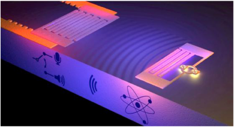
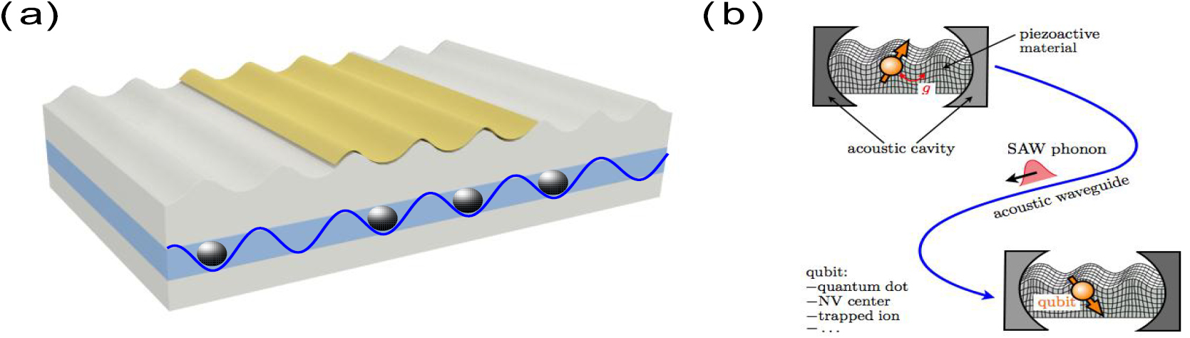
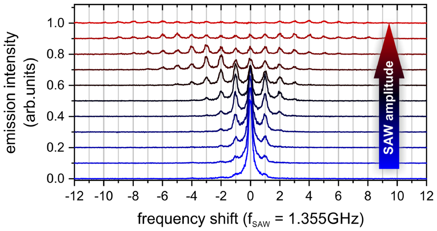
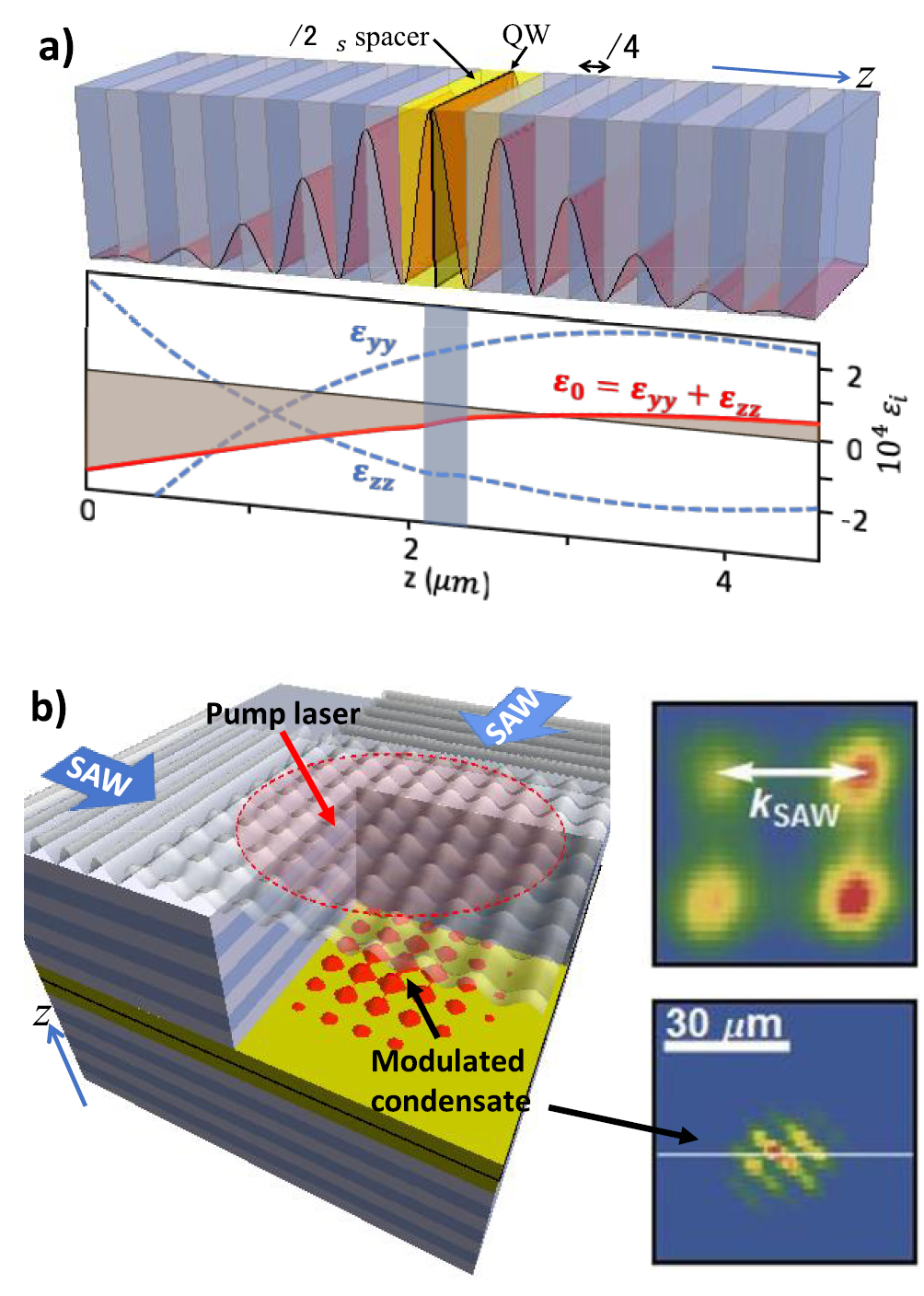
Figure 28. (Top) Live stain of B35 cells on a PA coated SAW chip (thickness = 25 µm, Ebulk = 1 kPa, Eeff ≈ 5 kPa) 7 d after seeding. (Bottom) Effective Young's modulus Eeff of PA gels with Ebulk = 5 kPa as measured by AFM depends on gel thickness on a SAW chip.
Download figure:
Standard image High-resolution image
New promising perspectives in the exploration of neuronal networks have been shown by culturing primary neurons on SAW chips and manipulating the outgrowth of their neurites [186]. Here, the possibilities of using static approaches—e.g. by an appropriate patterning of the chip surface—to produce or manipulate neuronal networks, have proven to be limited. Dynamic approaches like tunable SAW-fields in space and time bear the potential to overcome those. However, significant improvements are still necessary to especially control neuronal networks at will to allow basic biophysics research—such as the correlation between structure, supra-cellular signal propagation and function of neuronal networks. These new and far-reaching perspectives for the long-term need the combination of such novel tools with established ones like multi transistor arrays or other electrophysiological methods.
Concluding remarks
From the three categories of application for SAW-based cell manipulation, especially sophisticated acoustophoresis-based applications, as well as cell stimulation, e.g. for drug uptake, are promising, highly interesting fields of research. The challenges include the need for multiplexing and an inversion of the approach starting from the biological task. Especially, hybrid approaches bundling the expertise of the field of semiconductor devices, material science and cell biology bear the potential to make significant steps and enable new functionalities. In particular, the combination of SAW with visco-elastic environments allows for creation of biomimetic in vivo like environments where active and passive mechanics can be well-controlled to dissect their influence on cellular behaviour (e.g. cardiomyocytes in a beating heart modelled on a chip). Time will tell how fast the progress in this highly exciting research field develops!
Acknowledgments
This work has been sponsored by the cluster of excellence 'Nanosystems Initiative Munich, NIM', BaCaTeC, the Bavaria California Technology Center, the German Research Foundation DFG under the contract 'Erkenntnistransfer projekt—Antibakterielle und Abriebarme Beschichtung von Gleitflächen in Orthopädischen Implantaten' and the 'Center for NanoScience' (CeNS).