
Abstract
We present a study of the electrical, structural and chemical properties of Ti contacts on atomic layer deposited α-Ga2O3 film. Ti forms an ohmic contact with α-Ga2O3. The contact performance is highly dependent on the post-evaporation annealing temperature, where an improved conductivity is obtained when annealing at 450 °C, and a strong degradation when annealing at higher temperatures. Structural and chemical characterisation by transmission electron microscopy techniques reveal that the electrical improvement or degradation of the contact upon annealing can be attributed to oxidation of the Ti metallic layer by the Ga2O3 film in combination with the possibility for Ti diffusion into the Au layer. The results highlight that the grain boundaries and inclusions in the Ga2O3 film provide fast diffusion pathways for this reaction, leaving the α-Ga2O3 crystallites relatively unaffected—this result differs from previous reports conducted on β-Ga2O3. This study underlines the necessity for a phase-specific and growth method-specific study of contacts on Ga2O3 devices.
Export citation and abstract BibTeX RIS

Original content from this work may be used under the terms of the Creative Commons Attribution 4.0 license. Any further distribution of this work must maintain attribution to the author(s) and the title of the work, journal citation and DOI.
1. Introduction
In recent years, Ga2O3 has emerged as one of the most promising wide bandgap semiconductor materials for high-power electronic and ultraviolet optoelectronic applications [1]. This compound exists under several phases, labelled α, β,  , κ, and γ [2, 3]. As the only thermodynamically stable phase, β-Ga2O3 has been the most widely studied. There is however a growing interest in the metastable corundum α-Ga2O3 since; (1) it exhibits the widest bandgap energy among all phases of Ga2O3 [4–6] which makes it the most attractive phase for high-power applications, and (2) is isostructural with several other semiconducting group-III and transition metal sesquioxides (e.g. Al2O3, In2O3, Cr2O3, Ti2O3, Ir2O3) enabling a wide degree of freedom for bandgap and conductivity engineering through alloying [7–10].
Contacts are of paramount importance for the operation of semiconductor devices as they strongly influence the device behaviour and performance. Metallic contacts have attracted attention in β-Ga2O3. In particular, Ti has been reported as one of the few metals to form an ohmic contact with n-doped β-Ga2O3 [1, 11]. The determination of the behaviour of a semiconductor-metal contact is usually primarily determined by the electron affinity of the semiconductor in relation to the metal work-function—according to the Schottky-Mott model. However, this is in practice more complex when it comes to materials like Ga2O3. Indeed Yao et al conducted a comprehensive analysis of contacts between n-doped β-Ga2O3 and nine metals (Ti, In, Ag, Sn, W, Mo, Sc, Zn, Zr), covering a wide range of work-functions and annealing conditions [11]. The study concluded that only Ti and In formed ohmic contacts with n-type β-Ga2O3, but also put spotlight on other factors playing a more critical role in the electrical behaviour of the contact, such as morphology and interfacial reaction. Several other studies have highlighted redox reactions upon annealing at the interface between the oxide film and the metal contact such as Ti [12] or Cr [13].
In comparison, no such study has been performed on α-Ga2O3. Ti has been used as an ohmic contact for α-Ga2O3, largely by analogy with the β phase, but no study of the metal/oxide stability with processing has been conducted. It is however important to conduct a phase-specific investigation of contacts as the band alignment and perhaps more importantly the thermodynamic stability of Ga2O3 are inherently different for the β and α phases. In this study, we investigate the electrical, structural and chemical properties of Ti contacts on α-phase Ga2O3 deposited by plasma-enhanced atomic layer deposition (PEALD).
2. Methods
Approximately 250 nm films of unintentionally n-doped α-Ga2O3 were grown on 1 × 1 cm2
c-plane sapphire substrates by PEALD using an Oxford Instruments OpAL PEALD reactor at a temperature of 250
°C—full description of the growth process can be found in reference [14]. From previous investigations [14, 15], it is known that under these growth conditions, the resulting α-Ga2O3 film is grown epitaxially on the α-Al2O3 substrate with [0001] [0001]
 and [11
 0]
0] [11
[11 0]
0] . The film consists dominantly of α-Ga2O3 columns, with amorphous and -Ga2O3 inclusions located between the columns [15]. The films were unintentionally n-doped, as was observed using X-ray absorption spectroscopy and soft X-ray photoelectron spectroscopy by Swallow et al on comparable α-Ga2O3 films deposited by PEALD [16].
Following cleaning in acetone and isopropyl alcohol, metal contacts were defined using ultraviolet lithography and thermal evaporation. Shipley s1813 positive photoresist was developed with MF-319, an aqueous developer containing dilute tetramethylammonium hydroxide (TMAH), after a short post-exposure treatment with chlorobenzene to produce the undercut profile required for the metal lift-off process. After resist processing, 20 nm Ti and 80 nm Au were evaporated by resistive thermal evaporation from tungsten boats, and the patterns were lifted off in acetone. The contact structure consisted of circular pads 180 µm in diameter and spaced 500 µm apart. The samples were subsequently annealed using rapid thermal annealing for 2 min in N2 at temperatures ranging from 350 °C to 600 °C, while one sample was kept un-annealed.
Atomic force microscopy (AFM) using a Bruker Dimension Icon microscope operating in peak force tapping mode was employed to record the topography of the α-Ga2O3 film before and after annealing.
X-ray diffraction (XRD) using a Philips X'pert MRD diffractometer consisting of a Cu K source, a four-bounce Ge crystal monochromator, and a three-bounce Ge crystal analyser was employed to record the structure of the samples before and after annealing.
Electric and photoelectric characterisation was performed using Keithley 2400 source-meter unit coupled to a Signatone probe station. A Thorlabs SL S204 Deuterium light source coupled to a SolarLS ML44 monochromator was used to illuminate the sample with a monochromatic light.
To observe the atomic and chemical structure of the samples, transmission electron microscopy (TEM) lamellae were prepared by focussed ion beam (FIB) sputtering, and high-angle annular dark-field scanning transmission electron microscopy (HAADF-STEM) imaging and energy-dispersive X-ray spectroscopy (EDX) composition measurements were conducted using an aberration-corrected FEI Titan microscope [17] operated at 200 kV and with ADF detector semi-angle of 69 mrad. EDX compositional maps were obtained using the Cliff-Lorimer factor method [18].
3. Results and discussions
Figure 1 shows the XRD 2θ-ω scan of the as-deposited sample and an AFM image of the α-Ga2O3 surface, together with a schematic of the sample structure. The same analysis was conducted on all the annealed sample structures to check for structural changes in the film upon annealing (supplementary information figure S1 (is available online at stacks.iop.org/JPD/54/384001/mmedia)). The Ga2O3 in all the samples exhibited similar XRD and AFM results, verifying that the 2 min annealing procedure did not have any measurable structural effect on the α-Ga2O3 film.

Figure 1. XRD 2θ-ω scans of the as-deposited sample. In inset, schematic of the contact structure and 1 µm × 1 µm AFM scan of the α-Ga2O3 surface. Collated data for all the samples can be found in supplementary information (figures S1–S2).
Download figure:
Standard image High-resolution imageAll the XRD diffractograms (figures 1 and S1) exhibited a clear 0006 reflection from the α-Al2O3 substrate at 2θ = 41.68°, and a 0006 reflection from the α-Ga2O3 film at 2θ = 40.16°—close to its relaxed value at 40.25° [19]. Upon annealing, the α-Ga2O3 reflection was observed to shift towards its relaxed value, indicating that strain relaxation occurs upon annealing, as was reported by Moloney et al [20]. We explain this strain relaxation to the motion of misfit dislocations which were already present at the substrate/film interface in the samples before annealing [15]. Another peak, at 2θ = 38.20° corresponds to the 111 reflection from the Au contact layer. It can be pointed out that there is no distinguishable signal near 44.4° associated with Au 200 reflection, which indicates that the Au is dominantly (111)-oriented. We also observed that upon annealing, the Au 111 reflection becomes more intense and sharper, suggesting an increase in crystalline quality of the Au layer in the (111)-orientation. This agrees well with previous reports of significant recrystallisation of Au films upon annealing at similar temperatures and timescales [21]. We finally note that no reflection associated with the Ti layer could be observed, which is not unexpected due to the low thickness of the layer and the fact that the most intense reflection of Ti would be expected to occur at the same angle as the intense α-Ga2O3 0006 reflection.
The AFM data (figure 1 inset) displays triangular features that are characteristic of the symmetry of the α-Ga2O3 crystal, and exhibits an RMS roughness of 3.8 nm over a 1 µm × 1 µm scan size. This result remained relatively constant over the sample set, with similar morphologies and RMS roughnesses ranging between 3.8 and 4.5 nm (figure S2)—confirming that the α-Ga2O3 film and surface was not significantly affected by the annealing treatment.
The electrical characteristics of the samples were investigated in order to identify the behaviour of the metal contact with the α-Ga2O3 film. Because the α-Ga2O3 films were highly resistive, as expected from non-intentionally doped material, the characteristics were obtained under 240 nm light illumination. Liu et al showed that photoelectric measurements do not affect the ohmic or rectifying nature of a contact [22]. This is illustrated in figure 2(a) for the as-deposited structure, from which we can conclude that Ti forms an ohmic contact with α-Ga2O3. An ohmic contact was also reported for Ti on β-Ga2O3 [11, 12, 22]. This is generally explained using the Schottky-Mott model, since the work-function for Ti of 4.33 eV and the electron affinity for β-Ga2O3 of 4.00 eV [23] result in a low Schottky barrier height—although other factors have been found to play a role, as acknowledged in the Introduction. In the case of α-Ga2O3, the electron affinity has been predicted at 3.62 eV [24], which implies that a similar ohmic behaviour could be expected.

Figure 2. (a) I–V characteristic of the as-deposited structure under dark and 240 nm illumination conditions. (b) Summary plot showing the photocurrent measured at 10 V of the sample set as a function of the annealing temperature. Collated data for all the samples can be found in supplementary information (figure S3).
Download figure:
Standard image High-resolution imageAll the structures exhibited a similar ohmic behaviour irrespective of the annealing temperature (figure S3). We observed however that the photoconductivity varied greatly with annealing temperature. We illustrate this in figure 2(b) by reporting the photocurrent measured at 10 V. We can see that, following an initial decrease at 350 °C, the photocurrent increased nearly 3-fold upon annealing, resulting in an optimal performance for annealing at 450 °C. The photocurrent rapidly degraded for greater annealing temperatures, where the photocurrent dropped 10-fold for the 600 °C annealed sample compared to the optimal 450 °C annealed sample. A similar dependence with annealing temperature has been reported for n-doped β-Ga2O3 [11] and with variations of the same order of magnitude as what we observed. This dependence was attributed to interfacial reactions at the contact interface. Although we did not observe any morphological or structural change with annealing of the uncontacted material, based on AFM and XRD measurements, it cannot be ruled out that variations of resistivity of the Ga2O2 film itself with annealing could occur and play a role in the observed trend. However, the similarity with previous literature leads us to look closer at changes in the contact structure. To understand the origin of such variation, we conducted TEM observation of the as-deposited sample, of the sample annealed at 600 °C, and finally, of the sample annealed at 450 °C.
Figure 3(a) presents a cross-sectional view of the as-deposited contact structure. As we reported previously [14, 15], the α-Ga2O3 film consists of crystalline columns originating from the interface with the sapphire substrate and which propagate all the way through the film—in line with the triangular features observed by AFM (figure 1 inset). These columns are clearly visible in the HAADF-STEM image in figure 3(a). Previous work also highlighted that the film contained amorphous and -phase inclusions. Such inclusions can be seen in the picture as regions of slightly darker contrast between the crystalline columns, especially visible at the bottom of the film. This picture also indicates that the interface with the Ti contact is rather defective and not clearly defined. We note in places the presence of nanometre size gaps between the α-Ga2O3 and Ti layers—these are mainly located in the region between the tips of the Ga2O3 columns. This is not unexpected given that this contact was not annealed.
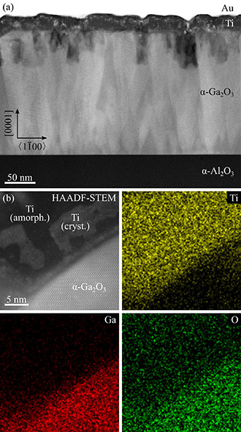
Figure 3. (a) HAADF-STEM image of the as-deposited structure. (b) HAADF-STEM image and corresponding EDX compositional maps of the metal-film region. The images were taken along the  zone-axis.
Download figure:
Standard image High-resolution imageFigure 3(a) also shows strong variations of contrast within the Ti layer, which reflect variations in crystallinity of the material. As seen in the enlarged HAADF-STEM image (figure 3(b)), the Ti layer is largely amorphous (darker contrast regions), with occasional nanoscale regions of brighter contrast which are crystalline. Turning now our attention to the semiconductor/metal interface, the EDX maps (figure 3(b)) show two chemically distinct regions, corresponding to the α-Ga2O3 film and the Ti layer. Some residual amount of O was detected in the Ti layer, which is expected from the sample preparation of Ti-containing foils using conventional (i.e. non-cryogenic) FIB as Ti is a strong getter of species like O or H [25].
Figure 4(a) presents a cross-sectional image of the structure after annealing at 600 °C which, as discussed earlier, exhibited significantly poorer electrical properties. The HAADF-STEM image in figure 4(a) displays a range of significant differences compared to the as-deposited sample (figure 3(a)).
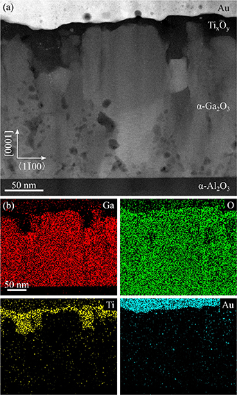
Figure 4. (a) HAADF-STEM image and (b) corresponding EDX compositional maps of the structure annealed at 600
°C. The images were taken along the  zone-axis.
Download figure:
Standard image High-resolution imageFirstly, in the α-Ga2O3 layer we note the presence of dark spots throughout the film, and which were not present in the as-deposited layer. Given that EDX maps did not detect any elements other than Ga and O at these positions, we can then conclude that these correspond to holes within the film. We note that these holes have formed on either sides of the α-Ga2O3 crystalline columns. It is therefore safe to assume that these holes have formed in the disordered part of the film, that is, the inclusions and grain boundaries. We could also occasionally observe O-poor and Ga-rich crystalline inclusions near the top of the film (such as the rectangular-shaped grain in the right-hand side of figure 4)—these were however not a feature commonly found in this sample.
Turning now our attention to the Au layer, we can observe horizontal lattice fringes throughout the film (distinguishable in the left part of figure 4(a), and in figure 5) indicating that the Au layer has further crystallised upon annealing—in agreement with reference [21]. The fringes spacing was measured at 2.35Å, in excellent agreement with the (111) interplanar spacing of Au, which comforts the (111)-orientation noted from XRD measurements. We also observed that the top surface of the Au film exhibited 100s nm bumps (not shown here) which were not present in the as-deposited samples, indicating that significant amount of diffusion occurred during the 2 min anneal.

Figure 5. HAADF-STEM image of the contact region in the sample annealed at 600
°C. In insets, FFT of the α-Ga2O3 and Tix
Oy
regions. The image was taken along the  zone-axis.
Download figure:
Standard image High-resolution imageLastly, we turn our attention to what used to be a uniformly 20 nm-thick Ti layer. The most notable observation is that O is now detected all across that layer (figure 4(b)), showing that the Ti layer in its entirety has oxidised into a Tix Oy layer. Oxidation of the Ti layer has also been reported in β-Ga2O3 [11, 12] (annealed at 400 °C–470 °C); however we note differences in our samples which we describe further in later paragraphs. The Tix Oy layer is now found to conform better to the Ga2O3 film, by occupying the gaps between the tips of the Ga2O3 columns (in the as-deposited film, these regions contained gaps). We note however that the layer thickness varies significantly across the sample, and it appears in places that the Ga2O3 film is directly in contact with the Au layer. Small particles of Tix Oy are also observed at the bottom of the Au layer. This is again indicative of substantial Ti and Au interdiffusion during the anneal process, as was reported by Lee and Peterson [12]. We note, however, that the Tix Oy and Au layers are distinct (with the exception of the small particles), which contrasts strongly with the structure annealed at 450 °C and with previous reports [11, 12], as we will see later.
The oxidation of Ti upon annealing raises the question of the origin of the O atoms. Given that the Ti layer is capped with a thick Au layer, it can be concluded that O comes from the reduction of the Ga2O3 film. If the film were β-Ga2O3, this observation could be explained from a thermodynamic point of view as the Gibbs free energy for the reaction between Ti and β-Ga2O3 is negative for most of the possible oxide forms of Ti, implying there is a driving force for β-Ga2O3 reduction and Ti oxidation. The reduction of β-Ga2O3 by less thermodynamically stable metal contacts has been reported previously [11–13]. In our case, we show that the same result is obtained with the metastable phase α-Ga2O3. However our TEM observations allow us to deduce that the O does not appear to originate from the α-Ga2O3 material itself, but rather from the disordered material (inclusions, grain boundaries) as this would explain the presence of voids between the α-Ga2O3 columns. This makes sense given that disorder, as well as defects in the crystal, are known for acting as fast diffusion pathways in metallurgy—and to dominate the diffusion process at low temperatures.
We would like to point out here a major difference between our results on α-Ga2O3 (annealed at 600 °C) and previous observations made on β-Ga2O3 (when annealed at 400 °C–470 °C). Lee and Peterson reported that the reduction of the β-Ga2O3 film resulted in a defective β-Ga2O3 layer (evidenced by lattice distortions in the TEM images, and presence of Ti) between the high crystalline quality β-Ga2O3 film and the Tix Oy contact [12]. In our study, the defective material corresponds to the disordered and void-containing material between columns, while the majority of the Tix Oy layer is in contact with high quality α-Ga2O3 columns, as illustrated in figure 5. Our data show no sign of Ti and Ga interdiffusion nor lattice distortion in the α-Ga2O3 adjacent to the Tix Oy layer.
We finally note that the Tix Oy layer seems to be largely crystalline albeit defective—as evidenced by the lattice fringes and fast Fourier transforms (FFT) in figure 5. However, we cannot ascertain the exact crystallographic nature of the Tix Oy polymorph. This is perhaps not surprising given that a 2 min anneal duration would be insufficient for the reaction to reach thermodynamic equilibrium. Hence the Tix Oy layer is very certainly highly defective, non-stoichiometric, and may also contain several polymorphs.
We now look at the structure exhibiting the best electrical properties, that is, the structure annealed at 450 °C. As illustrated in figure 6, this sample presents commonalities with the structure annealed at 600 °C, but also presents features of its own.

Figure 6. (a) HAADF-STEM image and (b) corresponding EDX compositional maps of the structure annealed at 450
°C. The images were taken along the  zone-axis.
Download figure:
Standard image High-resolution image
We first notice the presence of dark spots surrounding the α-Ga2O3 crystalline columns, denoting the holes in the disordered part of the film. We observe however that these holes are significantly smaller than the ones we observed above, in the structure annealed at 600 °C. Following the previous conclusions, this is indicative of Ga2O3 reduction by Ti—oxidation of Ti by β-Ga2O3 is thermodynamically expected at this temperature and has been reported previously [11, 12]. This is confirmed with the EDX maps (figure 6(b)) which show that O is detected in the Ti layer. The smaller size of the holes, in comparison to when annealed at 600 °C indicate that the reaction did not proceed to as much an extent as when annealed at 600 °C. This could be due to the reaction not reaching completion at this temperature, or (aligned with the findings in the following paragraphs) that fewer Ti atoms were available for oxidation.
Another similar feature with the structure annealed at 600 °C is the fact that the Tix Oy layer conforms better with the Ga2O3 film, and the presence of Tix Oy nanoparticles at the bottom of the Au layer—although these are also smaller.
A major difference from the data presented in figure 4 is that Ti and Au have more extensively interdiffused when annealed at 450 °C in comparison to when annealed at 600 °C. In figure 6(b) we can observe that Ti is present throughout the bottom half of the Au layer. From the HAADF-STEM image we can see that the Ti-containing Au layer is more granular than the upper Au layer. This resonates with the findings from Tisone et al that extensive diffusion of Ti into Au occurs through grain boundaries at such temperatures [21]. In comparison, we find only minute amounts of Ti in the more bulk-like upper part of the Au layer. Lastly we observe that a thin Tix Oy interlayer has formed underneath the top surface of the Au contact. This finding is reminiscent of Ti accumulation and oxidation at the free surface of Au that was observed for contacts on Si and GaAs [26, 27].
Although the Ga and Ti EDX maps appear to form distinct regions, the top 5–10 nm of the Ga2O3 film seems to contain Ti. This is not unexpected, as this was reported for Ti contact to β-Ga2O3 annealed at the same temperature [11, 12]. Moreover, Ga2O3 and Ti2O3 can both exist under the corundum α phase, making interdiffusion more probable—Barthel et al reported the growth of α-(Tix Ga1 - x )2O3 alloys with contents up to x ∼ 5% [9]. This observation should however be nuanced as projection effects at the rough Ga2O3/Tix Oy interface may play a role.
It is interesting to observe that the Ti layer has spread significantly through the contact structure upon annealing at 450 °C, while it is largely confined to its initial position upon annealing at 600 °C. Based on our observations, we identify three main interconnected and competing processes that could determine the extent of Ti atomic migration during the annealing process. These are (1) Ti diffusion at Au grain boundaries, (2) Ti oxidation by Ga2O3, and (3) Au recrystallisation. For example, when annealed at 600 °C, the Ti atomic migration through the Au contact may have been impeded because the Ti layer became oxidised more rapidly, and/or because faster Au recrystallisation reduced the amount of grain boundaries that could act as fast Ti outdiffusion pathways, thus contributing to the encapsulation of the Tix Oy layer.
The data presented here provide evidence that several atomic migration processes are at play when annealing Ti/Au contacts on α-Ga2O3 and affect the contact performance. The increased electrical properties of the structures annealed at temperatures ∼450
°C have been attributed to the formation of a thin Tix
Oy
layer and to the diffusion of Ti into Au to form a low resistivity layer [11, 12]. Apart from observing that Ti oxidation occurs through the disordered regions of the α-Ga2O3 film, our observations align well with these reports. The poorer electrical properties of the samples annealed at temperatures  450
°C can be attributed to the formation of a thicker and defective Tix
Oy
interlayer through most extensive reduction of the disordered regions of the Ga2O3 film. This Tix
Oy
interlayer exhibits varying thickness between the α-Ga2O3 crystal and the Au metal contact (so that in places the two are in direct contact), but is generally thicker than when annealed at 450
°C owing to Ti diffusion into Au being hindered. This thicker, defective, non-uniform Tix
Oy
layer will have limiting effects on the conductivity and current density at the contact, thus deteriorating the contact performance and affecting the reliability and predictability in a device context.
450
°C can be attributed to the formation of a thicker and defective Tix
Oy
interlayer through most extensive reduction of the disordered regions of the Ga2O3 film. This Tix
Oy
interlayer exhibits varying thickness between the α-Ga2O3 crystal and the Au metal contact (so that in places the two are in direct contact), but is generally thicker than when annealed at 450
°C owing to Ti diffusion into Au being hindered. This thicker, defective, non-uniform Tix
Oy
layer will have limiting effects on the conductivity and current density at the contact, thus deteriorating the contact performance and affecting the reliability and predictability in a device context.
On a positive note, the oxidation of Ti by the disordered parts of the Ga2O3 film, resulting in a crystalline Tix Oy layer in contact with high quality α-Ga2O3 could open interesting routes for fabricating Tix Oy /Ga2O3 heterostructures—provided improvement and control of the Tix Oy crystallinity can be achieved.
4. Conclusions
We have conducted a structural, chemical and electrical investigation of Ti contacts on PEALD-grown α-Ga2O3 as a function of annealing temperature. We highlight that Ti forms an ohmic contact with α-Ga2O3 irrespective of the annealing temperature. The electrical properties of the contact were found to be optimal for annealing at a temperature of 450 °C. We attribute this to the formation of a thin Tix Oy layer (obtained through Ga2O3 reduction by the Ti contact) in contact with a Ti-containing Au layer (obtained through Ti diffusion into the Au contact). We found that the electrical properties degrade rapidly for anneals conducted at greater temperatures. We identify that this relates to the more extensive interfacial reaction between the Ti and Ga2O3 films, and to the restricted diffusion of Ti into Au. Although this result presents similarities with that obtained on β-phase materials, we underline the morphology of the semiconductor/contact interface is dependent on the phase and growth method. Here we observed that the Ga2O3 reduction occurs from the inclusions and grain boundaries between the α-Ga2O3 columns that provide a fast pathway for diffusion.
Data availability statement
The data that support the findings of this study are openly available at the following URL/DOI: https://doi.org/10.15129/2c4c3e3a-71e4-4646-bfaa-d4ec62941c44.
Acknowledgments
The authors acknowledge support from the Royal Society (RGS\R1\201236), the Engineering and Physical Sciences Research Council (EP/T517938/1; EP/P00945X/1; EP/M010589/1; EP/K014471/1), and the European Union's Horizon 2020 research and innovation programme (Grant Agreement No. 823717-ESTEEM3).